Imaging coherent transport in graphene (Part II): Probing weak localization
Abstract
Graphene has opened new avenues of research in quantum transport, with potential applications for coherent electronics. Coherent transport depends sensitively on scattering from microscopic disorder present in graphene samples: electron waves traveling along different paths interfere, changing the total conductance. Weak localization is produced by the coherent backscattering of waves, while universal conductance fluctuations are created by summing over all paths. In this work, we obtain conductance images of weak localization with a liquid-He-cooled scanning probe microscope, by using the tip to create a movable scatterer in a graphene device. This technique allows us to investigate coherent transport with a probe of size comparable to the electron wavelength. Images of magnetoconductance vs. tip position map the effects of disorder by moving a single scatterer, revealing how electron interference is modified by the tip perturbation. The weak localization dip in conductivity at is obtained by averaging magnetoconductance traces at different positions of the tip-created scatterer. The width of the dip yields an estimate of the electron coherence length at fixed charge density. This “scanning scatterer” method provides a new way of investigating coherent transport in graphene by directly perturbing the disorder configuration that creates these interferometric effects.
1 Introduction
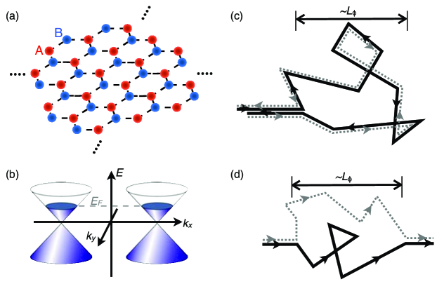
Graphene, a single atomic layer of carbon atoms in a hexagonal lattice (figure 1a), shows quantum phenomena [1] from the coherent flow of electron waves. These include the quantum Hall effect [2], the Josephson effect [3] and weak localization [4]. Graphene has an unusual band structure created by the interaction of electrons on the two sublattices, labeled A and B in (figure 1a): the conduction and valence bands are conical, and they meet at a point in -space, the Dirac point, like the band structure for a massless relativistic particle. The ability to tune the charge density in graphene from positive values for electrons through zero to negative densities for holes, with no energy gap, means that the Fermi wavelength can be comparable to the mean free path, and the charge density can be broken up into puddles of electrons and holes by disorder.
Coherent electron waves traveling through disordered conductors show weak localization [5, 6, 7] and universal conduction fluctuations (UCF) [8, 9, 10]; both effects are created by the interference of electron waves. Weak localization results from the coherent backscattering of waves from a disordered potential (figure 1c), while UCF are created by the interference of waves traveling along all possible paths (figure 1d). The set of paths that interfere is bounded by the diffusive coherent length . Because of the unique band structure of graphene, unique behavior for weak localization and UCF has been predicted [11, 12, 13, 14, 15], and experiments are beginning to shed light on these issues [4, 16, 17, 18, 19, 20, 21, 22].
In this work, we use a liquid-He-cooled scanning probe microscope to probe weak localization in graphene by mapping the effect of a single SPM-tip-created scatterer on coherent electron transport. While much can be learned from bulk transport measurements, a nanoscale probe that perturbs the system on the same size scale as the disorder potential and the electron wavelength provides important new information [23, 24, 25, 26, 27, 28, 29, 30]. By scanning the location of the scatterer created by the SPM tip, we spatially map the change in conductance caused by the tip, producing a conductance image that represents a “fingerprint” of the intrinsic disorder, at a particular density and magnetic field . The magnitude of the conductance fluctuations is , their lateral size is s of nm, comparable to the Fermi wavelength, and the images repeat, as found for UCF conductance images of graphene in zero applied magnetic field [16]. The conductance images change with magnetic field, and become uncorrelated when is larger than a characteristic correlation field . Weak localization is observed as a dip in the magnetoconductance at , with a characteristic width . We study weak localization by averaging over either a range of back gate voltages to vary the charge density, or over a set of different tip positions at a fixed . We find predicted agreement between the values of for weak localization and for UCF and, as discussed below. Both and increase as the charge density is reduced, and display a maximum at the Dirac point.
2 Theory
Graphene has an unusual bandstructure. A graphene sheet is composed of a single layer of carbon atoms in a hexagonal lattice, with two atoms in each unit cell forming sublattices labeled A and B in figure 1a. The band structure has two valleys: each valley has a conduction and a valence band that meet at a single point in the Brillouin zone, known as the Dirac point, with no energy gap (figure 1b). The electron and hole energies increase linearly with momentum near their meeting point, and they are nominally isotropic, yielding pairs of conical bands that are symmetric about the Dirac point. Because of the two atoms in each unit cell, there is an additional degeneracy in the electronic states of graphene known as chirality, with the eigenstates of opposite chirality arising from the two equivalent sublattices. Scattering between the two valleys in graphene and the effects of chirality must be considered in understanding weak localization in graphene, as discussed below.
The phenomenon of weak localization can be understood by considering interference between time-reversed paths of backscattered electrons in a disordered material [5, 6]. Figure 1c illustrates a pair of time-reversed paths that contribute to backscattering: both paths have an incoming wavevector , and an outgoing wavevector . The only difference between them is that one traverses the loop in a clockwise direction, and the other traverses the loop in a counterclockwise direction. As an electron travels along each path, it accumulates phase according to the Dirac equation in the case of graphene, or the Schrödinger equation in more conventional materials. This phase is controlled by the integral of the electron momentum and the magnetic potential along the path, as well as the geometric phase acquired in graphene. In conventional materials such as metals and semiconductors with no spin-orbit coupling, the geometric phase difference between these paths around a closed loop is zero, yielding constructive interference at that enhances backscattering, causing a net reduction of the conductance (hence, weak localization). In graphene, the accumulation of geometric phase depends on whether elastic scattering breaks the chiral symmetry of the electron state or scatters electrons between valleys; these processes lead to both constructive and destructive contributions to the interference, as discussed below.
An applied magnetic field acts to destroy weak localization by altering the phase of electrons traveling in opposite directions along time-reversed paths. In a perpendicular magnetic field , a phase shift is picked up in both paths in figure 1c given by the magnetic flux penetrating the effective area enclosed by the diffusive loop, where is the magnetic flux quantum - the sign depends on the direction of propagation around the loop. As the magnetic field is increased, the interference present at is destroyed, allowing one to observe weak localization experimentally as a dip in magnetoconductance at , with width determined by the average effective area enclosed by pairs of backscattered paths.
In the discussion above, we have assumed that the transport is entirely coherent, whereas realistically, inelastic scattering also occurs that randomizes the phase of an electron wave. If inelastic scattering occurs at a rate and we assume an elastic scattering rate , then we can define a diffusive coherence length , where is the electron diffusion constant; is the average distance over which an electron remains coherent. The coherence length sets an upper limit to the size of diffusive loops that give rise to weak localization (see figures 1c and 1d), resulting in a characteristic magnetic field
| (1) |
required to destroy weak localization, by producing a phase shift between time-reversed paths in an area .
The conductivity correction due to weak localization is calculated by using the diffusion equation for coherent electron transport. In a two-dimensional conventional metal or semiconductor the change in conductivity vs. magnetic field is [5]
| (2) |
where is the total spin and valley degeneracy, and , with the digamma function. Equation 2 is calculated by considering the diffusion equation in the limit where the sample dimensions , and the elastic mean free path . In graphene, equation 2 becomes [12]
| (3) | |||||
where is the rate of chirality-breaking scattering within a valley, and is the rate of scattering between valleys.
Because equation 3 has both positive and negative terms, the conductivity correction in graphene may be positive or negative at depending on the relative rates of the different scattering processes. A positive, weak anti-localization correction to the conductivity has been observed in epitaxially-grown graphene samples [20]. In exfoliated graphene samples, however, such as the ones considered here, the negative weak localization correction is typically dominant at low temperatures [3, 4, 21], implying the existence of a significant source of chirality-breaking scattering, possibly from lattice defects in the graphene. We observe a negative weak localization conductivity correction in all samples studied, and obtain qualitatively good fits to equation 3 with fit parameters similar to those in Ref. [4]. However, equation 3 is derived for , which is not the case for our samples. In samples A and B (see figure 3b), , and in sample C, we have near the leads and in the central region. For simplicity, we will use equation 1 to estimate from measurements of below.
In addition to weak localization, the interference of electron waves traveling along different paths creates universal conductance fluctuations (UCF) with standard deviation independent of sample size or the degree of disorder [8, 9]. This coherent correction to the conductivity depends sensitively on the positions of the scatterers. We have recently shown [16] that moving a single scatterer created by an SPM tip by a distance comparable to the electron wavelength is sufficient to cause the full range of conductance fluctuations in zero magnetic field, in agreement with theoretical predictions [31, 32].
For UCF at finite B, the change in magnetic field needed to reduce the correlation of the conductance by a factor of two is [33]
| (4) |
Note that because weak localization arises from the phase difference accumulated along two counter-propagating paths around a diffusive loop, whereas UCF comes from a single loop. We compare these theoretical predictions with our experimental results below.
3 Experimental Methods
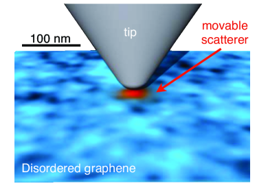
In this work, we use a liquid-He-cooled SPM tip to create a movable scatterer in a mesoscopic graphene Hall bar. As shown schematically in figure 2, a voltage-biased SPM tip is brought into close proximity with a graphene sample. Via capacitive coupling, the tip creates an image charge as a local change in the graphene charge density, indicated by the red spot, that adds to the average charge density controlled by a back gate voltage , and to the existing disorder in the graphene layer, shown in blue, which consists of randomly placed scatterers created by charged impurities located above or below the graphene sheet [34, 35]. As discussed below, the effect of the tip is to add one additional scatterer in the sample which can be moved about at will.
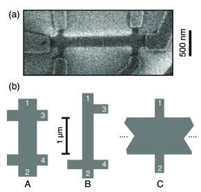
A scanning electron micrograph of a graphene sample is shown in figure 3a. The samples studied in these experiments are fabricated from single-layer graphene flakes deposited by mechanical exfoliation (the “sticky tape method”) on a degenerately doped Si substrate capped with 280 nm of SiO2. The samples were contacted by Cr/Au leads defined by electron beam lithography, and the graphene structures were formed by a mask defined by electron beam lithography followed by an oxygen plasma etch. A planar back gate voltage is applied between the sample and the conducting Si substrate, allowing us to tune the charge density in the graphene.
The data presented here are from three graphene samples, shown schematically in figure 3b; all showed the same qualitative behavior. Samples A and B were measured in a four-probe geometry, with lead 2 grounded, and a root-mean-square (rms) current nA at 5 kHz applied between leads 1 and 2; the voltage for conductance measurements was measured between leads 3 and 4, with a lock-in amplifier. Sample C was tested using a two-probe geometry with the same current applied between leads 1 and 2, with the voltage also measured across leads 1 and 2. For sample C, we estimate the contact resistance by finding the value of that fits the characteristic conductance expression vs. , which is linear on either side of the Dirac point ; similar data is shown below in figure 4a for the four-probe geometry. We find , which we subtract from the data from sample C.
Each sample is mounted in a home-built scanning probe microscope [24, 36], and cooled in He exchange gas that is in thermal contact with a liquid He bath at K. The sample sits in the core of a superconducting magnet that provides a magnetic field up to T perpendicular to the sample plane. We verify that the samples are single-layer graphene by observing quantum Hall conductance plateaux at the expected values of , where is an integer. For the scanning probe measurements, a conducting SPM tip with radius of curvature nm is held at a constant height nm above the graphene sample. The tip is grounded, so the tip charge is set by the contact potential between the graphene and the degenerately doped Si tip. Charged impurities on the surface of the graphene layer create image charges in the tip, which also contribute to the tip charge.
Using transport measurements and electrostatic simulations, we characterized our graphene samples, and determined the spatial profile of the density perturbation created by the SPM tip. Classical electrostatic simulations (Maxwell, Ansoft LLC) were used to determine the charge density profile in the graphene created by the back gate and the SPM tip. The back gate voltage capacitively creates a uniform charge density , with V-1cm-2, where is the offset of the Dirac point from caused by charged impurities near the graphene. The mobility for samples A, B, and C was cmVs, cmVs, and cmVs, found from the measured vs. curves. The local perturbation to the graphene charge density caused by the tip has a Lorentzian-like shape with half-width at half maximum (HWHM) nm, and a maximum cm-2 for a potential difference V between the tip and the sample. Previous experiments using scanning tunneling microscopy [37, 35] and a scanning single-electron-transistor charge sensor [29] have observed the disorder in graphene samples on a SiO2 substrate to consist of charge puddles with peak charge density cm-2 and lateral dimensions nm. The perturbation created by the tip in this paper has approximately the same amplitude as these naturally occurring charge density fluctuations, and about twice the width. Therefore, it is reasonable to think that the tip adds an additional, controllable scatterer to the pre-existing scatterers created by charged defects above and below the graphene.
4 Experimental Results
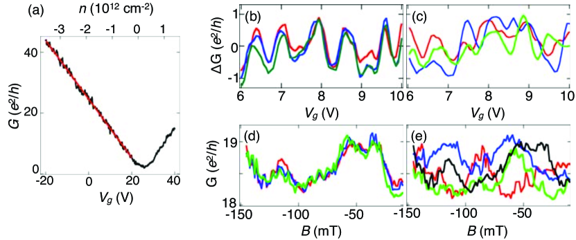
Using an SPM tip, we probe the dependence of coherent magnetotransport on the position of a single scatterer. Figure 4a shows the conductance of sample A vs. at zero magnetic field; the data vary linearly with on either side of the Dirac point V as indicated by the linear fit shown in red, as expected for single atomic layer graphene. The small fluctuations away from the linear fit are reproducible, and are attributed to UCF [16]. The fluctuations can be seen more clearly by subtracting the linear background from , as is shown over a small range of in figure 4b. The three traces of vs. repeat the same scan with the SPM tip fixed far from the sample (tip height m), demonstrating good reproducibility. The rms amplitude is in agreement theory [8, 9]. Figure 4c shows the effect of moving the charged SPM tip to three different positions spaced nm apart, at nm above the sample – the traces are now quite different. These data demonstrate that the motion of a single scatterer created by the SPM tip is sufficient to rearrange the conductance fluctuation pattern.
Moving the tip also changes fluctuations in the magnetoconductance . Figure 4d shows three traces of vs. with ( cm-2) and with the tip at three nearby positions, only 5 nm apart. Here the fluctuations repeat, with amplitude . In contrast, when the tip is moved to several locations spaced nm apart (figure 4e), the magnetoconductance is largely uncorrelated and looks like a different sample. Clearly, there is a critical length nm beyond which the tip must be moved in order to decorrelate the magnetoconductance fluctuations.
4.1 Conductance images and correlations in a magnetic field
We obtain conductance images by recording as the tip is raster scanning over a nm2 region in the center of the sample, at fixed magnetic field and back gate voltage . A conductance image consists of pixels that display the sample conductance over a two-dimensional array of tip positions with pixel spacing nm, as shown schematically in figure 5b. The standard deviation of the conductance in an image is given by the standard deviation of over all values of and . By acquiring a series of images as or is stepped to different values, we study the effect of the tip on coherent transport.
A series of conductance images vs. is shown in figure 5a with ( cm-2). The conductance images show fluctuations vs. with standard deviation and lateral sizes s of nm comparable to the Fermi wavelength and to the size of the scatterer created by the tip. The conductance images repeat over time intervals hr. as expected for coherent conductance fluctuations, demonstrating that their origin is not temporal noise. It can be seen by eye that the series of conductance images shown in figure 5a change with in a continuous fashion. We quantify this change by calculating the cross-correlation between conductance images and , where angle brackets denote the average over the tip position . We then define a normalized correlation , such that the autocorrelation of an image with itself is unity
| (5) |
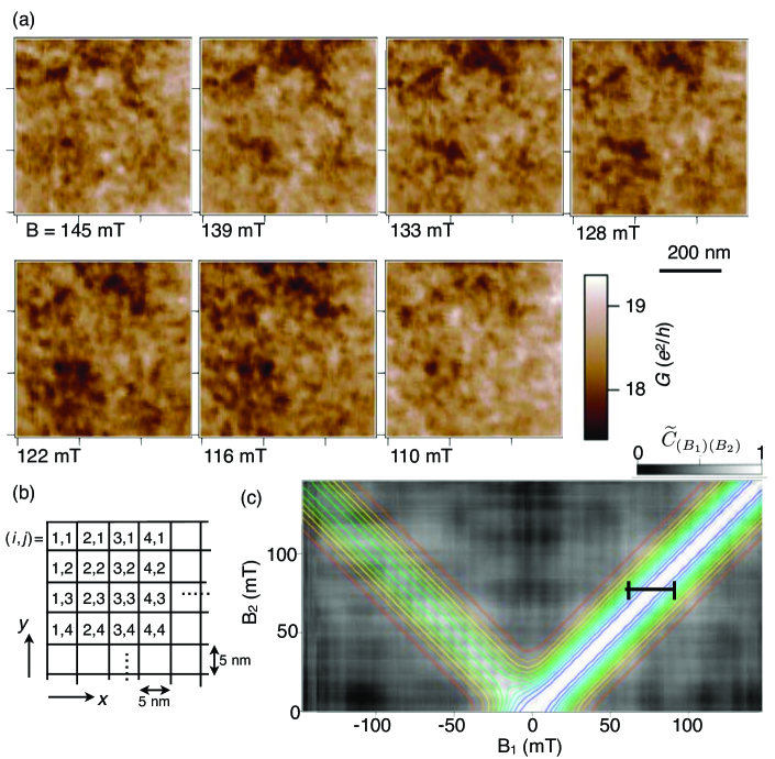
The grayscale map in figure 5c displays correlations between images and taken from a series of 200 images spanning mT at (as in figure 5a). By definition, . The fainter peak along shows that there is some symmetry in the magnetoconductance fluctuations as the sign of is reversed about . The symmetry is imperfect because of the nature of a coherent four-probe measurement [33], and because of slow drift of the images over the course of the measurement time hrs. We fit the map in figure 5c to a function given by the sum of two Gaussians centered at , shown as the contour plot in figure 5c. From this fit, we extract the magnetic correlation length mT, seen in figure 5c to be constant over the range of shown here; represents the magnetic field change needed to reduce the correlation between conductance images by one half. Using equation 4, we find the diffusive coherence length nm, where represents a value of obtained from . A series of images vs. provides a means to obtain and at a fixed back gate voltage , which we will return to below to study the behavior of vs. .
The amplitude of conductance fluctuations created by moving the local perturbation of the SPM tip differs from the amplitude created by changing the the global back gate voltage . This is understood by considering the ratio of the diffusive coherence length to the sample length [7]. A sample with width and length can be envisioned as uncorrelated, coherent regions in series, each with conductance and exhibiting coherent conductance fluctuations with standard deviation . The total conductance of the sample is
| (6) |
For a global change such as a change in , all regions undergo uncorrelated conductance fluctuations with standard deviation . The standard deviation in the total conductance is given by taking partial derivatives of equation 6 summed in quadrature:
| (7) |
Alternatively, the perturbation from the SPM tip acts locally, causing conductance fluctuations in only one coherent region yielding and for . For a local perturbation, the standard deviation in the total conductance is
| (8) |
We obtain the standard deviations and experimentally from conductance images and traces of vs. for sample A. To reduce the uncertainty, we average over 20 conductance images with back gate voltage stepped from to 1 V at yielding . We calculate from the standard deviation of conductance traces vs. in the same range of to 1 V, measured with the tip away from the sample and with the linear background subtracted, as in figure 4b. We find that the fluctuation created by the tip is smaller than that from the back gate voltage by the ratio . This value is in good agreement with theory, which predicts , using nm obtained above at .
4.2 Weak localization
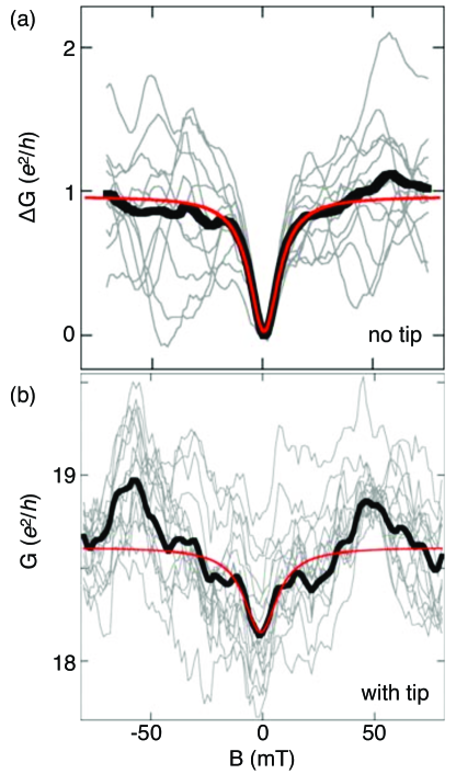
Weak localization can be identified by the conductance dip (or peak) that occurs at zero magnetic field. A conductance dip created by weak localization is shown in the magnetoconductance traces in figure 6. As for other measurements of exfoliated graphene [3, 4, 21], we observe a conductance dip from weak localization, not a peak. In our samples, where the sample size is comparable to , the conductance change from weak localization is comparable to that from UCF. To observe the weak localization effect alone, we average over multiple magnetoconductance traces, by varying either the density or the tip position to average out UCF.
We clearly observe the weak localization dip at in figure 6a, by averaging magnetoconductance traces at different densities with the tip away from the sample (m). The gray lines in figure 6a show a series of 11 magnetoconductance traces for densities stepped by cm-2 between cm-2 and cm-2, a range V. Because changes significantly with , these traces have been shifted to pass through the same point at . A weak localization dip is clearly seen in the average of all 11 traces, shown by the black curve, with magnetoconductance fluctuations averaged out.
We also observe the weak localization conductance dip in figure 6b by averaging magnetoconductance traces vs. over a grid of different tip positions . The gray lines show magnetoconductance traces at fixed cm-2 and different tip positions, on a grid spaced by nm, with nm. This data is obtained from a series of 200 conductance images at different magnetic fields , stepped from mT to mT. A magnetoconductance trace at tip position is extracted from the dataset by taking the same pixel from each image at different values of . The weak localization conductance dip is visible in the black curve in figure 6b, which is the average of all 6400 traces. Conductance fluctuations are still clearly visible in the averaged magnetoconductance, because the tip-created scatterer only affects the conductance in a region of size , about one third of the sample. Magnetoconductance fluctuations arising from regions of the sample at distances from the tip are not decorrelated by changing the tip position.
By measuring the width of the weak localization conductance dip shown in figures 6a and 6b, we obtain an estimate for the coherence length . To obtain , we fit the averaged curves of vs. in figures 6a and 6b to a Lorentzian function, which approximates the predicted lineshapes given in equations 2 and 3 for weak localization in two dimensions [7, 12]. The red lines in figures 6a and 6b show the results of the Lorentzian fit, with HWHM mT and mT in figures 6a and b respectively, in good agreement with each other. Using equation 1, we obtain a coherence length nm for figure 6a and nm for figure 6b. These values obtained from weak localization measurements match the estimate nm obtained above from cross-correlations between magnetoconductance images shown in figure 5.
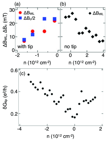
Measurements of from the weak localization conductance dip and measurements of from cross-correlations between conductance images allow us to study how the phase coherence length depends on the charge density . Previous bulk weak localization measurements found the coherence length in graphene varies significantly with , with a minimum at the Dirac point [4, 21]. Figure 7a shows our data for and vs. , obtained from conductance images for sample C. The agreement clearly shows the factor of 2 difference, predicted by the interference of two time-reversed diffusive loops for weak localization vs. the single loop for interfering forward scattering paths, discussed above. Each data point is derived from a series of 200 conductance images at a fixed density . The circles show , from the width of the weak localization conductance dip in an average over tip positions, as in figure 6b. The squares show obtained from the cross-correlation (equation 5) between conductance images and . We find from the correlation function as in figure 5c. The values of and in figure 7a both increase as the hole density decreases and the system approaches the Dirac point.
Figure 7b shows found for sample B with the tip fixed far from the sample. Each data point is obtained by averaging 20 magnetoconductance traces vs. over a range of densities cm-2 (a 5V change in ). The data in figure 7b show that increases as the electron density is decreased, and is largest at the Dirac point (), complementing the behavior for holes.
The coherence length for samples B and C is estimated from and in figures 7a and 7b, using equations 1 and 4. We find that the minimum coherence lengths nm occur at the Dirac point for both samples. The maximum coherence length occurs at the largest hole or electron density: nm for cm-2 in sample B, and nm at cm-2 in sample C. The change of with is in good agreement with previous results [4, 21], and is likely caused by the change in electron-electron interaction strength with [17, 4, 21], as well as the effects of electron-hole puddles near the Dirac point [22, 4, 21].
The standard deviation of conductance fluctuations over a single image for a series of conductance images at different densities at is shown in figure 7c. We find that increases away from the Dirac point with the electron or hole density; these results are similar to bulk transport measurements on single and multilayer graphene [19, 22, 38]. The trend in vs. is consistent with the behavior of and in figures 7a and 7b. As discussed above, when the sample length , then . Because and , we expect and ; the data in figure 7 follow this trend. From to cm-2, changes by a factor , which agrees with the observed change in and by a factor over the same range of in figures 7a and 7b.
5 Conclusions
The study of coherent electron transport and weak localization in graphene has recently received much attention through bulk transport measurements. Here, we add a new technique that allows one to probe transport by creating a movable scatterer with an SPM tip. This allows us to investigate weak localization in a new way by creating a controllable, local change to the disorder configuration. Our measurements provide a direct way to observe the spatial nature of coherent transport in graphene. This technique provides an image of the magnetoconductance vs. tip position that represents a spatial “fingerprint” of the interfering paths at a particular Fermi energy and magnetic field . From correlations between images at different we measure the coherence length for electrons diffusing through the sample, and find good agreement with the coherence length obtained from weak localization measurements.
Understanding and controlling disorder is one of the main challenges in realizing many of the proposals for probing new physics and discovering applications for graphene. In this work, we have described a tool that maps the effect of a nanoscale change to the disorder in a graphene sample produced by an SPM tip. This represents a step towards the goal of gaining mastery over disorder in graphene, by developing methods to controllably shape it and bend it to our will.
References
References
- Geim and Novoselov [2007] A. K. Geim and K. S. Novoselov. The rise of graphene. Nature Mat., 6:183–191, March 2007.
- Zhang et al. [2005] Y. Zhang, Y.-W. Tan, H. L. Stormer, and P. Kim. Experimental observation of the quantum Hall effect and Berry’s phase in graphene. Nature, 438:201–204, November 2005.
- Heersche et al. [2007] H. B. Heersche, P. Jarillo-Herrero, J. B. Oostinga, L. M. K. Vandersypen, and A. F. Morpurgo. Manifestations of phase-coherent transport in graphene - The Josephson effect, weak localization, and aperiodic conductance fluctuations. Eur. Phys. J. - Special Topics, 148:27–37, SEP 2007.
- Tikhonenko et al. [2008] F. V. Tikhonenko, D. W. Horsell, R. V. Gorbachev, and A. K. Savchenko. Weak localization in graphene flakes. Phys. Rev. Lett., 100(5):056802, 2008.
- Altshuler et al. [1980] B. L. Altshuler, D. Khmel’nitzkii, A. I. Larkin, and P. A. Lee. Magnetoresistance and Hall effect in a disordered two-dimensional electron gas. Phys. Rev. B, 22:5142–5153, December 1980.
- Bergmann [1984] Gerd Bergmann. Weak localization in thin films : a time-of-flight experiment with conduction electrons. Physics Rep., 107(1):1 – 58, 1984.
- Beenakker and van Houten [1991] C. W. J. Beenakker and H. van Houten. Quantum transport in semiconductor nanostructures. In H. Ehrenreich and D. Turnbull, editors, Solid state physics - Advances in research and applications, volume 44, pages 1–228. Academic Press Inc, San Diego, CA, 1991.
- Lee and Stone [1985] P. A. Lee and A. Douglas Stone. Universal conductance fluctuations in metals. Phys. Rev. Lett., 55(15):1622–1625, Oct 1985.
- Altshuler and Khmelnitskii [1985] B. L. Altshuler and D. E. Khmelnitskii. Fluctuation properties of small conductors. JETP Lett., 42(7):359, 1985.
- Washburn and Webb [1986] S. Washburn and R. A. Webb. Aharonov-Bohm effect in normal metal. Quantum coherence and transport. Advances in Physics, 35(4):375, 1986.
- Suzuura and Ando [2002] H. Suzuura and T. Ando. Crossover from symplectic to orthogonal class in a two-dimensional honeycomb lattice. Phys. Rev. Lett., 89(26):266603, Dec 2002.
- McCann et al. [2006] E. McCann, K. Kechedzhi, V. I. Fal’Ko, H. Suzuura, T. Ando, and B. L. Altshuler. Weak-Localization Magnetoresistance and Valley Symmetry in Graphene. Phys. Rev. Lett., 97(14):146805, October 2006.
- Rycerz et al. [2007] A. Rycerz, J. Tworzydlo, and C. W. J. Beenakker. Anomalously large conductance fluctuations in weakly disordered graphene. Europhys. Lett., 79(5):57003, 2007.
- Kharitonov and Efetov [2008] M. Yu. Kharitonov and K. B. Efetov. Universal conductance fluctuations in graphene. Phys. Rev. B, 78(3):033404, 2008.
- Kechedzhi et al. [2009] K. Kechedzhi, D. W. Horsell, F. V. Tikhonenko, A. K. Savchenko, R. V. Gorbachev, I. V. Lerner, and V. I. Fal’ko. Quantum transport thermometry for electrons in graphene. Phys. Rev. Lett., 102(6):066801, 2009.
- Berezovsky and Westervelt [2009] J. Berezovsky and R. M. Westervelt. Imaging universal conductance fluctuations in mesoscopic graphene. arXiv.0907.0428v1 [cond-mat], July 2009.
- Morozov et al. [2006] S. V. Morozov, K. S. Novoselov, M. I. Katsnelson, F. Schedin, L. A. Ponomarenko, D. Jiang, and A. K. Geim. Strong suppression of weak localization in graphene. Phys. Rev. Lett., 97(1):016801, 2006.
- Berger et al. [2006] C. Berger, Z. Song, X. Li, X. Wu, N. Brown, C. Naud, D. Mayou, T. Li, J. Hass, A. N. Marchenkov, E. H. Conrad, P. N. First, and W. A. de Heer. Electronic confinement and coherence in patterned epitaxial graphene. Science, 312(5777):1191–1196, MAY 26 2006.
- Graf et al. [2007] D. Graf, F. Molitor, T. Ihn, and K. Ensslin. Phase-coherent transport measured in a side-gated mesoscopic graphite wire. Phys. Rev. B, 75(24):245429, 2007.
- Wu et al. [2007] X. Wu, X. Li, Z. Song, C. Berger, and W. A. de Heer. Weak antilocalization in epitaxial graphene: Evidence for chiral electrons. Phys. Rev. Lett., 98(13):136801, 2007.
- Ki et al. [2008] D. Ki, D. Jeong, J. Choi, H. Lee, and K. Park. Inelastic scattering in a monolayer graphene sheet: A weak-localization study. Phys. Rev. B, 78(12):125409, 2008.
- Staley et al. [2008] N. E. Staley, C. P. Puls, and Y. Liu. Suppression of conductance fluctuation in weakly disordered mesoscopic graphene samples near the charge neutral point. Phys. Rev. B, 77(15):155429, 2008.
- Tessmer et al. [1998] S. H. Tessmer, P. I. Glicofridis, R. C. Ashoori, L. S. Levitov, and M. R. Melloch. Subsurface charge accumulation imaging of a quantum Hall liquid. Nature, 392:51–54, March 1998.
- Topinka et al. [2000] M. A. Topinka, B. J. LeRoy, S. E. J. Shaw, E. J. Heller, R. M. Westervelt, K. D. Maranowski, and A. C. Gossard. Imaging Coherent Electron Flow from a Quantum Point Contact. Science, 289:2323–2326, September 2000.
- Topinka et al. [2001] M. A. Topinka, B. J. LeRoy, R. M. Westervelt, S. E. J. Shaw, R. Fleischmann, E. J. Heller, K. D. Maranowski, and A. C. Gossard. Coherent branched flow in a two-dimensional electron gas. Nature, 410:183–186, March 2001.
- Topinka et al. [2003, and references therein] M. A. Topinka, R. M. Westervelt, and E. J. Heller. Imaging Electron Flow. Physics Today, 56(12):120000–52, December 2003, and references therein.
- Pioda et al. [2004] A. Pioda, S. Kičin, T. Ihn, M. Sigrist, A. Fuhrer, K. Ensslin, A. Weichselbaum, S. E. Ulloa, M. Reinwald, and W. Wegscheider. Spatially Resolved Manipulation of Single Electrons in Quantum Dots Using a Scanned Probe. Phys. Rev. Lett., 93(21):216801, November 2004.
- Jura et al. [2007] M. P. Jura, M. A. Topinka, L. Urban, A. Yazdani, H. Shtrikman, L. N. Pfeiffer, K. W. West, and D. Goldhaber-Gordon. Unexpected features of branched flow through high-mobility two-dimensional electron gases. Nature Phys., 3:841–845, December 2007.
- Martin et al. [2008] J. Martin, N. Akerman, G. Ulbricht, T. Lohmann, J. H. Smet, K. von Klitzing, and A. Yacoby. Observation of electron-hole puddles in graphene using a scanning single-electron transistor. Nature Phys., 4:144–148, February 2008.
- Braun et al. [2008] M. Braun, L. Chirolli, and G. Burkard. Signature of chirality in scanning-probe imaging of charge flow in graphene. Phys. Rev. B, 77(11):115433, 2008.
- Feng et al. [1986] S. Feng, P. A. Lee, and A. D. Stone. Sensitivity to the conductance of a disordered metal to the motion of a single atom: Implication for 1/f noise. Phys. Rev. Lett., 56(18):4, May 1986.
- Altshuler and Spivak [1985] B. L. Altshuler and B. Z. Spivak. Variation of the random potential and the conductivity of samples of small dimensions. JETP Lett., 42(9):447–450, NOV 10 1985.
- Ferry and Goodnick [1999] D. Ferry and S. M. Goodnick. Transport in Nanostructures. Cambridge University Press, October 1999.
- Rossi and Sarma [2008] E. Rossi and S. Das Sarma. Ground state of graphene in the presence of random charged impurities. Phys. Rev. Lett., 101(16):166803, 2008.
- Zhang et al. [2009] Y. Zhang, V. W. Brar, C. Girit, A. Zettl, and M. F. Crommie. Origin of spatial charge inhomogeneity in graphene. Nature Phys., 5(10):722–726, 10 2009.
- Aidala et al. [2007] K. E. Aidala, R. E. Parrott, T. Kramer, E. J. Heller, R. M. Westervelt, M. P. Hanson, and A. C. Gossard. Imaging magnetic focusing of coherent electron waves. Nature Phys., 3:464–468, July 2007.
- Deshpande et al. [2009] A. Deshpande, W. Bao, F. Miao, C. N. Lau, and B. J. LeRoy. Spatially resolved spectroscopy of monolayer graphene on SiO2. Phys. Rev. B, 79(20):205411, 2009.
- Horsell et al. [2009] D. W. Horsell, A. K. Savchenko, F. V. Tikhonenko, K. Kechedzhi, I. V. Lerner, and V. I. Fal’ko. Mesoscopic conductance fluctuations in graphene. Solid State Comm., 149:1041–1045, July 2009.