Effects of metallic contacts on electron transport through graphene
Abstract
We report on a first-principles study of the conductance through graphene suspended between Al contacts as a function of junction length, width, and orientation. The charge transfer at the leads and into the freestanding section gives rise to an electron-hole asymmetry in the conductance and in sufficiently long junctions induces two conductance minima at the energies of the Dirac points for suspended and clamped regions, respectively. We obtain the potential profile along a junction caused by doping and provide parameters for effective model calculations of the junction conductance with weakly interacting metallic leads.
pacs:
72.80.Vp, 73.40.Ns, 81.05.ue, 05.60.GgIntroduction. Graphene is a two-dimensional allotrope of carbon with atoms arranged in a honeycomb lattice. Successful fabrication of graphene monolayers by means of mechanical exfoliation of graphite Novoselov et al. (2004) or epitaxial growth on silicon carbide Berger et al. (2004) has ignited tremendous interest in this material Neto et al. (2009). Its favorable characteristics such as chemical inertness, low dimensionality, extremely high mobility, and easy control of carriers by applied gate voltages, along with patterning using nanolithography, open possibilities for further miniaturization of devices and the emergence of a carbon-based “post-silicon” electronics Berger et al. (2004); Avouris et al. (2007).
The electron transport at the nanometer scale is significantly affected by the contacts. The role of metallic leads in determining the transport properties of graphene-based junctions has been addressed by several theoretical Tworzydło et al. (2006); Robinson and Schomerus (2007); Blanter and Martin (2007); Golizadeh-Mojarad and Datta (2009); Nemec et al. (2008); Ran et al. (2009) and experimental Heersche et al. (2007); Lee et al. (2008); Huard et al. (2008); Danneau et al. (2008); Geim09 studies. Yet, a parameter-free description of transport in these systems is still lacking. Previously, the leads were modeled as infinitely doped graphene regions that support a large number of propagating modes Tworzydło et al. (2006). In this model, the important parameter is the ratio between the width () and length () of a junction: at the Dirac point, the universal, diffusive-like regime is reached for . Additional studies within a tight-binding approach have been reported, in which either the leads form a square lattice Robinson and Schomerus (2007); Blanter and Martin (2007), or the coupling to the leads is modeled via energy-level broadening Golizadeh-Mojarad and Datta (2009).
In this Letter, we report on large-scale first-principles calculations of electron transport in suspended graphene taking into account the effects of metallic leads. We study a non-magnetic junction made of graphene contacted underneath by two aluminum (Al) leads with a small in-plane mismatch of less than 1%. This junction is a prototype system with weak interaction between the metal contact and graphene, with no covalent bonds formed. Our work represents the first quantitative study of electron transport through metal-graphene junctions to examine in detail previous models Tworzydło et al. (2006); Golizadeh-Mojarad and Datta (2009) with dimensions relevant to experiment Heersche et al. (2007); Lee et al. (2008); Huard et al. (2008); Danneau et al. (2008), up to 100 nm wide and 13.6 nm long with various ratios.
The difference in the work functions of the metal and graphene leads to the charge transfer and doping of the graphene layer Giovannetti et al. (2008). We obtain the corresponding potential profile generated by the doping of the graphene layer along the junction. Not surprisingly, the potential in the region contacted by the metal starts deviating from its bulk value before reaching the geometrical edge. Finite doping results in specific transport features for long junctions: two conductance minima appear at the energies of the Dirac points of graphene in the clamped and suspended regions, respectively. For shorter junctions, where the two minima cannot be resolved, an electron-hole asymmetry in the conductance is still appreciable. The impact on transport of the orientation of graphene in the junctions is found to be negligible away from the Dirac point. Using the potential profile obtained from our first-principles calculations and a small energy broadening in the self-energies at the leads, we demonstrate that a -electron tight-binding model can accurately reproduce our first-principles transport results. This enables us to predict the conductance for graphene junctions with leads made of other metals, and we present results for the conductance of junctions with Au leads.
We perform transport calculations at zero source-drain bias using the nonequilibrium Green’s function (NEGF) SMEAGOL code Rocha et al. (2005), which is interfaced with the density-functional-theory (DFT) SIESTA package Soler et al. (2002). We employ norm-conserving pseudopotentials Troullier and Martins (1991) in the local-density approximation (LDA) Perdew and Zunger (1981), and a real-space grid equivalent to an energy cutoff of 310 Ry. We explicitly construct fine-tuned basis sets for C and Al atoms following the prescription of Junquera et al. Junquera et al. (2001). The largest number of atoms (numerical orbitals) included in the present calculations is 464 (5600). We made modifications to the transport code to improve memory allocation and parallelization, in order to handle calculations of this scale.

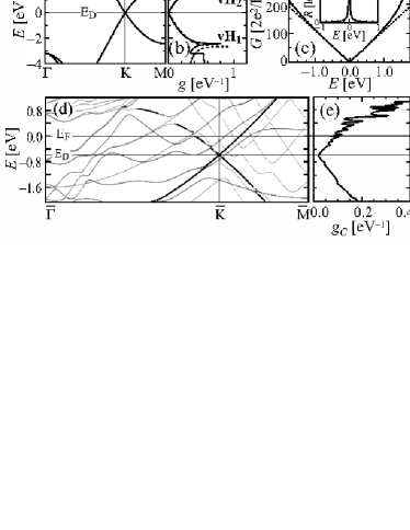
Graphene junctions without metal contacts. First we discuss pristine graphene with no metallic leads attached. The band structure and density of states (DOS) in the vicinity of the Dirac point () are shown in Figs. 1(a) and (b), respectively. The DOS around can be fitted to with /(eV2 unit cell). In all transport calculations described in this paper, an effective ribbon width is determined by , where is the number of -points used in the calculation and is the size of the unit cell in the transverse () direction. We show in Fig. 1(c) the conductance as a function of electron energy for a graphene ribbon of nm. At this width, the quantized plateaus in the conductance become unresolvable within the energy resolution employed (0.01 eV), and resembles the linear behavior of the DOS around . The boundary conditions and type of edge – zigzag or armchair – have an impact on the conductance only at the vicinity of the Dirac point, in a narrow energy range inversely proportional to the ribbon width. Away from , the conductance remains unaffected by this choice with being the same as the geometric width in the widest ribbons studied. Tight-binding results with a nearest-neighbor hopping parameter 2.65 eV determined from the LDA bandstructure are shown by dashed lines in Figs. 1(b) and (c) for comparison. The agreement with the DFT results is quite good within eV of the Dirac point.


Junctions with Al-graphene contacts. The electronic structure of graphene in contact with Al (henceforth referred to as the lead) shows a certain amount of hybridization arising from the interaction between graphene and the metal [Fig. 1(d)]. The leads are modeled by six layers of Al in the (111) orientation with a graphene monolayer placed at a distance of 0.34 nm away, in the minimal-energy configuration Giovannetti et al. (2008). Given the relative position of the Dirac point with respect to the Fermi level at the lead, eV, graphene becomes -doped in the contact region. The DOS projected on C atoms at the leads is nonzero at the Dirac point with a finite value of electrons/eV per graphene unit cell [Fig. 1(e)]. The fluctuations of above are due to hybridization.
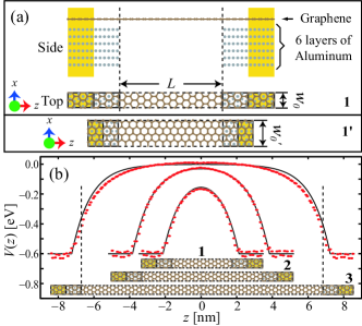
The junctions studied are schematically shown in Fig. 2. The leads are displayed within the shaded areas. The Hamiltonian, overlap, and density matrices of the leads are obtained self-consistently from DFT bulk-calculations and used to set up the electron density, chemical potential, and self-energies for the transport calculations. Since the leads include graphene, the contact area between metal and graphene is essentially infinite. This enhances the transparency Nemec et al. (2008), eliminating the large contact resistance that would arise if charge carriers were to tunnel from Al to graphene. An additional number of Al atoms between the leads and the freestanding section are added so that the self-consistent electrostatic potential across the junction develops smoothly. We have investigated various configurations to understand the effects of the length (), width (), and orientation of the graphene ribbon on electron transport. Junctions 1, 1’, 2 and 3 have lengths nm, nm, nm, and nm, respectively. The effect of varying is studied through junctions 1, 2, and 3 with a fixed width of nm [see Fig. 2(b) for geometries]; the conductance as a function of is studied for junction 1 ( nm); and the effect of ribbon orientation (armchair versus zigzag edges) is studied for junctions 1 and 1’ by choosing a similar width for them: nm (1) and nm (1’). (The potential profiles in Fig. 2(b) will be discussed later.)
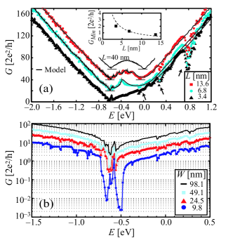
The conductance for junctions 1–3 (with a fixed width of nm) is shown in Fig. 3(a). One notices the lack of symmetry with respect to both the Fermi level (energy zero) and in the lead ( eV) in all cases regardless of the particular values of , in contrast to the symmetric curve for pristine graphene in Fig. 1(c) and those displayed in Ref. Tworzydło et al. (2006). Similar asymmetries in the conductance have been seen experimentally, e.g. Refs. Huard et al. (2008) and Farmer et al. (2009b). In addition to the conductance minimum at , the emergence of a second one at is apparent, and it becomes more prominent as the length increases. This is because, as , the electron DOS approaches at the freestanding part of the junction and the conductance becomes that of two resistors in series Farmer et al. (2009b): , where is the projected DOS of the clamped region. Based on the same underlying physics, a double peak in resistance was experimentally demonstrated for graphene devices comprising two regions with noticeably different doping levels Farmer et al. (2009a). The two conductance minima were also observed in junctions with gate-tunable barriers Others . The inset in Fig. 3(a) shows the minimal conductance near for the values of studied; it is of the order of . A small peak at ( eV) is visible for the two shorter junctions 1 and 2, and becomes unnoticeable for the longer junction 3. This small peak is due to states that exist only in the contact areas through hybridization with Al atoms and decreases rapidly with increasing junction length.
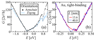
In Fig. 3(b) the conductance is plotted for the shortest junction ( nm) with four values of width : 9.8 nm, 24.5 nm, 49.1 nm, and 98.1 nm. The logarithmic scale of the conductance helps examine the linear dependence of the conductance on for energies sufficiently away from . As mentioned above, the peak at eV only appears in very short junctions. This is yet to be observed in experiment, where longer ribbons are customarily employed Han et al. (2007). Set aside this peak, the opening of a conduction gap with decreasing is evident, as well as the significant and nonlinear drop in conductance for the narrowest junction with nm, in full accordance with experiment Han et al. (2007). To investigate the effect of the edge orientation, we study the conductance of armchair (1) and zigzag (1’) junctions of comparable dimensions [Fig. 4(a)]. Only small deviations are found resulting from the anisotropy of the band structure. The effect of orientation is quite small in the vicinity of .
Tight-binding model. We next present a tight-binding model that can be used to study junctions bigger in size and with arbitrary nonbonding metal contacts. To that end, we estimate the effective potential profile at the atomic scale for -electrons along the junction, directly related to the spatial dependence of doping created by the metallic leads. This profile can be obtained semiclassically from DFT as the value of the energy at the Dirac point with respect to the Fermi level, as a function of : . We extract this quantity from the position-dependent energy shift of the van Hove singularities closest to the Dirac point [denoted by vH1 and vH2 in Fig. 1(b)] along the junction. The results for junctions 1–3 are shown in Fig. 2(b). Significant doping occurs at distances up to only a few nanometers from the edge of metallic leads. For the two longer junctions, 2 (6.80 nm) and 3 (13.60 nm), is very close to in the middle of the freestanding section (). We fitted our DFT results for by the following expression [solid lines in Fig. 2(b)]:
| (1) |
The parameters used are eV, nm and , where nm is the C-C interatomic distance. We emphasize that on the sub-nanometer scale, starts to deviate from its asymptotic value inside the region of intermediate Al atoms, before reaching the atomic boundary of the contact indicated by the vertical dashed line in Fig. 2(b). In our calculations, sufficiently many Al atoms are included between the bulk (shaded) leads and the freestanding section in order to map the transitional behavior of . This profile provides a refinement of models where sharp steps at the metal edge are assumed Tworzydło et al. (2006); Lee et al. (2008) and will become relevant as experimental junctions shrink in size.
We have performed conductance calculations within a tight-binding approach using the potential profile and a smearing meV introduced through the leads self-energies Golizadeh-Mojarad and Datta (2009) (to account for the nonzero conductance at and and the small peak at in Fig. 3). We obtain excellent agreement with our full-scale calculations [as indicated by the solid lines in Fig. 3(a)], with the exception of sharp dips in the conductance [indicated by arrows in Fig. 3(a)] which are not reproduced. These dips occur at the anticrossings energies due to hybridization with aluminum [cf. band structure in Fig. 1(d)]. We have also used the model to calculate the conductance for a longer junction ( nm), where the two conductance minimum are fully developed. In the limit only one conductance minimum appears and as a consequence the electron-hole symmetry is preserved Tworzydło et al. (2006).

Junctions with other nonbonding metal contacts. We use the model presented above to make a prediction for the conductance with Au as the metal lead. In this case eV and graphene is -doped Giovannetti et al. (2008). Using the same values of , in Eq. (1) and the smearing parameter as before, the conductance from tight-binding calculations is shown in Fig. 4(b) for two junctions with a fixed width of nm. The solid line shows results for nm and the dashed line for nm. For small values of , the two conductance minimum may be smeared out if the amount of charge fluctuations is significant Lee et al. (2008); Geim09 ; Rossi et al. (2009). Nevertheless, the electron-hole asymmetry should remain noticeable in the conductance curve. Our results give microscopic justification to prior theoretical studies where graphene junctions are modeled as an isolated graphene sheet with a space-dependent potential Tworzydło et al. (2006). However, we have demonstrated that to obtain accurate results, one needs to take into account a small energy broadening Golizadeh-Mojarad and Datta (2009) and allow for a finite potential at the contacts.
Conclusion. We have performed transport calculations for graphene junctions attached to Al leads using first-principles nonequilibrium Green’s function methods. The conductance features vary with the length and width of the junction, but are less sensitive to the ribbon orientation. We show that nonbonding metallic leads induce a noticeable electron-hole asymmetry in the conductance. The opening of a conduction gap with decreasing is also captured. Two minima in the conductance emerge for large enough junctions. In addition, our calculations yield reliable information on the doping variation along the junction for metallic leads interacting weakly with graphene, and we find accurate potential profiles at the vicinity of the metal boundary. We demonstrate that the dominant features of our first-principles results can be reproduced by an analytically tractable effective model. The parameters of the effective model are derived from first-principles. As an application we use the effective model to predict the conductance in junctions with Au as the supporting metal at the leads.
We thank L. Xian, K. Park, and E. Yepez for helpful discussions. This work is supported by the Department of Energy (Grant No. DE-FG02-97ER45632). We acknowledge interaction with the Georgia Tech MRSEC funded by the National Science Foundation (Grant No. DMR-02-05328) and computer support from Teragrid (TG-PHY090002) and NERSC.
References
- Novoselov et al. (2004) K. S. Novoselov, et al., Science 306, 666 (2004).
- Berger et al. (2004) C. Berger, et al., J. Phys. Chem. B 108, 19912 (2004); C. Berger, et al., Science 312, 1191 (2006).
- Neto et al. (2009) A. H. Castro Neto, et al., Rev. Mod. Phys. 81, 109 (2009); A. K. Geim, Science 324, 1530 (2009).
- Avouris et al. (2007) P. Avouris, Z. Chen, and V. Perebeinos, Nature Nano. 2, 605 (2007).
- Tworzydło et al. (2006) J. Tworzydło, et al., Phys. Rev. Lett. 96, 246802 (2006).
- Robinson and Schomerus (2007) J. P. Robinson and H. Schomerus, Phys. Rev. B 76, 115430 (2007).
- Blanter and Martin (2007) Y. M. Blanter and I. Martin, Phys. Rev. B 76, 155433 (2007).
- Golizadeh-Mojarad and Datta (2009) R. Golizadeh-Mojarad and S. Datta, Phys. Rev. B 79, 085410 (2009).
- Nemec et al. (2008) N. Nemec, D. Tománek, and G. Cuniberti, Phys. Rev. B 77, 125420 (2008).
- Ran et al. (2009) Q. Ran, et al., Appl. Phys. Lett. 94, 103511 (2009).
- Heersche et al. (2007) H. B. Heersche, et al., Nature (London) 446, 56 (2007).
- Lee et al. (2008) E. J. H. Lee, et al., Nature Nano. 3, 486 (2008).
- Huard et al. (2008) B. Huard, et al., Phys. Rev. B 78, 121402(R) (2008).
- Danneau et al. (2008) R. Danneau, et al., Phys. Rev. Lett. 100, 196802 (2008).
- (15) P. Blake, et al., Solid State Comm. 149, 1068 (2009).
- Giovannetti et al. (2008) G. Giovannetti, et al., Phys. Rev. Lett. 101, 026803 (2008); P. A. Khomyakov, et al., Phys. Rev. B 79, 195425 (2009).
- Rocha et al. (2005) A. R. Rocha, et al., Nature Materials 4, 335 (2005); A. R. Rocha, et al. Phys. Rev. B 73, 085414 (2006).
- Soler et al. (2002) J. M. Soler, et al., J. Phys.: Condens. Matter 14, 2745 (2002).
- Troullier and Martins (1991) N. Troullier and J. L. Martins, Phys. Rev. B 43, 1993 (1991).
- Perdew and Zunger (1981) J. P. Perdew and A. Zunger, Phys. Rev. B 23, 5048 (1981); D. M. Ceperley and B. J. Alder, Phys. Rev. Lett. 45, 566 (1980).
- Junquera et al. (2001) J. Junquera, et al., Phys. Rev. B 64, 235111 (2001).
- Farmer et al. (2009b) D. B. Farmer, et al., Nano Lett. 9, 388 (2009b).
- Farmer et al. (2009a) D. B. Farmer, et al., Appl. Phys. Lett. 94, 213106 (2009a).
- (24) B. Özyilmaz, et al., Phys. Rev. Lett. 99, 166804 (2007); J. R. Williams, L. DiCarlo, and C. M. Markus, Science 317, 638 (2007); B. Huard, et al., Phys. Rev. Lett. 98, 236803 (2007).
- Han et al. (2007) M. Y. Han, et al., Phys. Rev. Lett. 98, 206805 (2007); X. Wang, et al., Phys. Rev. Lett. 100, 206803 (2008).
- Rossi et al. (2009) J. Martin, et al., Nature Phys. 4, 144 (2008).