Electrical observation of a tunable band gap in bilayer graphene nanoribbons at room temperature
Abstract
We investigate the transport properties of double-gated bilayer graphene nanoribbons at room temperature. The devices were fabricated using conventional CMOS-compatible processes. By analyzing the dependence of the resistance at the charge neutrality point as a function of the electric field applied perpendicular to the graphene surface, we show that a band gap in the density of states opens, reaching an effective value of meV. This demonstrates the potential of bilayer graphene as FET channel material in a conventional CMOS environment.
The two dimensional arrangement of sp2-bonded carbon atoms, known as graphene, has attracted enormous attention since the group of Geim pushed it into the spotlight of the solid state community in 2004 Geim2004 . From a technological point of view the high mobility and the ampibolar character of charge carriers in graphene have attracted much interest and have led to investigations on using graphene as channel material for field-effect transistors (FET) Lemme ; Lin and opto-electronic devices Xia . However, as a zero band gap material the intrinsic on/off ratio of graphene based FETs is rather poor and not suitable for most applications. Therefore a major focus of research is on the investigation of opening a band gap in the density of states to increase the on/off ratio of graphene based FETs.
In bilayer graphene a tunable band gap can be introduced by a perpendicularly applied electric field. The electric field breaks inversion symmetry and introduces a band gap at the Dirac point reaching values of up to 300 meV McCann ; Castro . Although such a band gap could be observed by infrared spectroscopy Mak ; Zhang , the electrical measurement of such a gap is more sophisticated. As reported by Oostinga et al. an insulating state occurs in double-gated bilayer graphene, but only at cryogenic temperatures revealing an effective band gap size below 10 meV Oostinga . They proposed that inter-gap states induced by inhomogeneities in the local doping lead to a transport mediated via variable range hopping. Very recently F. Xia et al. Xia2 managed to detect a band gap in double-gated graphene by transport measurements at room temperature. By depositing a 9 nm thick organic layer directly on top of the graphene they could minimize inhomogeneities in the doping and thus reduce inter-gap states in the graphene. Our approach for reducing inhomogeneities in the doping concentration is confining the graphene layer to a nanoribbon. As recently shown by scanning gate microscopy micronscale inhomogeneities in the local carrier concentration with /cm2 are present in graphene layers Malcom . These inhomogeneities can be avoided by using nanoscale devices. In such small devices only smaller inhomogeneities with /cm2 are expected on a length scale of typically 20 nm Deshpande .
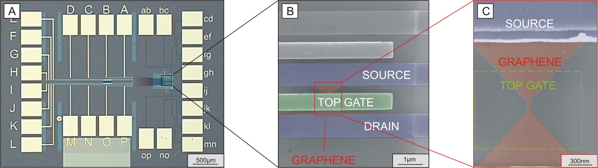
For investigating transport in bilayer graphene we fabricated double-gated graphene nanoribbons (GNRs) using standard CMOS-compatible processes. Bilayer graphene flakes were deposited by mechanical exfoliation from natural graphite on highly doped silicon substrates covered with 90 nm of thermal SiO2. Bilayer flakes were identified by their optical contrast to the substrate Blake . As back-gate electrode the highly p-doped substrate was used. In the first lithography step metal contacts were defined by means of electron beam lithography, thermal evaporation of 20 nm nickel and a subsequent lift-off. In the next step an etching mask for the nanoribbons was defined using e-beam lithography and PMMA as resist. The graphene etching was performed with an oxygen plasma. With this technique we were able to define nanoribbons with a width down to 30 nm uncovered by a resist, as PMMA can be removed after etching. An electron micrograph (false color) of a GNR having a width of 30 nm and a length of 250 nm is shown in figure 1C. After patterning the GNR the top-gate dielectric was deposited by thermal evaporation of nm SiOx and lift-off. The dielectric constant of the evaporated SiOx was measured using standard MOS-capacitors: . In the last step the top-gate electrodes were defined by e-beam lithography and thermal evaporation of 40 nm nickel followed by a lift-off process. A finished sample is depicted in figure 1 A-C. The top-gated bilayer GNRs presented in this paper have a width of 50 nm and a length of 250 nm. All measurements were performed at room temperature (295 K) in a needle probe station under nitrogen atmosphere. For probing a HP 4156B semiconductor parameter analyzer was used. Immediately before the measurement the sample was annealed for one hour in nitrogen atmosphere at 200 C to minimize contamination.
To investigate the opening of a band gap in bilayer graphene, the resistance of top-gated bilayer GNRs was measured as a function of the applied back-gate and top-gate voltage at a fixed source-drain voltage of 50 mV. In figure 2 the channel resistance of a top-gated bilayer GNR is depicted as a function of the applied top-gate voltage for different back-gate voltages ranging from V to 40 V. The measured resistance, in the presented device ranging from k to k, consists of the resistance of the active channel below the top-gate electrode and the resistance of the leads. As only the resistance of the active region is required for an analysis we subtracted the resistance of the relatively long and narrow leads which is in our case 12 k. This resistance was estimated using the lead geometry and the corresponding nickel resistivity and confirmed by a fit of the zero back-gate voltage transfer-trace similar to the one described in reference Kim .
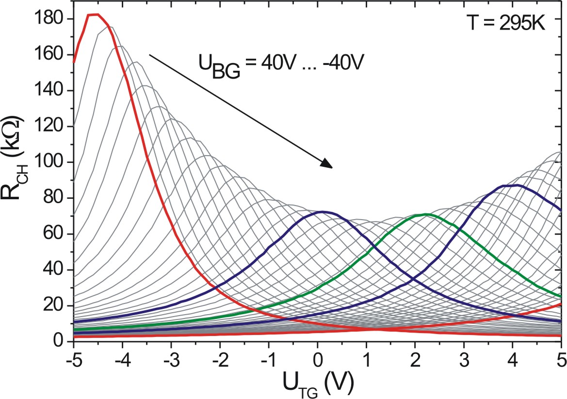
With this fit we also extracted a carrier mobility of 1000 cm2/Vs. At zero back-gate voltage (green trace in figure 2) the transfer characteristics show the typical behavior for bilayer graphene with an on/off ratio slightly below 10. The charge neutrality point is at a top-gate voltage of 2 V corresponding to a doping concentration of /cm2. The resistance at the charge neutrality point is 71 k, which translates into a sheet resistance of 6.2 k. With increasing back-gate voltage both, the resistance at the charge neutrality point and the on/off ratio increase, reaching values of 180 k and 80 at V respectively. These increases reveal the opening of a band gap in the density of states. The top-gate voltage at the Dirac point is plotted as a function of the applied back-gate voltage in the inset of figure 3 showing a perfect linear behavior as expected. From the slope the SiOx dielectric constant can be estimated to which is in good agreement with the estimated by using MOS-capacitors.
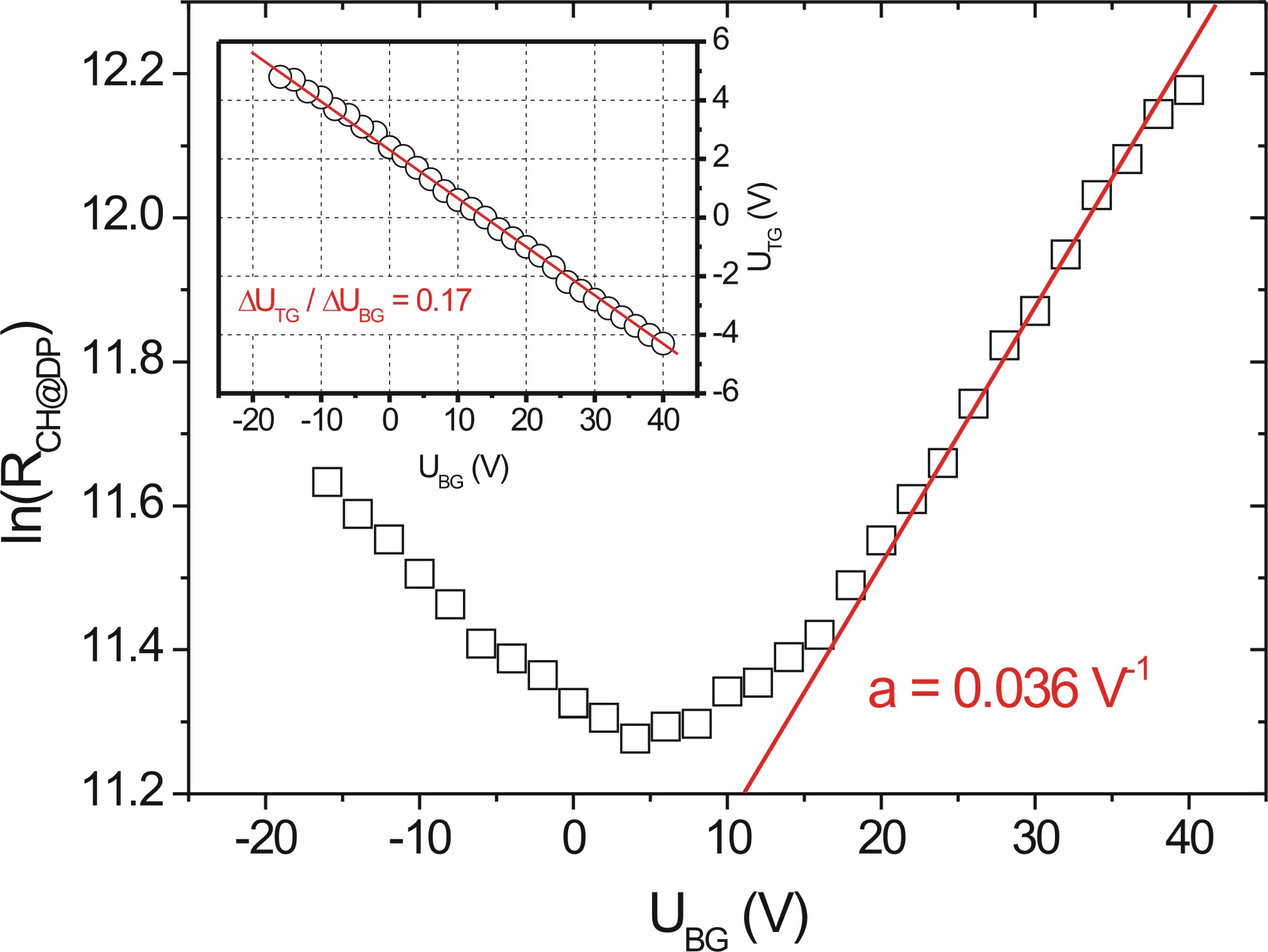
To analyze the opening of a band gap more quantitatively we plotted the logarithm of the channel resistance at the Dirac point as a function of the applied back-gate voltage in figure 3. In a semiconductor with the Fermi energy located inside the band gap the resistance depends on the temperature and the band gap energy by . Assuming that the band gap vanishes when is minimal, the band gap energy at V can be estimated by: meV. As indicated by the straight line in figure 3, the band gap energy scales roughly linearly for back-gate voltages from 15 V to 40 V, as one would expect for bilayer graphene at band gap energies smaller than 150 meV Zhang ; Mak . The average vacuum displacement field at the charge neutrality point is V/nm for V; here is the applied back gate voltage where is minimal. The estimated band gap energy is in fair agreement with the value reported by F. Xia et al. (80 meV at V/nm Xia2 ), but by a factor of four smaller than measrued optically Zhang . This difference can most likely be attributed to inter-gap states, which reduce the electric effective band gap, but do not alter the shape of the infrared spectroscopy signal. This explanation was already suggested by J.B. Oostinga et al. and confirmed by their analysis of the temperature dependency of the resistance at the charge neutrality point, showing an behavior at cryogenic temperatures, typical for variable range hopping Oostinga . We also investigated electric transport in two not-annealed top-gated bilayer GNRs having the same geometry as the device shown above. In these two devices the resistance at the charge neutrality point also increased with increasing back-gate voltage, but the effective band gap energy, estimated by the method shown in this paper, was only meV. This suggests that impurities removable by an annealing procedure are a major source of inter-gap states, which limit the effective band gap opening.
In summary, we have investigated transport in double gated bilayer graphene nanoribbons at room temperature. The resistance and on/off ratio of the investigated devices at the charge neutrality point increases with increasing displacement field showing that a band gap opens. The maximal achieved effective band gap energy was meV at V/nm in reasonable agreement with recent results obtained by Xia et al. in a different environment Xia2 , but four times smaller than calculated by theory and measured using infrared spectroscopy Zhang . This deviation between electrical and optical measurements in combination with the enhancement of the effective gap size by annealing shows that transport is still limited by randomly distributed inter-gap states introduced by contamination. Further attempts to increase the bandgap requires accurate control of the individual process steps to reduce parasitic contamination.
The authors would like to thank T. Wahlbrink and J. Bolten for performing the electron-beam lithography. This work was financially supported by the European Union under contract number 215752 (”GRAND”) and by the German Federal Ministry of Education and Research (BMBF) under contract number NKNF 03X5508 (”ALEGRA”).
References
- (1) K.S. Novoselov, A.K. Geim, S.V. Morozov, D. Jiang, Y. Zhang, S.V. Dubonos, I.V. Grigorieva, A.A. Firsov, Science 306, 666 (2004).
- (2) M.C. Lemme, T.J. Echtermeyer, M. Baus, and H. Kurz, IEEE Device Lett. 28, 282 (2007).
- (3) Y.-M. Lin, K.A. Jenkins, A. Valdes-Garcia, J.P. Small, D.B. Farmer, and P. Avouris, Nano Lett. 9, 422 (2009).
- (4) F. Xia, T. Mueller, Y.-M. Lin, A. Valdes-Garcia, and P. Avouris, Nature Nanotech. 4, 839 (2009).
- (5) E. McCann, Phys. Rev. B 74, 161403(R) (2006).
- (6) E.V. Castro, K.S. Novoselov, S.V. Morozov, N.M.R. Peres, J.M.B. Lopes dos Santos, J. Nilsson, F. Guinea F, A.K. Geim AK, and A.H.C. Neto, Phys. Rev. Lett. 99, 216802 (2006).
- (7) K.F. Mak, C.H. Lui, J. Shan, and T.F. Heinz, Phys. Rev. Lett. 102, 256405 (2009).
- (8) Y. Zhang, T.T. Tang, C. Girit, Z. Hao, M.C. Martin, A. Zettl, M.F. Crommie, Y.R. Shen, and F. Wang, Nature 459, 820 (2009).
- (9) J.B. Oostinga, H.B. Heersche, X.L. Liu, A.F. Morpurgo, and L.M.K. Vandersypen, Nature Phys. 7, 151 (2008).
- (10) F. Xia, D.B. Farmer, Y.-M. Lin, and P. Avouris, Nano Lett. DOI: 10.1021/nl9039636, online published January 2010.
- (11) M.R. Connolly, K.L. Chiou, C.G. Smith, D. Anderson, G.A.C. Jones, A. Lombardo, A. Fasoli, A.C. Ferrari, arXiv:0911.3832v1 (unpublished).
- (12) A. Deshpande, W. Bao, Z. Zhao, C. N. Lau, and B. J. LeRoy, Appl. Phys. Lett. 95, 243502 (2009).
- (13) P. Blake, E.W. Hill, A.H.C. Neto, K.S. Novoselov, D. Jiang, R. Yang, T.J. Booth, and A.K. Geim, Appl. Phys. Lett. 91, 063124 (2007).
- (14) S. Kim, J. Nah, I. Jo, D. Shahrjerdi, L. Colombo, Z. Yao, E. Tutuc, S.K. Banerjee, Appl. Phys. Lett. 94, 062107 (2009).