present address: ]Max-Planck-Institut für Chemische Physik fester Stoffe, D-01187 Dresden, Germany
Structure and giant magnetoresistance of granular Co-Cu nanolayers prepared by cross-beam PLD
Abstract
A series of CoxCu100-x ( = 0, 40…75, 100) layers with thicknesses in-between 13 nm and 55 nm were prepared on silicon substrates using cross-beam pulsed laser deposition. Wide-angle X-ray diffraction (WAXRD), transmission electron microscopy (TEM) and electrical transport measurements revealed a structure consisting of decomposed cobalt and copper grains with grain sizes of about 10 nm. The influence of cobalt content and layer thickness on the grain size is discussed. Electron diffraction (ED) indicates the presence of an intermetallic Co-Cu phase of Cu3Au structure-type. Thermal treatment at temperatures between 525 K and 750 K results in the progressive decomposition of Co and Cu, with an increase of the grain sizes up to about 100 nm. This is tunable by controlling the temperature and duration of the anneal, and is directly observable in WAXRD patterns and TEM images. A careful analysis of grain size and the coherence length of the radiation used allows for an accurate interpretation of the X-ray diffraction patterns, by taking into account coherent and non-coherent scattering. The alloy films show a giant magnetoresistance of 1…2.3 % with the maximum obtained after annealing at around 725 K.
pacs:
81.15.Fg, 68.55.Nq, 75.47.DeI Introduction
With the discovery of the giant magnetoresistance (GMR) effect in multi- Grünberg et al. (1986) and single-layer Xiao et al. (1992) systems, thin films of cobalt and copper have been investigated for basic research and applications Chen et al. (2008). The value of GMR, which varies between 1 % and 20 % in granular layers of Co and Cu, depends strongly on the preparation and post-process annealing. In addition to the electronic properties, these layers are also interesting from the structural point of view. Despite being isomorphic metals with quite similar lattice parameters (cobalt: space group , = 3.5446 Å; copper: , = 3.6148 Å Villars and Calvert (1985)) cobalt and copper are immiscible as bulk materials Massalski (1986). However, it is well known that thin layers can behave differently, especially when energetic deposition methods like pulsed laser deposition (PLD) are used. Thus, in addition to the decomposed Co and Cu grains Prieto et al. (2002) found in thin layers, a solid solution (mixed crystal) Pohorilyi et al. (1998) and evidence for an intermetallic alloy Yan et al. (2007) have been reported for Co-Cu systems. The use of cross-beam PLD (CB-PLD) for the preparation of alloy Fe-Cr nanolayers has led to the discovery of crystalline phases not reported before Gorbunov et al. (2002); Levin et al. (2002). Therefore, the aim of the present work was to show, whether the formation of metastable phases by using CB-PLD is also observable for Co-Cu layers.
We present a growth procedure, determine the lattice spacing and grain size, and discuss the effect of a post-process annealing on structure and magnetoresistance of Co-Cu nanolayers with different compositions.
II Experimental Procedure
II.1 Sample preparation
The Co-Cu alloy films were prepared by CB-PLD. A detailed description of this technique can be found in Ref. Gorbunoff (2002). CB-PLD allows the simultaneous and droplet-free deposition of two materials, in our case Co and Cu. In this technique, after ablation from two separated targets, the materials are mixed to variable proportions in the colliding laser plumes, thereby resulting in a mixed Co-Cu plume that is directed towards the substrate. Thermally oxidized (001) silicon wafers with a thickness of the amorphous silicon oxide layer of 500 nm were used as substrates. All depositions were performed at room temperature (RT) in a high vacuum (pressure mbar). A Nd:YAG laser with a wavelength of nm and an intensity of GW/cm2 at the target was used for the ablation. The repetition rate of the laser was 10 shots per second yielding an average film-deposition rate of nm/min on the substrate. In order to allow for uniform ablation, the target was rotated with a speed of rotations per second combined with a simultaneous periodic translation with a rate of 0.1 mm/s. The substrate was positioned at a distance of 10 cm from the target and 3 cm away from the origin of the resulting laser plume. In order to get a more homogeneous film, the substrate was rotated with a speed of rotation per second. By varying the ablation geometry, compositions of 40 % to 75 % cobalt could be realized. A preparation of Co-Cu alloy films containing more Cu is difficult because of the enhanced resputtering of Cu compared to Co. In addition, pure Co and Cu films were prepared.
A post-process anneal was carried out in a tubular furnace at temperatures from K up to K in steps of 25 K under high vacuum conditions ( mbar). After an anneal duration of 75 min, the samples were cooled down with an average rate of 10 K/min. A final thermal treatment was carried out at 750 K for 16 h in order to reach a stable state.
II.2 Characterization
The thickness of the deposited layers was determined by means of X-ray reflectometry to vary between 13 nm and 55 nm and did not change significantly after annealing. The lattice spacing and crystallite size of the Co-Cu films were determined by wide-angle X-ray diffraction (WAXRD) using a D8-Advance diffractometer (Bruker AXS) with Cu- radiation in divergent beam geometry. The Si 004 reflection was used as an internal standard for correcting angle reflection positions. A coupled (symmetric) - scan mode was used, where is the angle of the incident X-ray beam with respect to the surface, 2 is the angle between incident and reflected X-ray beam and = for the symmetric scan mode. Therefore, only lattice planes oriented parallel to the sample surface were taken into account in this scan mode. Asymmetric scan modes ( is fixed at a value corresponding to the maximum intensity of the respective rocking curve measured) did not show any influence on the X-ray reflection positions observed in the corresponding coupled scans. No additional WAXRD reflections were found by asymmetric scans.
The chemical composition of the layers was determined by means of energy dispersive X-ray spectroscopy (EDX) using a semiconductor detector (Noran Voyager 2000). Transmission electron microscopy (TEM) and electron diffraction (ED) measurements were made in a Zeiss EM 912 OMEGA microscope in order to determine structural parameters, homogeneity and grain size of the films. As transmission of the silicon substrate with the electron beam, or the removal of the deposited layer from the substrate, are impossible, a NaCl crystal was coated together with the substrate. After deposition of the Co-Cu layer, the NaCl crystal was dissolved in water and the Co-Cu layer was put onto a TEM mesh.
The electric transport measurements were performed at temperatures from 10 K to 300 K in magnetic fields up to T by using a VSM-Maglab cryostat (Oxford Instruments). The resistivity was measured by a standard 4-point contact method using conductive silver paint. In order to prevent silver contamination, some of the measurements were carried out using a simple 2-point contact method. A comparison of both techniques did not show significant differences. The characterization was performed because phases which are (meta)stable at ambient conditions were the focus of our investigations. Structure and composition did not change at ambient conditions over a period of one year.
III Results - as-prepared samples
III.1 Structural parameters obtained by WAXRD
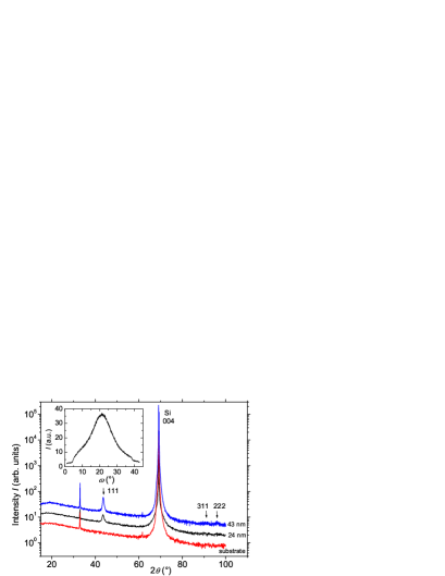
Typical WAXRD patterns of two characteristic as-prepared Co-Cu nanolayers with different thickness and composition are shown in Fig. 1. Note, in contrast to the known X-ray investigations on thin Co-Cu films from literature, our layers are rather thin. Due to the preferred orientation (fibre texture) and the small scattering volume of thin films, only a limited number of reflections are observable in the WAXRD patterns. Nevertheless, the WAXRD patterns show reflections not related to the substrate. For all CoxCu100-x compositions investigated, the non-substrate reflection with the highest intensity can be indexed as the 111 reflection of the face-centred cubic (fcc) Co-Cu lattice. The inset in Fig. 1 shows a rocking-curve around this reflection, revealing on the one hand that the texture is strong enough to inhibit the detection of other WAXRD reflections. On the other hand, the rocking curve is broad in comparison to an epitaxially grown layer or a single crystal and, therefore, the intensity of the scattered radiation (for a given -2 coupling) is low. These facts are responsible for the difficulties associated with using XRD for thin layers. Hence, a careful optimization of step width, sampling time and slits is necessary in order to obtain adequate results.
For layers with a thickness of less than 30 nm, only the 111 reflection of the face-centred cubic (fcc) lattice is observable (see second curve in Fig. 1 as an example). Nevertheless, the crystallographic structure of the layers is assumed to be similar to the structure of bulk fcc Cu and Co. This approach is supported by the fact that the observed (111) lattice spacing of pure Co and pure Cu layers is close to the values of the corresponding bulk materials. For the pure Co sample, the observed reflection can correspond either to the 111 reflection of the Co fcc structure or to the 0002 reflection of the Co hexagonal structure. Both structures are known to exist in thin cobalt layers Lamelas et al. (1989); Meny et al. (1992); Fauster et al. (1993). The upper pattern in Fig. 1 is a typical WAXRD pattern of a layer with a thickness of more than 40 nm in which weak 311 and 222 Co-Cu reflections are observed. Their low signal-to-noise ratio does not allow a quantitative analysis of the structural parameters. The lower pattern in Fig. 1 belongs to an uncoated silicon substrate. This shows that the substrate reflections are up to three orders of magnitude higher than those belonging to the Co-Cu nanolayers.
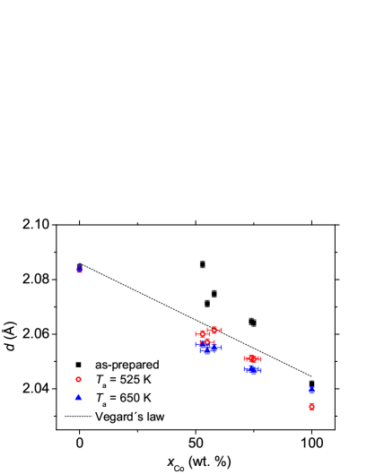
Instead of the individual 111 Cu and 111 Co reflections that would be expected due to the immiscibility of the deposited materials, one 111 fcc reflection is clearly observed in the WAXRD patterns of the Co-Cu layers. In general, this could be caused by the formation of a metastable Co-Cu solid solution or by size effects of the scattering crystallites. The determined (111) lattice spacing obtained for different CoxCu100-x compositions is shown in Fig. 2 together with Vegard’s law calculated for a hypothetic Co-Cu mixed crystal (see discussion). The strong deviation for the Co51Cu49 composition (as-prepared) from Vegard’s law, where the experimental lattice spacing is larger than that of pure copper, renders the existence of a solid solution very unlikely.
It should be noted, that any strain present in the crystallites in the film could contribute to the deviation observed. By assuming the absence of strain in films after annealing at temperatures higher than 525 K (see Fig. 2), the strain in as-prepared films was estimated from the lattice parameter change to be 0.5…1.5 %. An attempt to estimate the crystallite size in as-prepared films, based on these strain values, led to an unrealistic model of infinite crystallites (i.e. the strain was overestimated). Thus, the strain is significantly smaller than 0.5% and could not be evaluated accurately using the data obtained.
If strain is neglected, the crystallite size for CoxCu100-x films can be estimated by using the Scherrer equation
| (1) |
where is the full width at half maximum (FWHM) of the WAXRD reflection. In order to take into account the instrumental broadening caused by the experimental setup, the observed FWHM () of the WAXRD reflection was corrected by using the FWHM of the silicon 004 substrate reflection (). Since for all reflections ( is the integral breadth of the reflection), the reflection profiles could be described as Lorentzians Langford (1980). Following the procedure described in Warren (1990) for X-ray reflections of Lorentzian profile shape, the reflection FWHM was corrected by
| (2) |
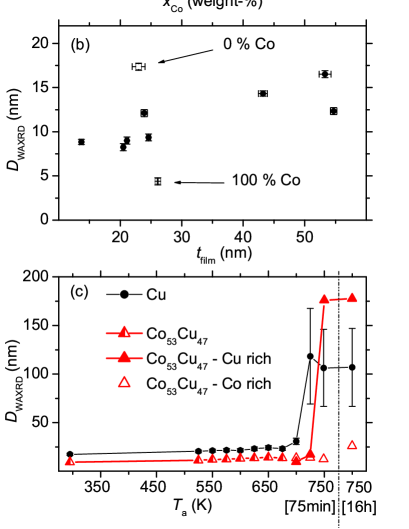
The crystallite sizes () obtained for different compositions, together with the grain size obtained by TEM (, see next paragraph), are shown in Fig. 3(a). The crystallite/grain size does not exceed the thickness of the layers. We measured the thickness of the sample containing 53 % Co to be 25 nm, whereas the thickness of the sample containing 55 % Co is only 13 nm. Nevertheless, their crystallite sizes are very similar (Fig. 3(a)), which shows that the crystallite size is more strongly affected by the Co content than by the layer thickness. However, there is a weak correlation between layer thickness and crystallite size observable (Fig. 3(b)). Within the accuracy of our measurements the crystallite/grain sizes of the alloy systems lie between the grain sizes of the pure compounds.
III.2 Transmission electron microscopy
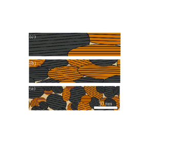
Another approach used to measure the crystal grain sizes was TEM. The dark grains in the TEM micrographs (Fig. 4) fulfill the Bragg condition, i.e. the contrast is not induced by absorption differences. The grain size was determined by averaging the size of 20 randomly chosen grains. These are shown in Fig. 3(a) as a function of cobalt content. It should be noted that the grain size determined by TEM is in most cases not the same quantity as the crystallite size obtained by WAXRD. The grains can contain more than one crystallite. As can be seen in Fig. 3(a), for all alloy compositions, the size of crystallites and grains determined by WAXRD and TEM, respectively, are equal in the limits of the estimated standard deviations (e.s.d.). This highlights the equivalence of the crystallite and grain sizes for the deposited alloy CoxCu100-x nanolayers. At the same time, the grain sizes of the pure Co and Cu films are about two to three times larger than the crystallite sizes, indicating the formation of large grains containing 2-3 crystallites.
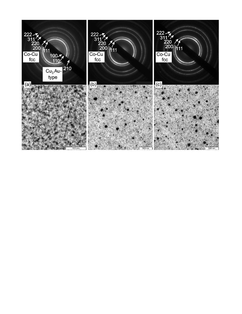
ED-patterns (Fig. 4(a)) show the Bragg reflections which can be well indexed using an fcc lattice in agreement with the WAXRD patterns. Three additional reflections violating the extinction law of the fcc lattice were found for all compositions (as-prepared films). The assumption of an additional intermetallic phase of Cu3Au-type and unit cell parameter Å, theoretically predicted by Yan Yan et al. (2007), is in good agreement with the experimental data. As the Cu3Au structure-type is a superstructure of the fcc lattice, the similar atomic scattering factors of Co and Cu cause a weak intensity of the 100, 110 and 210 Bragg reflections which cannot be resolved by WAXRD. However, the different substrate (NaCl) also could be responsible for the occurrence of these phases compared to the case of the WAXRD investigated layers on amorphous silicon oxide substrates.
III.3 Electrical transport measurements – giant magnetoresistance
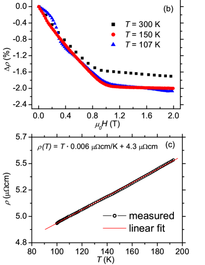
The electrical transport measurements are shown in Fig. 5 for nanolayered Co59Cu41 (as-prepared). The development of the electrical resistance at RT as a function of applied magnetic field is shown in Fig. 5(a) for two different orientations of the field. The change in the resistivity is defined as
| (3) |
For a magnetic field oriented perpendicular to the surface and thus perpendicular to the electrical current, the resistivity rapidly decreases by % at T followed by a moderate decrease to % at T. This decrease is most likely caused by the GMR effect, because the anisotropic magnetoresistance (AMR) exhibits a smaller decrease in the resistivity and smaller saturation fields. Literature values for a pure Co layer prepared by PLD are %, with a saturation field of T Krieger (2004). The stronger GMR for a magnetic field aligned perpendicular to the surface is a thin film phenomenon and/or caused by the texture (the granular GMR should be isotropic). Even for high fields T no saturation is observed, which is typical for the GMR in granular layers.
For the following measurements, the magnetic field was applied perpendicular to the surface. Magnetic field dependencies of the GMR effect at RT and lower temperatures are shown in Fig. 5(b). Up to an applied magnetic field of T, at RT and low temperature the resistivity change shows approximately the same magnitude. However, the low temperature (150 K and 107 K) resistivity continues to decrease with the same rate up to a magnetic field of T reaching % with a further moderate decrease to % at T. At a temperature of K, shows oscillations around the smoothly decreasing GMR curve measured at K. However, the temperature was no less stable in this case. We have no explanation for this effect.
The temperature dependence of the electrical resistance in zero magnetic field clearly shows a metal-like behavior (Fig. 5(c) for temperatures between 100 K and 200 K with an extrapolated residual resistivity of 4.3 cm).
IV Results – Influence of thermal treatment
IV.1 Development of structural parameters observed by XRD
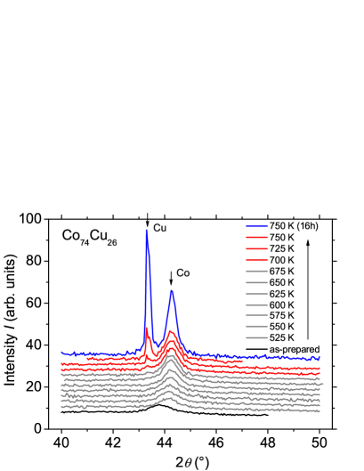
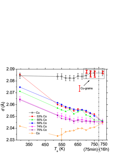
The development of the X-ray diffraction pattern due to thermal treatment is shown in Fig. 6. The corresponding lattice spacings are shown in Fig. 7, where the monotonic decrease of the lattice spacing of the CoxCu100-x alloy nanolayers with increasing annealing temperature for K and for Co-rich grains to higher temperatures is apparent (see solid symbols for alloy compositions in Fig. 7). As a result of annealing process, the interplanar distances of the CoxCu100-x alloy nanolayers show a better agreement with Vegard’s law, with values slightly smaller than could be expected from the law (see Fig. 2 as an example for annealing at K and K). These results show that it is also possible to adjust the (average) (111) lattice spacing of the material system Co-Cu with sub-picometre precision by using a thermal treatment.
The development of the lattice spacing belonging to copper-rich grains is shown in the upper right part of Fig. 7, where all measured values are within the thick (red) bars. The corresponding WAXRD reflection, appearing after a thermal treatment at 425 K (Fig. 6), does not undergo a significant change in 2 for the last four thermal treatments but its intensity does. The lattice spacing calculated for this reflection corresponds to pure copper, where the presence of copper has been verified by selected area EDX. The two resulting reflections formed after the final thermal treatment belong to pure cobalt and pure copper. Fig. 3(c) shows the development of the crystallite size as a function of the annealing temperature for a pure copper sample and for Co53Cu47. Up to K the crystallite size shows a moderate increase with increasing temperature. This is followed by a significant growth of Cu-rich crystallites after higher temperature anneals, where the individual reflections of Co- and Cu-rich grains are formed (see Fig. 6).
Note that after annealing at temperatures higher than 425 K, the crystallite/grain sizes determined by WAXRD and TEM exceed the film thickness. However, this possible contradiction is resolved taking into account that only lateral grain size is accessible by TEM. In the case of WAXRD, the calculated crystallite size is a mean effective quantity averaging the crystallite sizes in different directions.
IV.2 Thermal treatment during TEM investigations
An additional thermal treatment test was performed in the TEM for temperatures between 450 K and 600 K. After 15 min anneal, a bright field image and an ED pattern were taken after the sample had cooled down to RT. An increase of the grain size during the thermal treatment is observable from the lower part of Fig. 4. The dark regions, with a size of about 100 nm, belong to grains of pure copper, as verified by selected area EDX. Similar values for the crystallite sizes of Cu-rich grains after annealing are obtained by XRD using the Scherrer equation (Fig. 3(c)). In the upper part of Fig. 4 the corresponding ED patterns are shown. It can be seen that the additional rings, which do not belong to the fcc lattice, and are attributed to an intermetallic phase of Cu3Au structure-type (see Sec. 3.2), disappear completely during the thermal treatment.
IV.3 Influence of thermal treatment on the GMR
No direct correlation between the composition of the as-prepared or annealed layers and the magnitude of the GMR effect was found for the samples investigated in this paper.
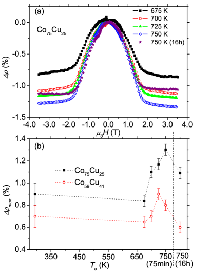
The change of the GMR effect after a thermal treatment is shown in Fig. 8(a) for a nanolayer with composition Co75Cu25. The effect increases for anneals of up to 750 K for 75 min. Further annealing at 750 K for 16 h leads to a decrease of the effect. Fig. 8(b) shows the maximum change of the electrical resistivity as a function of the annealing temperature for two samples with characteristic compositions of 59 % Co and 75 % Co, and a film thickness of about 20 nm. Both samples show a maximum in the GMR effect after annealing at K. The magnitude of the GMR effect after a thermal treatment is a factor of larger than the as-prepared samples. This change is rather weak compared to other results published which show comparable values for the as-prepared samples Errahmani et al. (2000); Jackson et al. (1996). However, the layer thickness was nm and nm Errahmani et al. (2000); Jackson et al. (1996), and annealing led to an enhancement of the GMR by a factor of and , respectively. This suggests the grain size perpendicular to the electrical current plays an important role. A second possible reason for the comparatively small GMR in our case is the large cobalt content well above the percolation threshold.
V Discussion
All investigated as-prepared Co-Cu layers exhibit only one significant Bragg reflection and possess a GMR effect at the same time. Similar observations were published several times, see e.g. Errahmani et al. (2000). These two points are contradictory because ferromagnetic grains separated by a non-magnetic spacer, i.e. two separate phases, are necessary for the occurrence of the GMR effect. However, for this case, at least two Bragg reflections of two different crystalline phases, namely one for Co and one for Cu, would be expected in the WAXRD pattern, which was not the case. Furthermore, the development of the diffraction pattern after the thermal treatments (Fig. 6) could be misinterpreted as a decomposition of an initial solid solution into grains of pure Co and pure Cu.
These discrepancies can be solved by taking into account that the grain size of nm is smaller than the coherence length of the used X-ray radiation. The lateral coherence length of the X-ray radiation can be estimated using the equation Attwood (1999) ), where Å is the wavelength used, m is the distance between the X-ray source and sample, and mm is the X-ray focus spot size (Bruker KFL-Cu-2K tube). From the equation nm is calculated. Therefore, a coherent superposition of X-ray waves scattered by Co grains and Cu grains, results in only one Bragg reflection in the diffraction pattern (i.e. the scattered amplitudes of Co and Cu are added but not their squares Meyer and Paufler (2000)). This leads to the misinterpretation of the existence of a solid solution (mixed crystal) in the Co-Cu layer. During the thermal treatment, the increase of grain size leads to the development of two Bragg reflections of Co- and Cu-rich phases in the WAXRD pattern as soon as the grain size exceeds the coherence length of the radiation. This is supported by TEM results which show copper grains larger than 100 nm (lower panel in Fig. 4(b)). Furthermore, the size of the copper crystallites is estimated to be larger than 100 nm using the Scherrer equation (Fig. 3(c)) with the FWHM of the developing 2nd Bragg reflection attributed to pure Cu (Fig. 6, K, left WAXRD reflection). Therefore, the change of lattice spacings shown in Fig. 7 is not an intrinsic property of the Co-Cu layers but is caused by a complex change of the interference conditions due to increasing grain size. As a matter of fact, the lattice spacing of Co- and Cu-grains in the alloy films does not change significantly during the annealing process, similar to the lattice spacing of single phase Co- and Cu-films.
A model of the real structure of Co-Cu nanolayers and their development after thermal treatment is schematically represented in Fig. 9. The as-prepared film material consists of fine Co- and Cu-grains which are smaller than the coherence length of the X-ray radiation as supported by TEM and WAXRD measurements. As a result, the WAXRD patterns exhibit only one Bragg reflection, the electrical resistivity measurements reveal the presence of the GMR effect. Thermal treatment leads to an increase of the grain size and enhanced GMR values. When the (lateral) grain size reaches the coherence length of the X-ray radiation (Fig. 9(b)), a second Bragg reflection is observed which corresponds to the lattice spacing of pure copper. Annealing at higher temperatures results in a further increase of (lateral) grain size (Fig. 9(c)) and an increase in GMR effect. However, prolonged annealing at high temperatures results in a decrease of GMR (Fig. 8(b)), which could be caused by an enhanced spin-flip scattering inside larger crystallites Mathon (2001). Finally, for higher annealing temperatures, two distinct Bragg reflections occur in WAXRD patterns and large Cu grains become visible in the TEM bright field images.
VI Conclusions
The as-prepared film material consists of fine Co- and Cu-grains with typical sizes smaller than the coherence length of the X-ray radiation (Cu-) used. This gives an explanation for the occurrence of the GMR effect in as-prepared and annealed films, even though X-ray diffraction patterns show only one Bragg reflection. The size of crystallites in films is more strongly affected by the Co content than by the layer thickness. No intermetallic alloy was found in as-prepared and annealed Co-Cu films on silicon substrates using WAXRD. However, indications for an intermetallic alloy of Cu3Au structure-type in as-prepared Co-Cu films were observed in ED-patterns, showing that this phase exists, as theoretically predicted in Yan et al. (2007). Annealing of the samples results in the growth of larger Co- and Cu-rich grains and a larger GMR effect. However, the appearance of larger GMR values is assumed to be restricted by the small grain size perpendicular to the electrical current, i.e. by the layer thickness.
VII acknowledgment
The authors would like to thank M. Dörr and S. Granovsky for help with electrical transport measurements and R. Boucher for valuable discussions.
References
- Grünberg et al. (1986) P. Grünberg, R. Schreiber, Y. Pang, M. B. Brodsky, and H. Sowers, Phys. Rev. Lett. 57, 2442 (1986).
- Xiao et al. (1992) J. Q. Xiao, J. S. Jiang, and C. L. Chien, Phys. Rev. Lett. 68, 3749 (1992).
- Chen et al. (2008) Y. Chen, Y. Mei, R. Kaltofen, J. I. Mönch, J. Schumann, J. Freudenberger, H. J. Klauß, and O. G. Schmidt, Adv. Mater. 20, 3224 (2008).
- Villars and Calvert (1985) P. Villars and L. D. Calvert, Pearson s Handbook of Crystallographic Data for Intermetallic Phases, vol. 2 (ASM International, 1985).
- Massalski (1986) T. B. Massalski, Binary Alloy Phase Diagrams (ASM International, 1986).
- Prieto et al. (2002) A. G. Prieto, M. L. Fdez-Gubieda, C. Meneghini, and A. Garcia-Arribas, J. Appl. Phys 91 (2002).
- Pohorilyi et al. (1998) A. N. Pohorilyi, A. F. Kravetz, E. V. Shipil, A. Y. Vovk, C. S. Kim, and H. R. Khan, J. Magn. Magn. Mater. 186, 87 (1998).
- Yan et al. (2007) H. F. Yan, Y. X. Shen, H. B. Guo, and B. X. Liu, J. Phys.: Condens. Matter 19, 026219 (2007).
- Gorbunov et al. (2002) A. Gorbunov, A. A. Levin, A. Mensch, D. C. Meyer, A. Tselev, P. Paufler, W. Pompe, and D. Eckert, Appl. Surf. Sci. 197, 475 (2002).
- Levin et al. (2002) A. A. Levin, D. C. Meyer, A. Gorbunov, A. Tselev, W. Pompe, and P. Paufler, J. Alloys Compd. 347, 171 (2002).
- Gorbunoff (2002) A. Gorbunoff, Laser-Assisted Synthesis of Nanostructured Materials (VDI Verlag, 2002).
- Lamelas et al. (1989) F. J. Lamelas, C. H. Lee, H. He, W. Vavra, and R. Clarke, Phys. Rev. B 40, 5837 (1989).
- Meny et al. (1992) C. Meny, P. Panissod, and R. Loloee, Phys. Rev. B 45, 12269 (1992).
- Fauster et al. (1993) T. Fauster, G. Rangelov, J. Stober, and B. Eisenhut, Phys. Rev. B 48, 11361 (1993).
- Langford (1980) J. Langford, Accuracy in Powder Diffraction (Natl Bur. Stand. Spec. Publ. No 567, 1980).
- Warren (1990) B. Warren, X-ray Diffraction (Courier Dover Publications, 1990).
- Krieger (2004) M. Krieger, Herstellung magnetischer Multilagen mit gepulster Laserablation - Charakterisierung durch elektrischen Transport (Dissertation, Ulm, 2004).
- Errahmani et al. (2000) H. Errahmani, A. Berrada, G. Schmerber, and A. Dinia, Vacuum 56, 221 (2000).
- Jackson et al. (1996) T. J. Jackson, S. B. Palmer, H. J. Blythe, and A. S. Halim, J. Magn. Magn. Mater. 159, 269 (1996).
- Attwood (1999) D. Attwood, Soft X-Rays and Extreme Ultraviolet Radiation (Cambridge University Press, 1999).
- Meyer and Paufler (2000) D. C. Meyer and P. Paufler, J. Alloys Comp. 298 (2000).
- Mathon (2001) J. Mathon, Lecture Notes in Physics, 569 (Springer, 2001).