The Planck/LFI Radiometer Electronics Box Assembly
Abstract
The Radiometer Electronics Box Assembly (REBA) is the control and data processing on board computer of the Low Frequency Instrument (LFI) of the Planck mission (ESA). The REBA was designed and built incorporating state of the art processors, communication interfaces and real time operating system software in order to meet the scientific performance of the LFI. We present a technical summary of the REBA, including a physical, functional, electrical, mechanical and thermal description. Aspects of the design and development, the assembly, the integration and the verification of the equipment are provided. A brief description of the LFI on board software is given including the Low-Level Software and the main functionalities and architecture of the Application Software. The compressor module, which has been developed as an independent product, later integrated in the application, is also described in this paper. Two identical engineering models EM and AVM, the engineering qualification model EQM, the flight model FM and flight spare have been manufactured and tested. Low-level and Application software have been developed. Verification activities demonstrated that the REBA hardware and software fulfil all the specifications and perform as required for flight operation.
keywords:
Cosmic Microwave Background – space mission – Data Handling - Digital Signal Processing - Data Compression – Data Acquisition - Low-Level Software – SpaceWire - MIL-STD-1553B1 Introduction
The Low Frequency Instrument (LFI, Bersanelli et al. 2009; Mandolesi et al. 2009) of the ESA satellite Planck consists of an array of 11 corrugated horns feeding 22 polarisation sensitive pseudo-correlation radiometers based on HEMT transistors and MMIC technology. These are actively cooled down to 20 K by using a new concept sorption cooler. The radiometers cover three frequency bands centred at 30 GHz, 44 GHz, and 70 GHz. The LFI shares the focal plane of the 1.5m-aperture Planck telescope with the High Frequency Instrument (HFI), which is based on bolometric detectors cooled to 0.1 K (Lamarre et al. 2009). The combination of LFI and HFI is designed to provide full-sky maps of the microwave sky with an unprecedented combination of spectral coverage (30-850 GHz), sensitivity (), angular resolution ( arcmin) and suppression of systematic effects.
Each LFI radiometer correlates the signal from the sky with that of a reference blackbody source cooled to 4 K. At the end of the radiometric chain, the amplified signals are detected by square law diodes, DC amplified and transmitted to the Data Acquisition Electronics (DAE) for signal conditioning and digitization.
The LFI array required a dedicated electronic system to perform on-board instrument control, command and data handling as well as the on-board scientific data processing with high reliability and robustness. These functions are carried out by the LFI Radiometer Electronics Box Assembly (REBA), which is described in detail in this paper. In particular, the REBA incorporates the compression algorithms needed to optimize the use of the satellite to ground available communication bandwidth. The expected output of LFI is 5.7 Mbps while the available effective bandwidth is the order of 53 kbps, implying a need for on board pre-processing of the raw data. The most relevant physical, functional, electrical, mechanical and thermal characteristics of the REBA, as well as the main software aspects, are described in detail in the following sections. For a broad description of the REBA in the context of LFI, see Section 4.4.2 in Bersanelli et al. (2009) on the DAE and its connection with REBA.
2 Equipment overview
The REBA is a warm electronics unit consisting of two separate identical units, one nominal and one redundant, which operate in cold redundancy under power supply control of the spacecraft. Each unit has an envelope of mm3, is painted in mat black with an emissivity of 0.9, and weights 4.32 Kg (see Figure 1). The measured power consumption of the REBA is 22.7 W fully running and processing science data, while the measured total power consumption of LFI is 68.3 W. Each unit houses three stacked electronics modules and they are located on the lateral panels of the service module (SVM) of the spacecraft at about 300 K.
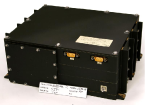
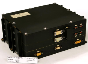
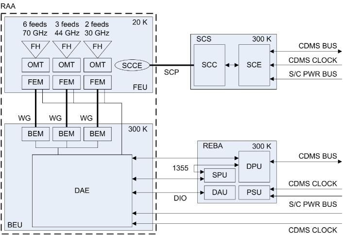
Each REBA unit is connected to the instrument Data Adquisition Electronics (DAE) in the Radiometer Array Assembly (RAA) through the instrument harness and to the spacecraft Central Data Management Unit (CDMU) and Power Control Distribution Unit (PCDU) through the spacecraft harness. Figure 2 shows the connections between the REBA nominal unit, the DAE and the spacecraft CDMU and PCDU.
The REBA incorporates very innovative advances in several areas, remarkably: i) new DSP processors like TSC21020E which were considered among the most advanced high-performance processors (18 MHz and 0 wait state - EDAC protected) for scientific application in space missions; ii) very high velocity serial communications interfaces and, iii) new real time on-board operating system.
The REBA provides the hardware to perform the following main functions:
-
•
On-board command and data handling.
-
•
On-board science data processing and compression.
-
•
Instrument control.
-
•
Communication with the spacecraft CDMU via a MIL-STD-1553B CDMS bus interface.
-
•
Communication with the LFI subsystem DAE via four IEEE-1355 full-duplex, bi-directional, serial, point-to-point data links.
-
•
Hardware initialisation and error management.
-
•
Memory Error Detection and Correction (EDAC).
-
•
Computer watchdog activity control. Internal on-board time management and synchronisation with the CDMS.
-
•
DAE synchronisation.
-
•
On-board software storage and processing.
-
•
Internal housekeeping data acquisition.
-
•
S/C Power conditioning and internal power distribution.
-
•
Digital Input/Output interface with the DAE for control purposes.
These functions are allocated to four functional units: the Data Processing Unit (DPU), the Signal processing Unit (SPU), the Data Acquisition Unit (DAU), and the Power supply Unit (PSU). The DPU and SPU are in charge of the telecommand, housekeeping and science telemetry processing and provide the functions to ensure that the hardware and software operate as planned. The DAU performs the analogue to digital conversion of the housekeeping of the REBA itself, while the switching regulator of the PSU provides galvanic isolation converting the spacecraft (S/C) power bus voltage to a series of current limited, under/over voltage protected regulated voltages for the sections of the REBA. It performs the control of the DC/DC converter switching and distributes the electrical power to the SPU sub-units (DPU, SPU and DAU). Figure 3 shows a simplified functional block diagram of the REBA.
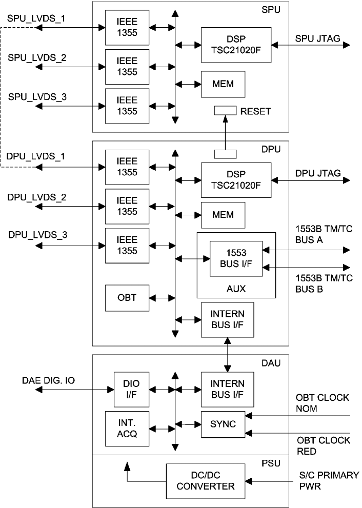
The REBA is composed of three boards, two DSP boards and one board for the DAE interface function and the DC/DC Converter. The DPU Digital Signal Processor (DSP) board is in charge of the control of the different elements: its software controls the DAU board by means of the Internal Bus and it also controls the SPU DSP board by an external spacewire connection. The DC/DC converter supplies all the functions. Table 1 shows the DPU and SPU characteristics and performance.
| Feature | DPU | SPU |
| Program ROM Size | 32 KW x 48 | 32 KW x 48 |
| Program RAM Size | 512 KW x 48 (0 wait state - EDAC protected) | 512 KW x 48 (0 wait state - EDAC protected) |
| Data RAM Size | 512 KW x 32 (0 wait state - EDAC protected) | 512 KW x 32 (0 wait state - EDAC protected) |
| Exp. Data RAM Size | Not implemented | 512 KW x 32 (0 wait state - EDAC protected) |
| EEPROM Size | 256 KW x 48 | Not implemented |
| Interface to MIL BUS | Included in Auxiliary Board | Not implemented |
| OBT timer | PMPSC | PMPSC (Not used) |
| Watchdog timer | DMPSC | DMPSC |
| SMCS Interface | One IF with three LVDS channels | |
| DSP Operation | 18 MHz | |
| Interface to DAU | - End of Acquisition Interrupt - Internal analog acquisitions - 1Hz Interrupt - Converter Sync status input - 1Hz signal control | Not implemented |
| Interface to DAE | - DAE Power Status input - DAE reset SMCS1 output - DAE reset SMCS2 output | - DAE Data ready Interrupt |
| Interface to SPU | - Reset to SPU | - Reset from DPU |
2.1 DSP module
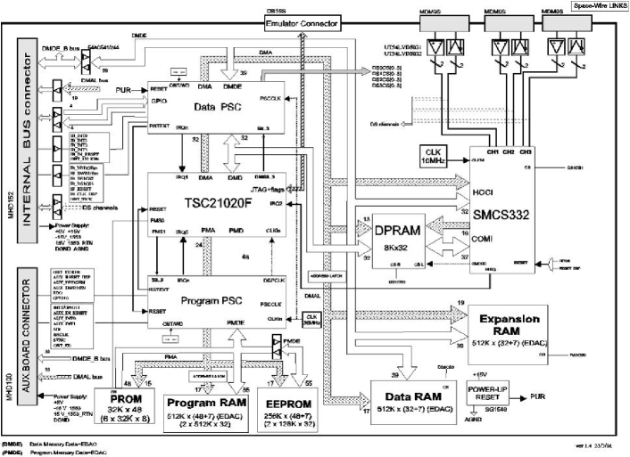
The Processor Module - see block diagram in Figure 4- is a Floating Point Digital Signal Processing CPU on a single board based on the DSP TSC21020F, radiation tolerant version of the ADSP21020 from Analogue Devices. Its external and open Harvard architecture provides two complete bus systems for program (48 bits) and data (32 bits), allowing concurrent access and simultaneous fetching and data accesses or multiple data accesses on a single clock cycle. Expansion capabilities are provided via the backpanel system bus as well as a mezzanine auxiliary interface. The Processor Module implements into a single board: 6x32 Kbytes PROM, 256K x 64 bits EEPROM (EDAC protected), 512K x 56 bits program RAM (EDAC protected) and 512K x 40 bits data RAM (EDAC protected), 512K x 40 bits of Expansion RAM; three high-speed IEEE-1355 (SpaceWire) links, asynchronous serial interface; Expanded interrupt capabilities; System Bus control; Programmable Watch-dog & system Timer and IEEE 1149.1 (JTAG) interface.
General Features: TSC21020F IEEE 32/40 bits Floating Point Digital Signal Processor at up to 18 MHz, 0 wait states for RAM. Harvard architecture with independent program and data memory buses. IEEE 1149.1 I/F (JTAG) for testing and debugging. On-chip emulation. 6x32Kx48bits start-up PROM, 256Kx64bits EEPROM program bank (EDAC protected), 512Kx56 bits Program RAM (EDAC protected) and 512Kx40 bits Data RAM plus an optional 512Kx40 Expansion RAM bank (both banks EDAC protected). 6 Interrupt levels (4 of them through the System Bus) and IEEE Exception Handling with Interrupt on Exception. Bi-directional IEEE-1355 (SpaceWire) based on SMCS332 and LVDS drivers capable of 100 Mbps data rates. Programmable Watch-Dog and 32 bit system Timers. Power and Reset monitor. System Bus Interface (Master). Unit Monitoring and Control capabilities through System Bus. Standard development tools from Analog Devices.
Key Design Features: Performance (at 18 MHz): 18 MIPS, 54 MFLOPS (peak) 36 MFLOPS (sustained). EDAC, UART, Timers, General purpose I/O registers and Glue logic integrated into the Processor Support Chip (PSC) ASIC designed and developed by CRISA. High degree of expansion, compatibility and configurability through the system bus interface and Auxiliary bus interfaces: The System Bus interface has been designed for connecting the DSP to maximise the expansion possibilities (I/O modules, etc.). The Auxiliary bus interface has been designed for connection of a mezzanine auxiliary board originally intended for high speed interfaces such as the 1553/OBDH bus interface, EEPROM/RAM expansion, etc.
The purpose of the PSC Chip is: To enhance the on-chip memory management capabilities of the DSP, providing additional address decoding and wait state generator. Four IO Areas are provided per decoding bank. To provide a flow through EDAC, configurable in width and enabling per I/O Area. To provide a simple 32 bit programmable Timer. To provide a Complex Timer configurable to provide a System Watchdog or an On-Board Time (OBT) support counter-timer. To provide a high speed UART. To provide buffer control in order to support the implementation of extension buses. The design of the PSC is compatible with the use in the PMB and DMB. It considers the bit aligning and bus wideness.
2.2 Auxiliary board
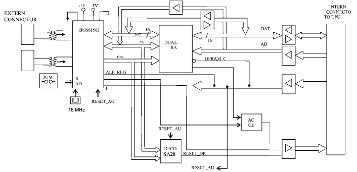
The 1553B Interface function is responsible for the communication between the DPU and the CDMS. As part of the DPU board, this block is implemented on an independent board inserted in the Auxiliary Connector of the DPU board itself. The block diagram of this function is shown in Figure 5. The external connection is of course to the 1553B Data bus. As required by the MIL-STD-1553 standard, the connection is made to both buses, and the implementation is by transformer coupling. The Remote Terminal Address, is discrepant to the standard being internally hardwired, and is different for the Nominal and Redudant Units.
The architecture of the 1553B interface is built around the DDC BU61582. This hardened device provides a completely integrated BC/RT/MT interface between the host processor and the bus, although its use in the REBA is reduced to Remote Terminal mode. It integrates dual transceiver, protocol, memory management and processor interface logic. It also includes internal 16Kwords of RAM which is not used in the design due to its very low speed characteristics.
The interface for data with the DPU software is performed by means of a Dual-Port RAM. The software can also access the internal BU61582 internal registers, and an acknowledge generator is included to allow access even in case the component is processing commands. This circuit also ensures no conflict appears in the accesses to the Dual-Port RAM.
The interface also includes circuitry to generate a general DPU reset on reception of a SA28R command over the bus. The block implements some logic to avoid feedback problems between this reset line, that is sent directly to the DPU, and the general reset line from the DPU that is activated immediately after. It introduces a delay allowing the transmission of the status response through the 1553 bus after the reception of the command.
The interface with the DPU board through the Auxiliary connector also includes a buffering stage which is not part of the DSP board. This stage decouples the internal Aux board operation from the DSP activities. This board uses two secondary voltages supplies: 5V for the general logic as well as for the BU61582 and V, a devoted DC/DC converter output with its corresponding return line. The general logic and DC/DC converter return lines are connected in order to decouple the large peak currents related to the bus communications from the general supply lines.
2.3 DAU function
The DAU is included on the Power Supply Unit (PSU) board together with the DC/DC Converter. The DAU acquires the analogue housekeeping of the REBA performing analogue signal conditioning, digital conversion, and transmission to the DPU via the back panel connector.
Figure 6 shows the DAU functional blocks. The specific DAU functions are: Internal Bus Interface. Analogue to Digital Conversion. Acquisition Control. Clock Divider. Thermistors Conditioning. Secondary Currents Conditioning. Secondary Voltages Conditioning. Internal Test Voltages Conditioning. Status.
The DAU is a slave function controlled by the DPU module. The DPU generates the Bus lines that handle the DAU by means of write and read bus cycles. The "Start of an acquisition cycle" signal is generated with a write command by the DPU. This command enables the Acquisition Control Block and starts a cycle of acquisition. The Status Block contains the following information: “Acquisition in progress” bit, when set, this indicates that an acquisition cycle was started and has not still finished; when cleared, this indicates that an acquisition cycle finished and a new cycle can be started. FIFO Flags: Three bits that indicate the FIFO status (empty, not empty, full, etc.). OBT clock status which indictes if the REBA OBT counter is using the external or internal clock.
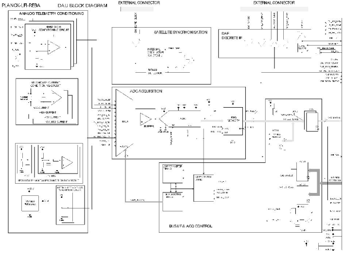
In the Analogue to Digital conversion block the analogue signals are routed to a 16 channel multiplexer stage of type HI-546. The selected signal is buffered by an OP-42 Operational Amplifier and applied to the input of an Analogue to Digital Converter (ADC) type AD-574. The 9 most significant bits output of the ADC are stored in a FIFO memory. The method of acquisition is cyclic. Once all the channels have been sampled and placed in the FIFO the Acquisition in Progress signal is deactivated so that the DPU can read out the data.
The RS-422 block of the DAU provides the interface to the DAE for the 1 Hz time synchronisation signal used by the DAE at power up and during the process of time synchronisation with the OBT. The signal is derived from the 2 Hz signal generated by the CPU. Its phase is controlled (by DPU software and by means of two signals) in order to ensure a rising edge when required, both at power up and during the synchronization procedure. Three temperature monitoring telemetries are provided by the DAU function: the DPU board temperature, the SPU board temperature and the PSU board temperature, using NTC type thermistor. Four secondary voltage monitoring telemetries are provided by the DAU function: the VCC voltage (logic supply), the V voltage (positive analogue supply) and the V voltage (negative analogue supply), and the V_1553 voltage. The currents of these secondary voltages, sensed at the active path of the secondary, are also provided. Each conditioning circuitry includes a filter with Hz.
2.4 DC/DC Converter
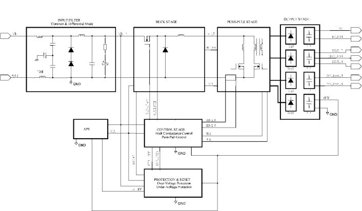
Figure 7 is a block diagram of the DC/DC Converter which uses the buck fed topology commonly used in space programs. The converter operation starts once the power bus is present at the input. There is no command to turn On or Off the converter. The “Buck stage” provides the voltage regulation at the output while the “push-pull stage” transforms the voltage to the output levels. The converter has both common mode and differential mode filters to reduce the emissions onto the main bus as shown in the block diagram.
Once the PDUt power bus is available, the converter turns On in a smooth manner because the inrush current is limited by means of an external latching current limiter in the PDU to avoid the peak current due to the charging of the differential filter. Once the input filter is fully charged the converter starts operating. This is achieved by means of an under-voltage detector that does not allow the operation of the converter until the filter is completely charged. This is necessary to guarantee that the converter control electronics is supplied at the correct voltage and that the converter starts in a well known and safe mode. The DC/DC converter incorporates over-voltage protection. Over-current protection is implemented on the primary side by means of the buck stage in case of a short circuit or overload on the secondary side.
2.5 Grounding concept
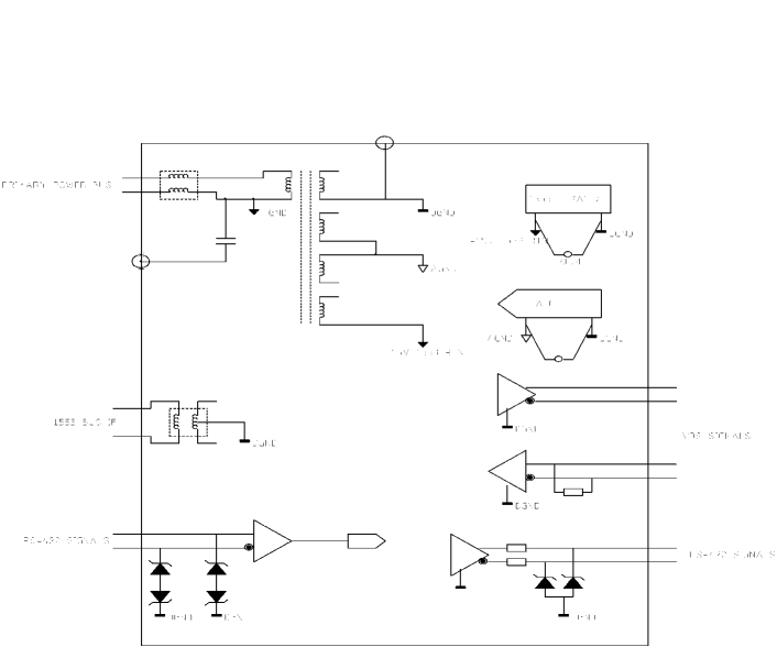
The grounding of the REBA is via a single secondary return star point connected to equipment chassis in a single point. Primary return is isolated from chassis and from this secondary common return. Detailed grounding diagrams are shown in Figure 8. The different boards, including the mother board, include ground planes for the different secondary returns.
2.6 Redundancy
The whole of LFI was analysed during the early design phase for the effects of failures, and a redundancy approach was adopted to reduce the possibility of single point failures causing total loss of the instrument. As the REBA itself would inherently be a point of single point failure unless very complicated internal redundancy solutions were adopted that would themselves tend to compromise the overall reliability of the unit, a simple approach was adopted of replicating the unit for use in cold redundancy and thus also implementing cold redundant interfaces to both the service module of the spacecraft (which themselves were further redundant at the individual unit level) and the rest of the instrument. In addition the failure analysis of the REBA itself was used to make internal design choices and thus where reasonable mitigate single point failures. For example margins were applied to the processor memories to allow for the loss of single memory chips over the life of the unit in orbit. All component choices in the REBA were tightly controlled by the Planck Product Assurance Program under the product assurance rules of ESA and also burn-in and ESA derating requirements were applied to limit the possibility of the most likely cause of unit failure which would be in single components.
3 Mechanical and thermal design description
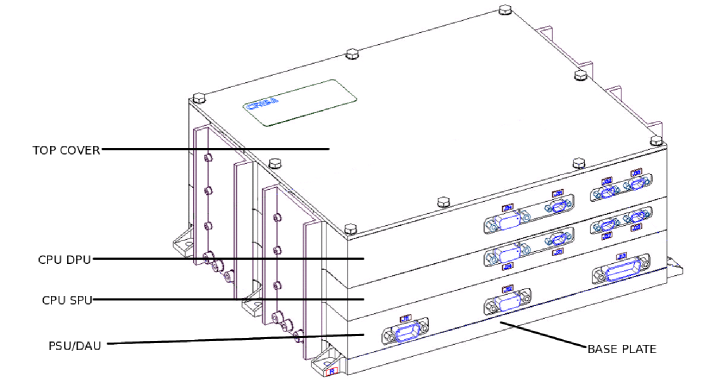
The REBA is an assembly of three modules plus base plate with motherboard and a top cover, distributed as is shown in Figure 9. In addition to these modules the REBA has one independent motherboard, called the auxiliary board.
The principal objective of the thermal design was to avoid hot spots and high thermal gradients between the different parts of the unit. The PCB’s are coated with varnish to ensure good radiative coupling between boards and this also contributes to the homogeneity of board temperatures. The PCB design includes thick copper planes and the preferred location on stiffener and/or wide copper tracks of components with high power dissipation. Externally, the box parts are painted in mat black with an emissivity of 0.9.
The housing concept is an assembly of machined parts assembled by screws. The housing modules are mounted horizontally, stacked one on the top of the other. The REBA has two identical CPU boards, DPU (Data Processing Unit) and SPU (Signal Processing Unit), with some differences in terms of size of memory banks and external interfaces. The DPU Module has a higher stiffener than the SPU Module because it houses the auxiliary PCB.
The I/O connectors and layout of the modules have been optimised in order to minimise the height of the box. MHD connectors serve as interfaces for electrical interconnections between modules through the motherboards.
The Base Plate is a machined plate having a flat contact surface to the platform. This item has a pattern of mounting feet, total 6 (M4), located along the housing perimeter and machined from a single block providing a continuous flat bottom surface. The Top Cover is a 2 mm thick aluminium sheet. The modules that form also the sides of the boxes have lateral reinforcements to provide stiffness and thermal conductive coupling between the modules and the base plate. The boxes are assembled by means of screws, passing through the Top Cover and through the stiffeners to the base plate threaded inserts. The items of the housing are machined parts made of aluminium alloy, having through holes or threaded inserts along their edges to allow easy assembly, minimising the number of mechanical parts. Figures 10, 11, 12 and 13 show a view of the modules.
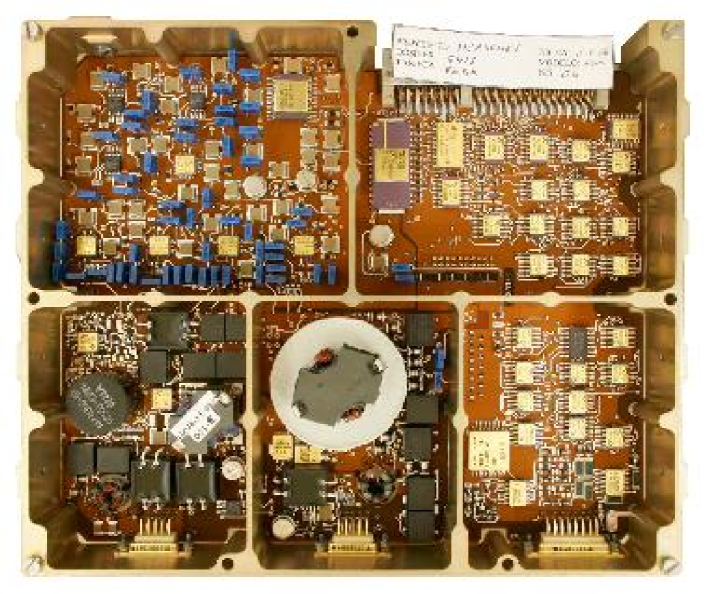
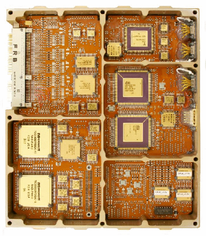
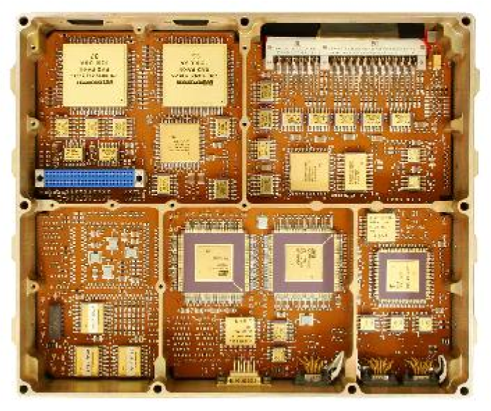
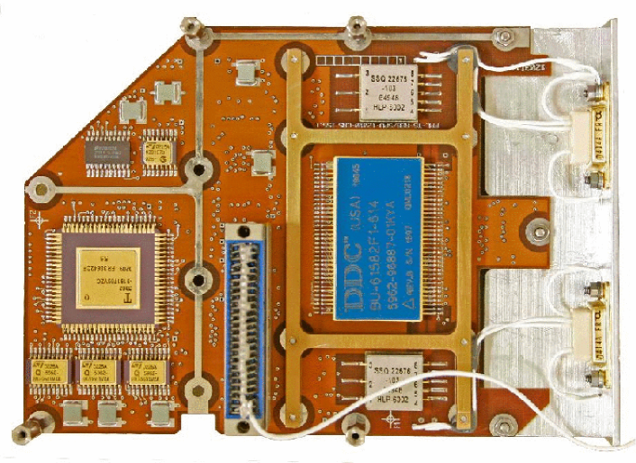
The PCB is used for mounting components as well as printing wiring interconnections between components. The components selected are surface mounted (SMT) whenever possible to minimise mass and volume. The components were selected for insertion mounting where high thermal dissipation was necessary through the stiffeners or the SMT versions were not available. The PCB is made of a resin polyimide and fibreglass multilayer laminate. The required surface to allocate the electronic components is optimised in order to have a minimum number of internal connections.
The stiffener frames have several functions: To provide adequate stiffness to achieve natural frequencies on board above 140 Hz. This is achieved by machining them from a block of aluminium alloy with contours along the edges of the boards, and inner ribs dividing the PCB areas in to smaller unsupported sections. To provide PCB fixation by means of M2.5 screws in a sufficient number to guarantee structural redundancy and thermal conductive coupling. To serve as heat sinks for high dissipation components, such as power mosfets. To provide fixation for the I/O D*M and MDM connectors located on the front of the units. Internal interconnections between modules is performed by a motherboard using Medium High Density (MHD) connectors. The material used for the mechanical parts of the box is aluminium 6082-T6 and its surface treatment is chromate and Black paint.
4 Design, development and AIV
The following models were manufactured and tested at various levels. Two identical engineering models: EM and AVM, the engineering qualification model: EQM and the flight model: FM (both Nominal and Redundant). The REBA EM and AVM models are flight model representative of both the electronic circuitry interfacing the S/C and support the LFI flight software. Commercial electronic parts were used with the same technology and by the same manufacture for the circuits directly interfacing with the S/C subsystem as in the flight H/W. The REBA-EQM is representative of the FM with the following exception: the EQM electronic components are "extended range" type only; nevertheless, they have been procured from the same supplier as that of the FM components and have been produced with the same FM technology. The REBA-FM has full flight standard components and was verified by formal functional and environmental acceptance tests. In order to save costs flight spares (FS) boards have been produced for replacement of failed or damaged equipment at the integration or launch sites if it had been necessary.
The development of the REBA was split into four main phases: Preliminary Design Phase, Detailed Design Phase, Flight Design Qualification Phase and Flight Acceptance Phase. During the Preliminary and Detailed design Phases the equipment concept was confirmed, the interfaces were defined, and the requirements and the design were frozen. The Preliminary and Critical Design Reviews were also held. The EM and AVM model were produced during this stage. During the qualification Phase the flight baseline design configuration, the preparation of the plans and procedures for QM and FM testing, and the manufacturing, assembly, integration and qualification tests of the REBA QM were performed. This Phase was completed with the Qualification Review. The Flight Acceptance Phase was devoted to the manufacturing, assembly, integration and testing of the REBA, nominal and redundant, flight equipment. The production of these models concluded with the corresponding Flight Delivery Review to allow integration of the REBA in the flight model of LFI.
Full self-procurement was established for the EEE parts for the EM and AVM. Components for the EQM and FMs were procured by a Central Parts Procurement Agency provided by ESA. Other specific components and materials such as ASICS, magnetic components, mechanical parts, etc., were procured by CRISA. All the assembly activities of electronic modules including equipment integration were performed by CRISA. A dedicated Product Assurance Plan was prepared to cover the quality assurance aspects related to the engineering, procurement, manufacturing and verification activities involved in the development of the flight models.
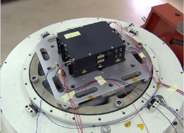
The overall verification program consisted of two parts, the qualification program and the acceptance program. Qualification tests are performed on the EQM model, and acceptance tests on the FM model. The different models were submitted to test in order to verify their characteristics and behaviour in the following areas: physical, electrical, functional, mechanical, thermal vacuum and EMC. Table 2 provides a review of these tests performed on the qualification and flight models in a test matrix form.
| Test | QM | FM |
|---|---|---|
| Inspection Tests | T | T |
| Dimensions, mass, flatness & Roughness | T | T |
| Centre of Gravity, Moment of Inertia | T | T |
| Grounding, Electrical and Functional | T | T |
| Shock Load Test | Q | |
| Sine Vibration | Q | A |
| Random Vibration | Q | A |
| Thermal Vacuum | Q | A |
| Conducted Emissions and Susceptibility | T | T |
| Radiated Emissions and Susceptibility | T | R |
| ESD | T |
5 REBA On-board software overview
All the software of the LFI instrument is implemented in the Radiometric Electronic Box Assembly (REBA). The LFI On-board software is divided into the following software products:
-
•
REBA DPU Start-Up Software: Developed by CRISA. It performs the initialization of the DPU and allows the upload into memory of the DPU Application Software (DPU_ASW) which is stored in the DPU EEPROM. It also performs some hardware self tests to confirm the correct status of the unit.
-
•
REBA SPU Start-Up Software: Developed by CRISA. It performs the initialization of the SPU and allows the upload into memory of the SPU Application Software (SPU_ASW) which is stored in the DPU EEPROM. It also performs some hardware self tests to confirm the correct estate of the unit.
-
•
REBA Low Level Software Drivers: Developed by CRISA. These provide a set of functions which allows the application software to access the different parts of the hardware.
-
•
REBA Application Software: Developed by IAC. It performs the complete operation of the LFI instrument. It is split in two applications running in the two CPU’s inside the REBA, namely, DPU application Software (DPU_ASW) and SPU application Software (SPU_ASW).
-
•
Compressor and Decompressor Software: Developed by IAC, the compressor is implemented as a function of the SPU_ASW. Its development was performed as a separate product and then, integrated in to the SPU_ASW.
5.1 REBA Low-level Software
The REBA low level software consists of the Start-up Software (SUSW) and the Low-Level software drivers (LLSW_DRV). The DPU and SPU SUSW perform the necessary functions to boot the unit at power up, perform a health self-test and start the ASW giving it the control. Both programs are stored and executed from the DPU and SPU PROMs.
The DPU SUSW is in charge of performing the following tasks: Power up initialization. Reset source discrimination. Hardware self-tests. Hardware initialization/configuration. Perform command reception/execution loop, receiving commands and sending responses through the 1553 interface. Transfer control to ASW, upon reception of appropriate command. The SPU SUSW is in charge of performing the following tasks: Power up initialization. Reset source discrimination. Hardware self-tests. Hardware initialization/configuration. Perform command reception/execution loop, receiving commands and sending responses through the 1355 interface. Transfer control to ASW, upon reception of appropriate command.
The Low-Level software drivers (LLSW_DRV) package is a set of primitives (source/object code) that provide easier access to functionalities of the different DPU/SPU HW devices which are compiled/linked with the ASW. The LLSW_DRV includes the following drivers: MILSTD 1553 (ACE device). Watchdog. OBT. Data Acquisition Unit. SMCS 1355. Interrupts. EDAC. EEPROM. General definitions. Error codes. Hardware map. DSP 21020 driver. PSC driver. Software reset function. Memory management. Both, LLSW_DRV and SUSW are coded in C and Assembler languages and are implemented using the Analogue Devices Software Development Environment ADSP-21020 Family Development Tools, release 3.3 for PC. The Architectural design was performed using HOOD/UML tools. Software requirements verification was carried out by test, analysis or assessment (review of the design). Unit testing was performed using the ATTOL unit tests tool and for the software integration the Analogue Devices DSP 21020 Emulator. SUSW and LLSW_DRV software packages have been developed according to Planck LFI REBA/Herschel PACS SPU SW Quality Assurance Plan and comply with the CRISA SW Configuration Management Plan.
5.2 REBA Application Software
5.2.1 Functionalities
The Data Flow Diagram in Figure 15 shows the main functions performed by the REBA_ASW. The CDMS communication component is in charge of packing and transferring all data produced in the instrument (Telemetry): science data reduced and compressed (sc_drc), housekeeping packets of the whole instrument (hk_pcks), events and execution reports (exec_reports), according to CDMS protocols (high and lower levels). This component also receives and decodes every TC received from the CDMS according also to CDMS protocols (high and lower levels) to produce valid instrument commands ready to be executed, immediately (valid imm TC) or waiting in an execution queue for eventual previous TCs execution (valid TC).
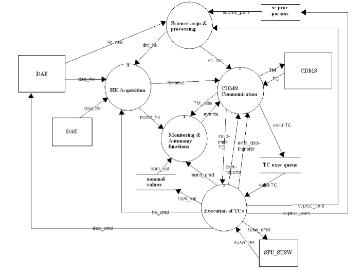
The main function of the REBA_ASW is to receive from the Data Acquisition Electronics (DAE) the raw science data (Sc_raw) collected by the LFI radiometers and reduce and compress these data (Sc_drc) to within the allocated bandwidth allowed to the instrument. The baseline for the science data processing is to average, perform differences and compress the data of all the detectors, nevertheless, the type of processing as well as the selection of the detectors to be processed is modifiable by TC (scproc_cmd). Some parameters needed for the science processing can also be modified by TC (scproc_pars).
The REBA_ASW also collects housekeeping from the whole instrument. These data are collected from the Data Acquisition Unit (DAU) inside the REBA (dau_hk), which supplies information on the REBA itself, and from the DAE (dae_hk) which supplies information about the rest of LFI instrument. Other housekeeping is produced by the REBA_ASW itself, as is the case for the processing of the science data (drc_hk) as well as other parameters (not included in the diagram for simplicity). This function is performed by the HK acquisition component. The operator may also require by TC (hk_cmd) special HK information for diagnostics and debugging purposes. The housekeeping collected are sent to the CDMS as specific types of TM packets (hk_pcks) and some of these are also checked by the REBA_ASW to control the health of the instrument (monit_hk).
This automatic checking is performed by the “Monitoring & Autonomy functions component”, which takes care of the CPU load in the SPU, temperature of the focal plane; science TM rate and instrument internal communications links. When the chosen values exceed certain nominal values (nom_val), an alarm is sent to the CDMS (events) and an autonomy function is activated to maintain the system in safe conditions. It is also possible to command (monit_cmd) this component for testing and debugging purposes.
Finally, the other main component of the REBA_ASW is the management of the TCs received from the CDMS, Execution of TCs component. It controls the correct execution of the incoming TCs (valid_TC and valid_imm_TC) which operate the instrument. It only allows the execution of TCs under certain conditions of the system. It sends the TC to the appropriate subsystem or component when needed, checks the completion execution and notifies the CDMS about the results (exec_reports). The transmission of TM packets to the CDMS may also be modified by TC (enbl_dsbl_transfer) for testing and debugging purposes allowing the enabling and disabling of the transmission of different telemetry packets.
5.2.2 Architecture
The REBA_ASW is composed of two applications programs running on the two CPU’s of REBA, DPU application software (DPU_ASW) and SPU applications software (SPU_ASW), respectively.
Both applications were developed in C language and are executed under the real time operating system Virtuoso, from Eonic Systems. Some specific functions, critical in time, have been implemented in assembler.
To cope with the functionalities described in the previous paragraph, REBA_ASW has been built by the use of different Virtuoso objects. It is composed of a set of Virtuoso tasks which interface among them by the use of some Virtuoso Fifos, memory maps as well as global variables. Problems of racing and concurrency have been solved by an appropriate definition of a priority scheme of tasks as well as the use of Virtuoso semaphores and resources. Virtuoso timers have also been used to implement some cyclic activities. In Appendix B, we list and describe the most important tasks of the REBA_ASW.
5.2.3 Verification and Validation
A total of 91 test procedures were defined and executed to ensure that the REBA_ASW fulfils its software requirements. The validation was performed against the Software Specification Document, [4]. Validation is completely defined in [6].
The acceptance tests consist of a set of validation procedures in a specific order. These acceptance tests have been executed for each REBA hardware model.
Unit tests have been executed at function level to check that each function executes according to its detailed design. Different tests cases for each function have been executed to guarantee a 100% statement coverage. More details about unit tests can be found in [3].
5.2.4 Metrics
Table 3 provides metrics which indicate the maturity of the REBA_ASW.
| Source Modules | C functions | Assembler functions | Code lines | Comment lines | Nesting Max | McCabe | |
|---|---|---|---|---|---|---|---|
| DPU_ASW | 41 | 264 | 4 | 10100 | 14091 | 2.53 | 5.44 |
| SPU_ASW | 36 | 139 | 3 | 4679 | 7341 | 2.09 | 4.13 |
| Compressor | 2 | 10 | 0 | 224 | 1.4 | 3.7 | |
| Decompressor | 2 | 9 | 0 | 242 | 2.22 | 5.22 |
6 The SPU Compressor Module
6.1 Compressor requirements
The LFI scientific mission requires compressing the scientific data in order to make maximum use of the satellite to ground communication bandwidth. IAC developed the compressor function which has been integrated in the SPU application software. A decompression function was also developed and delivered to the Data Processing Center (DPC) in order to be integrated in to the ground application software.
The SPU compressor component is particularly complex and, therefore, a complete set of formal software documentation has been generated and delivered specifically for both compressor and decompressor functions, consisting of a software specification document ([13]), which includes SW requirements and architecture design, a software verification and validation plan document ([12]) and its corresponding validation plan report ([11]), and a unit test plan and unit test report documents.
The compressor input signal is expected to be dominated by white gaussian noise, with information content or entropy for 30 GHz channels of bits, which allows for a maximum compression ratio of , and the specified minimum compression ratio for such a signal is about . In addition, the compressor is required to be lossless and adaptive, which means recovering the exact input signal after decompression, and optimizing compression performance in spite of variations in the input signal statistics, respectively. All these requirements, together with the common requirements of on board compressors of working in real time and packetizing output data in independently decompressable packets, has led us to a careful selection of the compression algorithm, and a great deal of work to adapt it to the LFI compressor requirements.
Arithmetic coding is the method of choice for lossless adaptive entropy compression on multisymbol alphabets because of its high speed, low storage requirements and effectiveness of compression. The final SPU compressor is an adaptation of the implementation of the arithmetic coder by A. Moffat, a widely used non commercial version which has become a standard ([9]).
6.2 Compressor general architecture
Adaptation of Moffats algorithm to LFI requirements has been viable thanks to its modular architecture. Figure 16 shows the modular architecture of the SPU compression function ([14]). This function is called by the SPU application SW with the aim of generating a single compressed data set for a single science TM packet. Each time the function is called, all the relevant compression variables are set to the same initial values.
The coding module is the core of the compression function, and those options that maximize the compression factor without penalizing execution speed have been chosen. For example, multiplications and divisions are allowed, because they are supported by the DSP as primitive operations, and permit a better compression efficiency; and frugal bits mode is selected, so that coding termination is made with as few nonambiguating bits as possible.
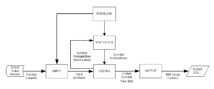
The modelling module informs the rest of the modules about the nature and characteristics of the signal. The model is a 16 bit integer zero order adaptive model, which means that 16 bits uncorrelated input samples are assumed, with an unknown initial statistic.
The statistics module manages the Fenwick Tree structure that stores the symbols cumulative frequencies. Accessing the structure takes instructions per symbol, where is the size of the alphabet, and so the cost is small even when is very large (which is our case with symbols). Initially, the symbols occurrence frequencies are set to zero. In order to code a symbol with a zero occurrence frequency, an escape symbol is coded followed by the raw symbol. This allows a fast initialization that would otherwise prevent real time operation. This also allows the statistics table to truly represent the signal statistics right from the beginning of the compression operation with as little increment in a symbol occurrence frequency as unity per new symbol, so that no time consuming functions are needed to read just the statistics table because of overflow.
Input and output modules read the input data and write the output data according to the interface requirements with the SPU application software. The output modules take care that the maximum allowed size of a compressed data set per TM packet is not exceeded.
6.3 Performance validation and results
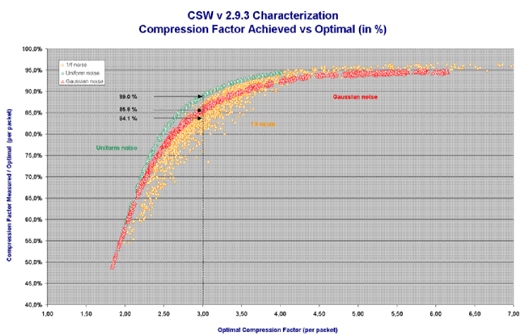
A formal SW validation has been conducted (see [11] and [12]) against the compressor SW requirements specified in [13]. Concerning performance on compression ratio and execution time the developed compressor is compliant. For a Gaussian white noise signal with an optimal compression ratio of around , the minimum achieved ratio is , and the maximum execution time per generated packet is 46 ms.
Also the compressor ratio has been characterised against noise with different probability density functions (see [10]). Figure 17 shows the percentage of achieved compression ratio versus the optimal, for Gaussian, uniform and types of noises. We can see that the compressor behaves slightly better for uniform noise than for the other two types. This is because a uniform probability distribution is more robust against roundoff error due to integer arithmetic divisions when calculating the symbol’s probabilities. However, for a Gaussian noise, which is the most representative of the actual expected scientific input signal, the achieved compression ratio is specification compliant.
7 Conclusions
The Radiometer Electronics Box Assembly (REBA) is the control and data processing on board computer of the Low Frequency Instrument (LFI) of the Planck mission (ESA), consisting in two separate identical units, which operate in cold redundancy under power supply control of the Planck spacecraft. Each REBA unit is connected to the instrument DAE and to the spacecraft CDMU and PCDU. REBA performs, among other functions, on-board command and data handling, science data processing and compression, software storage and processing, and control of the LFI. It has four functional units: DPU, SPU, DAU and PSU. It is composed of two DSP boards and one board for the DAE interface function and the DC/DC Converter.
We have manufactured and tested at various levels engineering models (EM and AVM), the engineering qualification model EQM and the flight model FM (both nominal and redundant). Specific software was developed to carry out the start-up of the DPU and SPU, to perform the complete operation of the LFI instrument, and to carry out on-board data compression in order to make maximum use of the satellite to ground communication bandwidth. The compressor function was integrated in the SPU application software. The performance on compression ratio and execution time was found in agreement with the specifications.
After launch of the Planck satellite on May 14th 2009, the REBA hardware and software performs well and fulfil successfully all the specifications for flight operations.
Acknowledgements.
Planck is a project of the European Space Agency with instruments funded by ESA member states, and with special contributions from Denmark and NASA (USA). The Planck-LFI project is developed by an International Consortium lead by Italy and involving Canada, Finland, Germany, Norway, Spain, Switzerland, UK, USA. The development of REBA has been funded by the Spanish Ministry of Science through the National I+D+i Plan with several research grants awarded in the period 1998-2008. We would like to acknowledge the very significant contribution of the company CRISA to this project. We also thank INTA for providing access to their facilities. We are indebted to the IAC technical, scientific and administrative staff for their support. The authors also wish to acknowledge the funding by ASI to the Italian LFI Program.References
- [1] Bersanelli et al. 2009, A&A Submitted.
- [2] Gómez Reñasco, M. F. & Obradó Girona, A. 2004, LFI-REBA Application Software Specification. PART B: Architectural Design. DS/SR-FIR/093v.3. Issue 3. June 24, 2004.
- [3] Gómez Reñasco, M. F. 2007, LFI-REBA APPLICATION SOFTWARE UNIT TESTS REPORT. DS/SR-FIR/289v.14. Issue 4. April 14, 2007
- [4] Gómez Reñasco, M. F. 2007, LFI-REBA Application Software Specification. PART A: Software Requirements. DS/SR-FIR/062v.5. Issue 5. April 30, 2007.
- [5] Gómez Reñasco, M. F. 2007, LFI-REBA Application Software Specification. PART C:Telecommands And Telemetry List. DS/SR-FIR/075v.5. Issue 5. April 30, 2007.
- [6] Gómez Reñasco, M. F. & Obradó Girona, A. 2007, LFI-REBA APPLICATION SW VERIFICATION AND VALIDATION TEST PLAN AND PROCEDURES (SVVP/VT). DS/SR-FIR/129v.14. Issue 14. April 05, 2007
- [7] Lamarre et al. 2009, A&A Submitted.
- [8] Mandolesi et al. 2009, A&A Submitted.
- [9] Moffat, A., Neal, R. M., Witten, I. H. 1998, Arithmetic Coding Revisited, ACM Transactions on Information Systems, volume 16, number 3, July 1998, pp. 256-294
- [10] Sánchez, M. 2005, Characterization of the LFI on board CSW_REBA version 2.9.3. IAC code: DS/TN-FIR/231v.1 Issue 1. June 7, 2005.
- [11] Sánchez, M. 2005, LFI CSW and DCSW Software Verification and Validation Test Report. IAC code: DS/PR-FIR/205v.3 Issue 3. June 9, 2005
- [12] Sánchez, M. 2005, LFI CSW and DCSW Software Verification and Validation Plan/Validation Test Plan and Procedures (SVVP/VT. IAC code: DS/IV-FIR/201v.2 Issue 2. June 13, 2005
- [13] Sánchez, M. & Chulani, H. 2005, LFI Compressor and Decompressor Software Specification Document. IAC code: DS/SR-FIR/141v.2 Issue 2. August 16, 2005
- [14] Sánchez, M. & Chulani, H. 2005, LFI CSW and DCSW Algorithm Description. IAC code: DS/TN-FIR/293v.1 Issue 1. October 25, 2005
Appendix A Abbreviations and acronyms
| ASIC | Application Specific Integrated Component |
| ASW | Application Software |
| AVM | Avionic Model |
| CDMS | Central Data Management System |
| CDMU | Central Data Management Unit |
| DAE | Data acquisition Electronics |
| DAU | Data Acquisition Unit |
| DMB | Data Memory bus |
| DMPSC | Data Memory Processor Support Chip |
| DPU | Data Processing Unit |
| DSP | Digital Signal Processor |
| EDAC | Error Detection and Correction |
| EQM | Engineering Qualification Model |
| ESA | European Space Agency |
| ESD | Electro Static Discharge |
| FIFO | First-In First-Out |
| FM | Flight Model |
| FS | Flight Spare |
| Gxxxx | 230 xxxx |
| HW | Hardware |
| IO | Input/Output |
| Kxxxx | 210 xxxx |
| LFI | Low Frequency Instrument |
| LLSW | Low Level Software |
| LLSW_DRV | Low Level Software Drivers |
| Mxxxx | 220 xxxx |
| PCDU | Power Control Distribution Unit |
| PCB | Printed Circuit Board |
| PMB | Program Memory Bus |
| PMPSC | Program Memory Processor Support Chip |
| PROM | Programmable Read-Only Memory |
| PSC | Processor Support Chip |
| PSU | Power Supply Unit |
| RAA | Radiometer Array Assembly |
| RAM | Random Access Memory |
| REBA | Radiometer Electronics Box Assembly |
| ROM | Read-Only Memory |
| S/C | Spacecraft |
| SMCS | Scalable Multichannel Communication Subsystem |
| SPU | Signal Processing Unit |
| SUSW | Start Up Software |
| SVM | Service Module |
| SW | Software |
| TC | Telecommand |
| TM | Telemetry |
Appendix B DPU_ASW and SPW_ASW architectures
| Task | Description | Priority |
|---|---|---|
| tDpuInit | This task is the execution entry point of the complete application. It initializes all variables and Virtuoso objects (semaphores, timers, etc.) and starts the rest of tasks. After this initialization it aborts its own execution. | 8 |
| tCdmsDrv | Implements the transfer layer protocol to communicate with the CDMS. This communication is based on an interrupt handler which is executed at reception of two types of interruptions produced by the 1553 interface, that is, one interruption at subframe level (1/64 seconds) and the second one at frame level every second. The interruption at frame level is also used to perform the synchronization of the REBA with the spacecraft time. It manages TCs received by validating the TC received and executing those of immediate type and storing in a FIFO and a memory map those which are queue TCs. These later are processed by tTcExecution task. This task also interfaces with TM rate monitoring task by storing in a global variable the total of delivered science TM packets. | 10 |
| tDpuDmpscDrv | This task manages events and errors produced by the Processor Support Chip (PSC) of Data Memory of SPU. These events are detected by interruption. This includes the management of EDAC single and double failures in data memory, watchdog and hardware errors on the 1553 interface. Single EDAC failures are also corrected by this task. | 16 |
| tDpuPmpscDrv | This task manages events and errors produced by the Processor Support Chip (PSC) of Program Memory of DPU. These events are detected by interruption. This includes the management of EDAC single and double failures in program memory as well as the 1 Hz signal which is used to perform the synchronization of DAE. | 17 |
| [h!] tDpuSmcsDrv | This task implements the low level communications of the 3 links of the 1355 interface. Link 1 is used for communications between DPU and SPU and link2 and link3 is used to communicate DPU with DAE. While link 3 is used for transmission of data between DPU and DAE, link 2 implements the called "control by link", that is, as DAE has no software, the operation of the DAE SMCS chip must be commanded through a link, so, DPU commands DAE SMCS to perform the appropriate transmission and receptions through this link. Depending on the information of the interruption, this task signals appropriate semaphores or set values in a FIFO; these Virtuoso objects are then used to communicate to other higher level tasks of communications. | 18 |
|---|---|---|
| tDpuRcvFromSpu | This task processes the different packets received from the SPU, the discrimination of the reception is based on a FIFO. The reception is performed in a double buffer in such way that while a packet is being processed another one can be received. According to the type of packet it performs different activities, such as, saving SPU HK information for further packing of REBA HK packet; obtaining science diagnostics data for further science diagnostic statistics generation; storing in a FIFO the SPU CPU load for monitoring, etc. | 25 |
| tRebaHkAcq | Based on a 1 second timer, it collects nominal as well as diagnostic acquisition data for REBA HK packet. The complete diagnostic data are collected for each sample period and, depending on the transmission enabled of TM packets, this is sent or reduced to just send the nominal values, a smaller packet. | 30 |
| tDaeHkAcq | Based on a 1 second timer, it collects and packs the 2 types of DAE HK data, that is, fast HK (every 1 second) and slow HK (every 64 seconds). It also selects and stores in a FIFO the Focal plane temperature (Fpt) values for further monitoring analysis. | 31 |
| tFptMonit | Implements the monitoring of the Focal Plane by checking the values stored in a FIFO. After comparison with a threshold value it also sends an event report and executes an autonomous function which commands DAE to switch off the 4 DC/DC converters of the Front End Unit. | 35 |
| [h!] tCpuMonit | Implements the monitoring of the SPU CPU load by checking the values stored in a FIFO. When limit is exceeded it sends an event report. | 36 |
|---|---|---|
| tTmrMonit | Based on a timer, whose period is configurable by the user, the total of science TM delivered is checked. When the TM rate exceeds the expected values an autonomous function to disable the processing in some detectors is executed. The disabling is based on a table which can be configured by the user. | 38 |
| tDpuEventMngr | All errors produced in the DPU system are managed by this task. It processes all errors from a FIFO which is filled by all tasks when errors are produced. This task also distinguishes when the error must be sent as event reports. | 40 |
| tTcExecution | Obtain from a FIFO the queued TCs pending of execution. These TCs are already validated. The FIFO contains the storing information referred to a memory map where the complete TCs are stored. Once the TC is executed, it sends the corresponding execution report, success or failure. Synchronization of both REBA and DAE is performed by the coordination of this task with tCdmsDrv and tDpuPmpscDrv tasks. See later. | 45 |
| tDpuMemoryScrub | Based on a 24 hours timer, it reads all memories of DPU. This allows to correct eventual single EDAC errors, decreasing, on this way, the risk of double EDAC failures. | 60 |
An important aspect to mention of the tTcExecution task is the synchronization of REBA and DAE to the spacecraft time. REBA synchronization is carried out by the use of global variable and a semaphore. TcExecution task set a flag to indicate the synchronization process to tCdmsDrv task. When this flag is asserted tCdmsDrv uses the one second interruption of 1553 interface to set the REBA OBT according to the time received, a semaphore indicates to the tTcExecution task that the synchronization has finished. A similar process to verify the REBA time is followed. DAE synchronization process is similar; in this case, tDpuPmpscDrv task guarantees that the synchronized time is passed to DAE in advance to a 1 Hz interruption which is used by DAE to latch its time.
| Task | Description | Priority |
|---|---|---|
| tSpuInit | This task is the execution entry point of the complete application. It initializes all variables and Virtuoso objects (semaphores, timers, etc.) and starts the rest of tasks. After this initialization it aborts its own execution. | 8 |
| tSpuDmpscDrv | This task manages events and errors produced by the Processor Support Chip (PSC) of Data Memory of SPU. These events are detected by interruption. This includes the management of EDAC single and double failures in data memory, watchdog and the Data Ready signal coming from DAE which indicates that a new set of science data has been stored in DAE DPRAM and it is ready for being transferred to SPU. This is done by asserting a semaphore. | 16 |
| tSpuPmpscDrv | This task manages events and errors produced by the Processor Support Chip (PSC) of Program Memory of SPU. These events are detected by interruption. This includes the management of EDAC single and double failures in program memory. | 17 |
| tSpuSmcsDrv | This task implements the low level communications of the 3 links of the 1355 interface. Link 1 is used for communications between SPU and DPU and link2 and link3 is used to communicate SPU with DAE. While link 3 is used for transmission of science data from DAE to SPU, link 2 implements the called "control by link", that is, as DAE has no software, the operation of the DAE SMCS chip must be commanded through a link, so, SPU commands DAE SMCS to perform the appropriate transmission through this link. Commands received from DPU are stored in a FIFO which is processed later by the tCmdExec task. The communications with DAE are managed by two semaphores. | 18 |
| [h!] tInitialScProc | This task starts its activity based on a semaphore which is signaled when Data Ready signal, asserted by DAE, is detected. Performs initial processing of science data including data acquisition from the DAE, data validation, and depending on the processing type(s): data summing, differencing, re-quantisation and offset. Data are stored in circular buffers implemented by a Virtuoso memory map. It organize the science data separating by detectors and, depending on the processing type, it stores raw data in circular buffers or performs the sum of the data before store it. Communicates that a science packet is ready to be compressed and/or packaged through a FIFO. | 25 |
|---|---|---|
| tSpuHkGen | Based on a 1 second timer, it collects SPU HK data and transmit this data as a packet to DPU. | 30 |
| tSpuEventMngr | All errors produced in the SPU system are managed by this task. It processes all errors from a FIFO which is filled by all tasks when errors are produced. This task also distinguishes when the error must be sent as event reports. | 40 |
| tScTxToDpu | Transmits a Science SPU packet to the DPU. These packets have been previously stored in SPU DPRAM. A FIFO with memory addresses of Sc packets is the interface with tFinalScProc task. | 43 |
| tCmdExec | It listens from link1 commands received from DPU and executes the corresponding command. | 45 |
| tFinalScProc | Performs final processing of science data, including data compression (depending on the processing type). It obtains packets ready to be compressed and/or packaged. It interfaces with tInitialScProc through a FIFO. TM packet is generated in a dedicated double buffer in the SPU DPRAM, this double buffer allows to transmit a packet while new packet is being produced. | 50 |
| tClbSwitch | Based on timer of 15 minutes, it enables each cycle a detector in sum data processing type in one of 2 provided simultaneous processing groups. | 58 |
| tSpuMemoryScrub | Based on a 24 hours timer, it reads all memories of DPU. This allows to correct eventual single EDAC errors, decreasing, on this way, the risk of double EDAC failures. | 60 |