High-resolution angle-resolved photoemission spectroscopy study of the electronic structure of EuFe2As2
Abstract
We report the high-resolution angle-resolved photoemission spectroscopy studies of electronic structure of EuFe2As2. The paramagnetic state data are found to be consistent with density-functional calculations. In the antiferromagnetic ordering state of Fe, our results show that the band splitting, folding, and hybridization evolve with temperature, which cannot be explained by a simple folding picture. Detailed measurements reveal that a tiny electron Fermi pocket and a tiny hole pocket are formed near in the - direction, which qualitatively agree with the results of quantum oscillations, considering variation in Fermi surface. Furthermore, no noticeable change within the energy resolution is observed across the antiferromagnetic transition of Eu2+ ordering, suggesting weak coupling between Eu sublattice and FeAs sublattice.
pacs:
74.25.Jb, 71.20.b, 74.70.b, 79.60.iI Introduction
The discovery of superconductivity with transition temperatures up to the record of 56 K in iron-based superconductors has generated intensive research on this new class of high-temperature superconductors.Kamihara ; Chen_Sm1 ; ZARen_Sm ; Chen_Sm2 ; Wang_NdTh The parent compounds of these superconductors often exhibit a ground state of the spin density wave (SDW) ordering of the Fe moments.Rotter_Ba Like the cuprates, upon proper doping, superconductivity emerges while the magnetic order is suppressed.Rotter_BaK ; Chen_BaK ; Sasmal_SrK ; Chen_CaNa ; Qi_EuNa ; Jeevan_EuK ; Anupam_EuK In the underdoped regime of certain iron pnictides, superconductivity may even coexist with SDW,Chen_coexist ; YZhang which once again highlights the intimate relation between superconductivity and magnetism in such unconventional superconductors.
Numerous studies have been devoted to elucidate the nature of the SDW in iron pnictides. In angle-resolved photoemission spectroscopy (ARPES) studies of BaFe2As2 and SrFe2As2, exotic band splittings were observed,LXYang ; YZhang ; GDLiu ; ZX_SDW which were suggested to be related with the local moments, and responsible for the SDW transition.LXYang ; YZhang ; GDLiu However, some other studies, including ARPES, optical measurements, and quantum oscillation measurements, support the conventional Fermi surface nesting mechanism of SDW.Hasan_Sr ; NLWang_SDW ; Sebastian ; Analytis Alternatively, a picture that involves both local and itinerant elements was suggested.Moon_optic ; Medici ; Mazin So far, a full understanding of the SDW in iron pnictides is still missing.
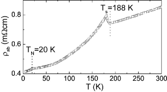
EuFe2As2 is special in the so-called “122” series (Fe2As2, with =Ba, Ca, Sr, or Eu, etc.) of iron pnictides, because it contains large local moments of Eu2+ ions (6.8 ) on site.YXiao_Eu Aside from the SDW/structural transition at =188 K, another transition at =20 K has been found which is associated with an type antiferromagnetic ordering of Eu2+ ions (see Fig. 1).Raffius1993 ; ZARen_Eu ; Chen_EuLa ; YXiao_Eu ; Herrero_Eu
To reach a comprehensive picture of the complex electronic structure in the SDW state of iron pnictides, and reveal the manifestation of various magnetic orderings on the electronic structure, we have performed the ARPES measurements of EuFe2As2 single crystals. Two hole Fermi pockets around and two electron pockets around are observed in the high-temperature paramagnetic (PM) state. In the SDW state, band splitting, folding, and hybridization are found to evolve with temperature. Detailed measurements reveal that the two small Fermi pockets symmetric about in the - direction are electronlike and holelike, respectively. This asymmetric electronic structure has not yet been reported in ARPES studies of iron pnictides, but is consistent with the quantum oscillation results by considering the different s for the two small pockets.Sebastian ; Analytis The drastic changes in electronic structure, i.e., the band splitting and the band shift, cannot be explained by a simple folding picture. In agreement with several studies by different techniques,YXiao_Eu ; Herrero_Eu ; Eu_optic no noticeable change in ARPES measurement is found across the antiferromagnetic transition of Eu2+ ordering.
II Experiment
High quality EuFe2As2 single crystals were synthesized by self-flux method, and more details can be found in Ref. Chen_EuLa, . Its stoichiometry was confirmed by energy dispersive x-ray (EDX) analysis. ARPES measurements were performed with randomly polarized 21.2 eV photons from a helium discharge lamp and with circularly polarized synchrotron light from Beamline 9 of Hiroshima synchrotron radiation center (HSRC). Scienta R4000 electron analyzers are equipped in both setups. The overall energy resolution is 9 meV, and angular resolution is 0.3∘. The samples were cleaved in situ, and measured in ultrahigh vacuum below 4 mbar. All data reported here were taken within 4 h after cleaving to minimize the aging effect. The high quality sample surface is confirmed by a clear pattern of low-energy electron diffraction (LEED). Most data presented here were taken with the helium discharge lamp unless otherwise specified.
III Results and discussions

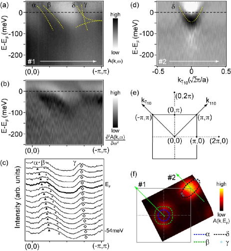
The electronic structure in the paramagnetic state is shown in Fig. 2, which is similar to other 122 compounds reported by ARPES measurements.ZX_PM ; Hasan_Sr Figures 2(a)-2(c) show the data of cut 1 [along - as indicated in Fig. 2(f)], where two holelike bands ( and ) can be identified. From the raw data [Fig. 2(a)] and the corresponding momentum distribution curves (MDCs) [Fig. 2(c)], an electronlike band () can be identified. Although the band bottom of is not resolved in the data, it may reach about 200 meV below the Fermi energy () by following its energy dispersion. In the second derivative data with respect to energy [Fig. 2(b)], the feature of is not resolved due to the large Fermi velocity. Nonetheless, there is another weak electronlike feature () near with smaller Fermi velocity and with band bottom at about 40-50 meV. Along -- [cut 2 in Fig. 2(d)], a parabolic electronlike band is observed with the band bottom at 45 meV below , which should be assigned to according to the position of the band bottom. Notice that photoemission intensity of the band is much less than that of along -, but this is reversed away from -, most likely caused by matrix element effects.Hasan_FeTe The resulting Fermi surfaces are depicted in Fig. 2(f), which consist of two hole pockets around , an elongated elliptical electron pocket around , and some Fermi crossings of around . Here the Fermi crossings may be originated from the second electron pocket which has been reported before in BaFe2As2 and SrFe2As2,ZX_PM ; Hasan_Sr although its complete shape cannot be determined from our data, likely due to matrix element effects. The measured Fermi surface topology, especially around , is in agreement with theoretical calculations for 122 compounds,Singh_calc ; Ma_calc ; Nekrasov_calc since the measured - direction in the two-dimensional (2D) BZ is closer to the - direction in the three-dimensional (3D) paramagnetic BZ under 21.2 eV light [Fig. 5(i)].
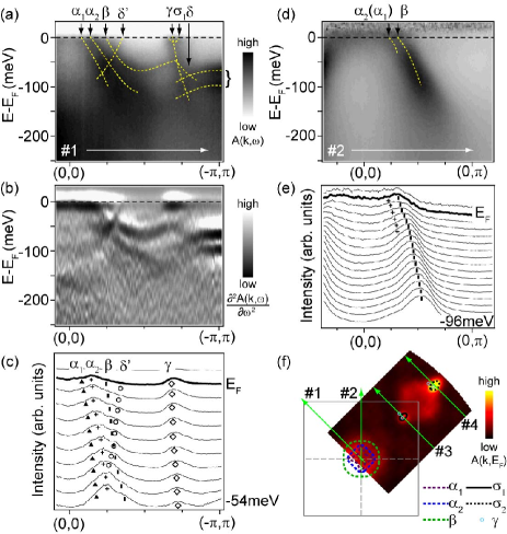
Figure 3 shows the electronic structure in the SDW state. Dispersions of various bands are shown as dashed lines in Figs. 3(a), 3(b), and 3(d). Comparing with the paramagnetic band structure, the band does not change along -. However, splits into and in the SDW state. In addition, the band hybridizes with , and a folded band () of appears around . Moreover, the feature around below in the paramagnetic state splits into two inverted parabolic bands in the SDW state [as denoted by the bracket in Fig. 3(a)], which are likely to be the dispersions from the split and bands. Along -, and are nearly degenerate, and folding is not resolved in this direction. , , , and around , and around are identified to cross by examining the MDCs in Figs. 3(c) and 3(e). As a result, the Fermi surface around consists of three hole Fermi pockets and a folded electron Fermi pocket. Again similar to the paramagnetic state, is not observable away from - due to the possible matrix element effects. As observed in the SDW state Fermi surface [Fig. 3(f)], a distinctive difference from the paramagnetic state Fermi surface is that two “bright spots” appear in the - direction near . As shown in Fig. 3(a), the hybridization of and results in a possible small electron band whose bottom is barely below , and gives a “bright spot” (the pocket) in the photoemission intensity map of the first BZ, which shall be given a zoom-in in Fig. 5. Thereby, no gap is found at in the electronic structure. Note that the bands are a result of the hybridization between the and bands. However, the band appears to cross the bands without any sign of hybridization. This is most likely due to their different symmetries with respect to certain mirror plane, as illustrated in Ref. YZhang_orbital, for the BaFe1.85Co0.15As2 in the paramagnetic state, where the band shows up only in -polarized geometry while the and bands show up only in the -polarized geometry. Therefore the and bands are both of odd symmetry, and thus the band from their hybridization may also be odd. On the other hand, the band is even. The opposite symmetries of and could result in the observed absence of hybridization here, assuming the symmetry properties of the bands are preserved in this series of iron pnictides.
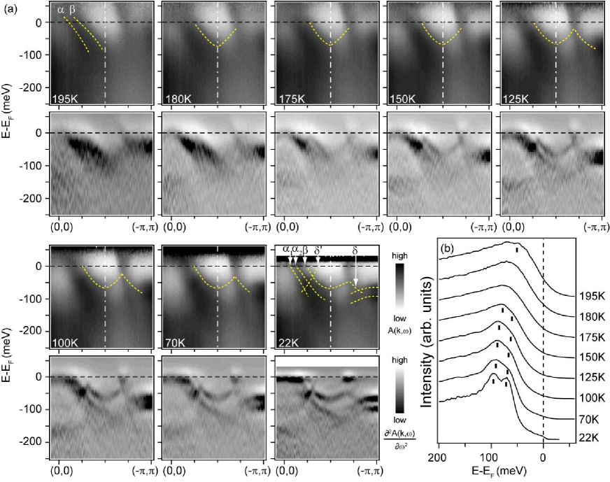
The evolution of electronic structure with temperature is illustrated in Fig. 4. As the temperature decreases from , the band appears to be symmetric with respect to the midway of - (the BZ boundary of the SDW state) due to the magnetic ordering in the SDW state. Nevertheless, the band becomes asymmetric as the temperature is further lowered to 22 K, since this band hybridizes with and therefore does not cross . This hybridization strengthens with decreasing temperature [Fig. 4(a)]. On the other hand, the band crosses the folded band with much weaker hybridization near the point. As observed before in other 122 systems,LXYang ; YZhang ; GDLiu ; ZX_SDW the band splitting is observed in this material as well. From the paramagnetic state to SDW state, the band near and the inverted parabolic band near split into , and two inverted parabolic bands correspondingly. The remarkable temperature dependence of the two inverted parabolic bands is shown in Fig. 4(b), where single energy distribution curves (EDCs) at the point are stacked. At 22 K, the two peaks are at 70 and 95 meV below , respectively, which correspond to the band tops of the two inverted parabolic bands. Both bands move toward with increasing temperature, and merge into one broad feature in the paramagnetic state. When two features are distinguishable, their separation decreases slightly with increasing temperature. If considering a simple folding picture as suggested in Ref. Hasan_Sr, , it cannot reproduce the complex band structure in the SDW state, especially inadequate to explain the splitting and shift of bands.ZX_SDW Therefore, local exchange interactions are suggested to be included to explain the electronic structure.LXYang ; YZhang
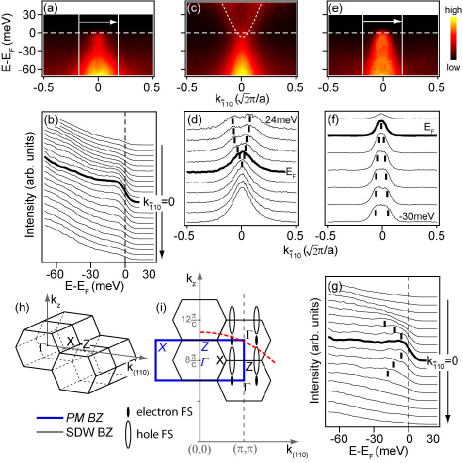
To further investigate the nature of the “bright spots”, a cut perpendicular to - and across the pocket is measured as indicated by cut 3 in Fig. 3(f). In data taken at 22 K [Figs. 5(a) and 5(b)], a hump is observed near around =0, indicating most probably a small electron pocket. To further elucidate this, additional data were taken at higher temperature (175 K) but still in the SDW state and shown in Figs. 5(c) and 5(d). Figure 5(c) shows the photoemission intensity divided by the energy-resolution-convoluted Fermi-Dirac function. It reveals a parabolic electron band in the vicinity of . The corresponding MDCs are shown in Fig. 5(d), where markers indicate the dispersion of the electron band. The separated two peaks above merge into a single peak slightly below , indicating that this electron band indeed crosses .
Similarly, data were taken along a cut through the “bright spot” near outside the first BZ [cut 4 indicated in Fig. 3(f)]. Interestingly, a dispersion that gives a hole Fermi pocket is observed in the spectrum image plot, EDCs, and MDCs [Figs. 5(e)-5(g)]. These results indicate that the two small pockets symmetric about are electronlike and holelike respectively. This asymmetric electronic structure can be understood by realizing the variation in the Fermi surface. Figure 5(h) presents a 3D SDW folded BZ, and Fig. 5(i) shows the corresponding SDW BZ together with the paramagnetic BZ in the plane. Along the in-plane direction, Fermi surfaces are depicted in Fig. 5(i) that pairs of small electron and hole pockets are symmetric about and , respectively, whereas a dashed curve is a schematic constant energy cut through an electron pocket and a hole pocket near . This scenario naturally explains our result, and is in qualitative agreement with quantum oscillations of 122 compounds, which indicate the existence of small electron and hole Fermi pockets aligned along .Sebastian ; Analytis
The estimated Luttinger volume of the , , and Fermi pockets near are 1.7%, 3.6%, and 9.5% of the paramagnetic BZ, respectively. The tiny and pockets near both comprise less than 0.5% of the paramagnetic BZ. These results agree well with the quantum oscillation measurements for the small Fermi pockets (, , and ). However, quantum oscillations did not find the large Fermi surfaces ( and ). This might be due to the fact that the electrons could not finish circulating the large pocket before they are scattered by impurities.
To understand the detailed electronic structure evolution near , a series of the second derivative image plots are presented in Fig. 6(b). Away from cut 6, the two -like features move toward the higher energies and become blurred. Features at are only visible near the two “bright spots”. Although the Fermi surface mapping shows patch-like features near other than the two “bright spots” [Fig. 6(a)], the patch is just remnant spectral weight from bands below . As shown in cuts 5 and 5-7 of Fig. 6(b), the maxima of two -like features are below , therefore these features do not cross . Similar to the observations made in BaFe2As2,ZX_SDW ; GDLiu it is observed that the electronic structure shows saddle-surface-like features near below , as seen in Fig. 3(a) and cut 6 in Fig. 6(b). Band tops of the two inverted parabolic bands coincide with band bottoms of the two parabolic bands, therefore they are the same bands split from the paramagnetic bands. Unlike the presence of the band along - in Fig. 3(a), it is absent along the direction perpendicular to - [cuts 5-7 in Fig. 6(b)]. However, it is observed in a similar direction measured with 10 eV synchrotron light [Fig. 7(b)]. Therefore it is indeed a manifestation of matrix element effects that little photoemission intensity of is detected away from - under the experimental setup of helium lamp.
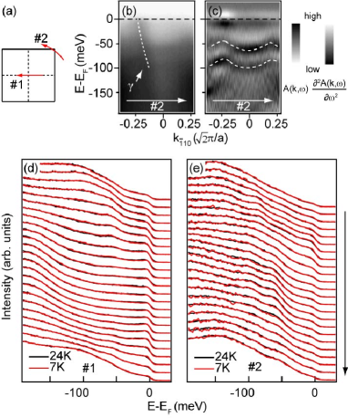
Since the Eu2+ ions in EuFe2As2 undergo an antiferromagnetic transition at a Neel temperature of =20 K, it is thus straightforward to investigate the electronic structure below and above this transition. Figures 7(b) and 7(c) present the photoemission intensities and the corresponding second derivative around taken at 7 K with 10 eV photons. The band and two -like bands are clearly observed. The band bottoms of the -like bands are situated at the same energies as those measured with 21.2 eV photons. Since the ARPES spectra are much more bulk sensitive when measured with 10 eV photons, the match between 21.2 eV data and 10 eV data suggests that the shift and splitting of the two parabolic (or inverted) bands near are not just surface effect, but reflecting bulk properties. Figures 7(d) and 7(e) show the EDCs around and , respectively, both below and above . Across , no observable change except the thermal broadening has been observed within the accuracy allowed by the energy resolution of 8 meV. In Ref. Chen_EuLa, , it was found that the -type antiferromagnetism can be converted to ferromagnetism with a magnetic field as small as 1.5 T and the inter-layer coupling was estimated to be 0.46-0.69 meV, which is one order of magnitude lower than our resolution. This shows that the electronic structure near is not altered noticeably by the ordering of the Eu2+ moments; on the other hand, even if there were certain subtle effects of the magnetism, they cannot be easily detected in our ARPES measurements, as limited by the current energy resolution. Nonetheless, magnetism or fluctuations may play an important role to mediate superconductivity, noting that Eu1-xLaxFe2As2 is not superconducting,Chen_EuLa while Eu1-xKxFe2As2 is superconducting where long-range magnetic ordering is killed.Jeevan_EuK
IV Conclusion
In conclusion, we have presented in detail the electronic structure of EuFe2As2 both in the paramagnetic state, the SDW state, and the antiferromagnetically ordered state of the Eu2+ moments. The temperature evolution of the band dispersion across reveals that the band folding and splitting are established in the SDW state. The folded band hybridizes with and the hybridization gap opens as the temperature decreases. In addition, this hybridization gives rise to a small electron band near in the first BZ. However, the similar small pocket outside the first BZ is proved to be holelike. This gives a natural explanation of the observation of quantum oscillation measurements. A simple folding picture cannot describe the significant change in the electronic structure in the SDW state. The experiment by more bulk sensitive ARPES with 10 eV light provides evidence that the band splitting is not due to any surface effect, such as a surface reconstruction. The undetectable change in electronic structure across suggests the weak electronic coupling between Eu sublattice and FeAs sublattice.
During the preparation of this paper, we noticed that another ARPES study of EuFe2As2 has been posted online.ARPES_Eu Most experimental results of both papers are consistent with each other, although the determined Fermi surfaces are not exactly the same, probably due to different s.
Acknowledgements.
Some of the preliminary data (not shown here) were taken at ELETTRA synchrotron light source. This work was supported by the NSFC, MOE, MOST (National Basic Research Program No. 2006CB921300), STCSM of China, and the NSF of U.S. under Grant No. PHY-0603759, and ICTP-ELETTRA project.References
- (1) Y. Kamihara, T. Watanabe, M. Hirano, and H. Hosono, J. Am. Chem. Soc. 130, 3296 (2008).
- (2) X. H. Chen, T. Wu, G. Wu, R. H. Liu, H. Chen, and D. F. Fang, Nature (London) 453, 761 (2008).
- (3) Z. A. Ren, W. Lu, J. Yang, W. Yi, X.-L. Shen, Z. Cai, G.-C. Che, X.-L. Dong, L.-L. Sun, F. Zhou, and Z.-X. Zhao, Chin. Phys. Lett. 25, 2215 (2008).
- (4) R. H. Liu, G. Wu, T. Wu, D. F. Fang, H. Chen, S. Y. Li, K. Liu, Y. L. Xie, X. F. Wang, R. L. Yang, L. Ding, C. He, D. L. Feng, and X. H. Chen, Phys. Rev. Lett. 101, 087001 (2008).
- (5) C. Wang, L.-J. Li, S. Chi, Z.-W. Zhu, Z. Ren, Y.-K. Li, Y.-T. Wang, X. Lin, Y.-K. Luo, S. Jiang, X.-F. Xu, G.-H. Cao, and Z. A. Xu, EPL 83, 67006 (2008).
- (6) M. Rotter, M. Tegel, D. Johrendt, I. Schellenberg, W. Hermes, and R. Pöttgen, Phys. Rev. B 78, 020503(R) (2008).
- (7) M. Rotter, M. Tegel, and D. Johrendt, Phys. Rev. Lett. 101, 107006 (2008).
- (8) G. Wu, R. H. Liu, H. Chen, Y. J. Yan, T. Wu, Y. L. Xie, J. J. Ying, X. F. Wang, D. F. Fang, and X. H. Chen, EPL 84, 27010 (2008).
- (9) K. Sasmal, B. Lv, B. Lorenz, A. M. Guloy, F. Chen, Y.-Y. Xue, and C.-W. Chu, Phys. Rev. Lett. 101, 107007 (2008).
- (10) G. Wu, H. Chen, T. Wu, Y. L. Xie, Y. J. Yan, R. H. Liu, X. F. Wang, J. J. Ying, and X. H. Chen, J. Phys.: Condens. Matter 20, 422201 (2008).
- (11) Y.-P. Qi, Z.-S. Gao, L. Wang, D.-L. Wang, X.-P. Zhang, and Y.-W. Ma, New. J. Phys. 10, 123003 (2008).
- (12) H. S. Jeevan, Z. Hossain, D. Kasinathan, H. Rosner, C. Geibel, and P. Gegenwart, Phys. Rev. B 78, 092406 (2008).
- (13) Anupam, P. L. Paulose, H. S. Jeevan, C. Geibel, and Z. Hossain, J. Phys.: Condens. Matter 21, 265701 (2009).
- (14) H. Chen, Y. Ren, Y. Qiu, W. Bao, R. H. Liu, G. Wu, T. Wu, Y. L. Xie, X. F. Wang, Q. Huang, and X. H. Chen, EPL 85, 17006 (2009).
- (15) Y. Zhang, J. Wei, H. W. Ou, J. F. Zhao, B. Zhou, F. Chen, M. Xu, C. He, G. Wu, H. Chen, M. Arita, K. Shimada, H. Namatame, M. Taniguchi, X. H. Chen, and D. L. Feng, Phys. Rev. Lett. 102, 127003 (2009).
- (16) L. X. Yang, Y. Zhang, H. W. Ou, J. F. Zhao, D. W. Shen, B. Zhou, J. Wei, F. Chen, M. Xu, C. He, Y. Chen, Z. D. Wang, X. F. Wang, T. Wu, G. Wu, X. H. Chen, M. Arita, K. Shimada, M. Taniguchi, Z. Y. Lu, T. Xiang, and D. L. Feng, Phys. Rev. Lett. 102, 107002 (2009).
- (17) G.-D. Liu, H.-Y. Liu, L. Zhao, W.-T. Zhang, X.-W. Jia, J.-Q. Meng, X.-L. Dong, J. Zhang, G. F. Chen, G.-L. Wang, Y. Zhou, Y. Zhu, X.-Y. Wang, Z.-Y. Xu, C.-T. Chen, and X. J. Zhou, Phys. Rev. B 80, 134519 (2009).
- (18) M. Yi, D. H. Lu, J. G. Analytis, J.-H. Chu, S.-K. Mo, R.-H. He, M. Hashimoto, R. G. Moore, I. I. Mazin, D. J. Singh, Z. Hussain, I. R. Fisher, and Z.-X. Shen, Phys. Rev. B 80, 174510 (2009).
- (19) D. Hsieh, Y. Xia, L. Wray, D. Qian, K. K. Gomes, A. Yazdani, G. F. Chen, J. L. Luo, N. L. Wang, and M. Z. Hasan, arXiv:0812.2289 (unpublished).
- (20) W. Z. Hu, J. Dong, G. Li, Z. Li, P. Zheng, G. F. Chen, J. L. Luo, and N. L. Wang, Phys. Rev. Lett. 101, 257005 (2008).
- (21) S. E. Sebastian, J. Gillett, N. Harrison, P. H. C. Lau, D. J. Singh, C. H. Mielke, and G. G. Lonzarich, J. Phys.: Condens. Matter 20, 422203 (2008).
- (22) J. G. Analytis, R. D. McDonald, J.-H. Chu, S. C. Riggs, A. F. Bangura, C. Kucharczyk, M. Johannes, and I. R. Fisher, Phys. Rev. B 80, 064507 (2009).
- (23) S. J. Moon, J. H. Shin, D. Parker, W. S. Choi, I. I. Mazin, Y. S. Lee, J. Y. Kim, N. H. Sung, B. K. Cho, S. H. Khim, J. S. Kim, K. H. Kim, and T. W. Noh, arXiv:0909.3352 (unpublished).
- (24) L. de Medici, S. R. Hassan, and M. Capone, J. Supercond. Novel Magn. 22, 535 (2009).
- (25) M. D. Johannes and I. I. Mazin, Phys. Rev. B 79, 220510(R) (2009).
- (26) Y. Xiao, Y. Su, M. Meven, R. Mittal, C. M. N. Kumar, T. Chatterji, S. Price, J. Persson, N. Kumar, S. K. Dhar, A. Thamizhavel, and Th. Brueckel, Phys. Rev. B 80, 174424 (2009).
- (27) T. Wu, G. Wu, H. Chen, Y. L. Xie, R. H. Liu, X. F. Wang, and X. H. Chen, J. Magn. Magn. Mater. 321, 3870 (2009).
- (28) H. Raffius, E. Mörsen, B. D. Mosel, W. Müller-Warmuth, M. Jeitschko, L. Terbüchte, and T. Vomhof, J. Phys. Chem. Solids 54, 135 (1993).
- (29) Z. A. Ren, Z.-W. Zhu, S. Jiang, X.-F. Xu, Q. Tao, C. Wang, C.-M. Feng, G. H. Cao, and Z. A. Xu, Phys. Rev. B 78, 052501 (2008).
- (30) J. Herrero-Martín, V. Scagnoli, C. Mazzoli, Y.-X. Su, R. Mittal, Y.-G. Xiao, T. Brueckel, N. Kumar, S. K. Dhar, A. Thamizhavel, and L. Paolasini, Phys. Rev. B 80, 134411 (2009).
- (31) D. Wu, N. Barišić, N. Drichko, S. Kaiser, A. Faridian, M. Dressel, S. Jiang, Z. Ren, L. J. Li, G. H. Cao, Z. A. Xu, H. S. Jeevan, and P. Gegenwart, Phys. Rev. B 79, 155103 (2009).
- (32) M. Yi, D. H. Lu, J. G. Analytis, J.-H. Chu, S.-K. Mo, R.-H. He, R. G. Moore, X. J. Zhou, G. F. Chen, J. L. Luo, N. L. Wang, Z. Hussain, D. J. Singh, I. R. Fisher, and Z.-X. Shen, Phys. Rev. B 80, 024515 (2009).
- (33) Y. Xia, D. Qian, L. Wray, D. Hsieh, G. F. Chen, J. L. Luo, N. L. Wang, and M. Z. Hasan, Phys. Rev. Lett. 103, 037002 (2009).
- (34) D. J. Singh, Phys. Rev. B 78, 094511 (2008).
- (35) F.-J. Ma, Z.-Y. Lu, and T. Xiang, Front. Phys. China. (to be published).
- (36) I. A. Nekrasov, Z. V. Pchelkina, and M. V. Sadovskii, Pis’ma Zh. Eksp. Teor. Fiz. 88, 155 (2008) [JETP Lett. 88, 144 (2008)].
- (37) Y. Zhang, B. Zhou, F. Chen, J. Wei, M. Xu, L. X. Yang, C. Fang, W. F. Tsai, G. H. Cao, Z. A. Xu, M. Arita, H. Hayashi, J. Jiang, H. Iwasawa, C. H. Hong, K. Shimada, H. Namatame, M. Taniguchi, J. P. Hu, D. L. Feng, arXiv:0904.4022v2 (unpublished).
- (38) S. de Jong, E. van Heumen, S. Thirupathaiah, R. Huisman, F. Massee, J. B. Goedkoop, R. Ovsyannikov, J. Fink, H. A. Dürr, A. Gloskovskii, H. S. Jeevan, P. Gegenwart, A. Erb, L. Patthey, M. Shi, R. Follath, A. Varykhalov, and M. S. Golden, EPL 89, 27007 (2010).