e-mail opel@wmi.badw.de, Phone: +49-89-289-14237, Fax: +49-89-289-14206
2 Institut für Anorganische Chemie, Universität Bonn, 53117 Bonn, Germany
3 Physik-Department, Technische Universität München, 85748 Garching, Germany
XXXX
Novel Multifunctional Materials Based on Oxide Thin Films and Artificial Heteroepitaxial Multilayers
Abstract
\abstcolTransition metal oxides show fascinating physical properties such as high temperature superconductivity, ferro- and antiferromagnetism, ferroelectricity or even multiferroicity. The enormous progress in oxide thin film technology allows us to integrate these materials with semiconducting, normal conducting, dielectric or non-linear optical oxides in complex oxide heterostructures, providing the basis for novel multi-functional materials and various device applications. Here, we report on the combination of ferromagnetic, semiconducting, metallic, and dielectric materials properties in thin films and artificial heterostructures using laser molecular beam epitaxy. We discuss the fabrication and characterization of oxide-based ferromagnetic tunnel junctions, transition metal-doped semiconductors, intrinsic multiferroics, and artificial ferroelectric/ferromagetic heterostructures - the latter allow for the detailed study of strain effects, forming the basis of spin-mechanics. For characterization we use X-ray diffraction, SQUID magnetometry, magnetotransport measurements, and advanced methods of transmission electron microscopy with the goal to correlate macroscopic physical properties with the microstructure of the thin films and heterostructures.
pacs:
81.15.Fg, 68.37.Og, 85.75.-d, 75.50.Pp, 77.55.Nv[height=6cm]abstract \titlefigurecaption The combination of magnetic properties with dielectric, semiconducting, or ferroelectric materials in one and the same material (e.g. magnetic semiconductors (MS) or intrinsic multiferroics) as well as in artificial heterostructures (e.g. ferromagnetic/dielectric heterostructures for magnetic tunnel junctions (MTJs) or artificial multiferroic heterostructures) allows for the design of materials with novel functionalities and provides the basis for various device applications.
1 Introduction.
Oxide materials are in the focus of intense research activities (see e.g. Refs. [1, 2] for recent reviews) since more than two decades. On the one hand, they show a large variety of interesting and in some cases unique physical properties. Prominent examples are the cuprate superconductors [3], ferroelectrics [4], non-linear optical materials, electrically controllable dielectrics [5], the colossal magnetoresistance manganites [6, 7], or multiferroic materials [8, 9]. On the other hand, oxides offer a broad potential for device applications. Although the underlying physics of some oxide materials is still under debate (e.g. high-temperature superconductivity), they are widely used in applications. A particularly promising research direction is the integration of the outstanding properties of different oxides in complex heterostructures to achieve materials with improved or extended functionalities. Such materials may pave the way for novel device structures. Notable examples are ferroelectric field-effect transistors, controllable dielectric microwave devices, superconducting high-frequency modules, magnetoresistive sensors, or electrically controllable and readable magnetic random access memories.
An obvious approach for the realization of oxide materials with improved functionality is the integration of two properties in one and the same material. Well known examples are ferromagnetic semiconductors [10, 11, 12] combining semiconducting and ferromagnetic properties or intrinsic multiferroics [8, 9] having a finite ferromagnetic and ferroelectric order parameter. However, the realization of such intrinsically multi-functional materials turns out to be difficult, in particular when room temperature operation is required. Another promising approach for the realization of multi-functional materials is the integration of oxides with different properties in artificial heterostructures. This approach has become feasible with the enormous progress in oxide thin film technology over the last two decades. For example, today laser molecular beam epitaxy (laser-MBE) employing in-situ reflection high energy electron diffraction (RHEED) allows us to grow oxide thin films with crystalline quality approaching semiconductor standards [13, 14, 15, 16]. Moreover, in close analogy to GaAs/AlAs heteroepitaxy it is possible to grow complex heterostructures composed of different oxides on suitable substrates in a layer-by-layer or block-by-block mode [13, 17].
The successful heteroepitaxial growth of oxide materials in complex multilayers opens various possibilities to deliberately tailor their physical properties and to generate new functionalities. First, in analogy to semiconductor heterostructures band gap engineering can be employed to tailor the band structure at the interfaces. A prominent example is the system LaAlO3/SrTiO3, forming a two-dimensional electron gas at the interface [18] which shows superconductivity below 200 mK [19]. Band bending effects due to interface charges may also play an important role in ferromagnet/ferroelectric/ferromagnet tunnel junctions, resulting in differences of the tunneling resistance dependent on the polarization direction in the ferroelectric tunneling barrier [20, 21]. Second, magnetic oxide heterostructures may allow to tailor the magnetic interactions at the interfaces thereby providing the basis for deliberate spin engineering. In this way novel magnetic properties can be designed by varying the layer structures. However, since the magnetic interactions in most cases are short range, this approach requires good control of the interfaces on an atomic scale, making controlled spin engineering very demanding. Third, heteroepitaxial multilayers in most cases involve epitaxial coherency strain. This can be used to deliberately tailor the materials properties in heterostructures by strain. Strain effects have been successfully applied to superconducting [14, 22], magnetoresistive [23, 24, 25, 26], ferromagnetic [27, 28, 29], and ferroelectric materials [30, 31]. Fourth, so-called asymmetric superlattices such as BaTiO3/SrTiO3/CaTiO3 can be used to break inversion symmetry. In this way improved ferroelectric and non-linear optical properties can be obtained [32, 33, 34]. Finally, superlattices of materials possessing different types of order parameter (e.g. superconducting, ferromagnetic, ferroelectric) can be fabricated, allowing for the coupling of the order parameters at the interfaces. Although this coupling in many cases is not well understood, it led to applications in which a single property, such as magnetization or electrical conductivity, can controllably be turned on and off [35, 36]. Along with many experimental achievements, a growing number of theory predictions has been published regarding artificial material systems based on heterostructures [37, 38, 39, 40, 41, 42].
In this article, we restrict our discussion to heterostructures based on magnetic oxides. We review our results obtained within the priority program 1157 of the German Research Foundation. Magnetic materials and heterostructures have achieved broad attention due to their interesting physics and their versatile application in the field of magneto and spin electronics [43, 44, 45]. In this context ferromagnetic oxides are of particular interest since some of them are expected to show an almost complete spin polarization at the Fermi edge or are considered as ferromagnetic insulators. Interesting material systems are magnetite (Fe3O4) and the double perovskites with composition O6 ( alkaline earth, , magnetic or nonmagnetic transition metal ion) as they show Curie temperatures well above room temperature and band structure calculations predict half-metallic behavior. This makes them well suited as electrode materials for spin injection into semiconductors or the realization of magnetic tunnel junctions with a high tunneling magnetoresistance [46, 47]. We have successfully grown epitaxial thin films of these material classes [17, 48, 49, 50, 51] and clarified several physical aspects such as the magnetic exchange [52, 53, 54, 55] or the influence of strain and steric effects [50, 56, 57, 58]. Here, we report on the growth and characterization of magnetic oxides and the integration of such oxides with semiconducting, normal conducting, dielectric and ferroelectric materials in artificial heterostructures. Special emphasis will be put on (i) magnetic tunnel junctions consisting of ferromagnetic, dielectric, and normal conducting layers [47], (ii) transition metal-doped semiconductors [59], and (iii) multiferroic materials [60]. Along with their integral physical properties such as electrical conductivity, magnetoresistance, or magnetization we present data on their microscopic structure with a special emphasis on surface and interface quality obtained by high-resolution X-ray diffraction techniques and advanced methods of transmission electron microscopy.
2 Magnetic Tunnel Junctions Based on Fe3O4.
Magnetic tunnel junctions (MTJs) are key elements for the realization of non-volatile magnetic random access memory (MRAM) devices [61], magnetic sensors, or programmable logic elements [62]. MTJs based on simple ferromagnetic metals and alloys are well known for many years. The tunneling magnetoresistive (TMR) effect was first reported in 1975 in Fe/GeOx/Co MTJs [63]. Here, , with and denoting the tunnel resistance for the antiparallel and parallel magnetization direction, respectively. While at room temperature the achieved TMR values could be increased up to around 10% in the following years [64], it was predicted in 2000 that a further dramatic increase should be possible for Fe/MgO/Fe MTJs using highly textured MgO(100) tunneling barriers due to the Bloch state filtering of the electronic wave functions [65, 66]. Indeed, in 2004 a high TMR effect above 200% was reported for Fe [67] or CoFe electrodes [68], and today % is observed in CoFeB/MgO/CoFeB MTJs at room temperature [69].
Very high TMR values are expected for MTJs based on half-metallic ferromagnets even without wave function filtering, requiring highly textured tunneling barriers. Along this line, magnetite (Fe3O4) is a promising candidate, because band structure calculations predict half-metallicity even at room temperature [70]. Moreover, magnetite has a high Curie temperature of 860 K allowing for room temperature applications [71]. Indeed, spin-resolved photoelectron spectroscopy experiments on magnetite thin films revealed a spin polarization near the Fermi level of up to 80% at room temperature [72, 73]. In contrast, the room temperature TMR effects of magnetite based MTJs are below 20%. A summary of recent results is given in Table 1 [74, 75, 76, 77, 78, 79]. Therefore, it is important to study the behavior of magnetite at the electrode-barrier interface, the influence of the tunneling barrier itself, and the magnetic coupling through thin barriers.
| Fe3O4 | barrier | counter | TMR | Ref. |
| orientation | electrode | (%) | ||
| (001) | MgO | CoO | 0.4 | [75] |
| (001) | MgO | CoCr2O4 | 0.5 | [76] |
| polycrystalline | AlOx | NiFe | 7 | [77] |
| (110) | AlOx | CoFe | 10 | [78] |
| polycrystalline | AlOx | Co | 13 | [79] |
| (110) | AlOx | CoFe/NiFe | 14 | [74] |
| (001) | AlOx | Co | 20 | this work |
We have fabricated MTJs based on epitaxial magnetite thin films. Five different materials (MgO, SrTiO3, NdGaO3, SiO2, and AlOx) have been used for the tunneling barrier. Polycrystalline Ni and Co films deposited by electron beam evaporation in the same ultra-high vacuum cluster system served as counter electrodes. According to recent tunneling experiments [64], Ni and Co have spin polarizations of 33% and 42%, respectively. The magnetic properties of the magnetic heterostructures, in particular the presence of any magnetic coupling between the ferromagnetic junction electrodes across the tunneling barrier, was studied by SQUID magnetometry prior to pattering of the samples. The magnetotransport behavior of the MTJs was measured as a function of temperature and applied magnetic field using a standard four probe technique.
2.1 Fabrication Process.
The thin film heterostructures required for the magnetite based MTJs were fabricated in an ultra-high vacuum (UHV) cluster system. First, the bottom electrode consisting of epitaxial TiN and a 20 to 50 nm thick Fe3O4 layer were deposited on (001) oriented MgO substrates using laser-MBE [13, 15]. Stoichiometric targets and a KrF excimer laser (248 nm) with a fluence of 2 J/cm2 have been used. The TiN layer was grown at a substrate temperature of 600∘C and Fe3O4 was deposited at 300∘C, both at an Ar pressure of mbar. The growth was monitored in-situ using RHEED. Details of the deposition process including the infrared laser substrate heating are given elsewhere [13, 15, 17, 80].
Second, the thin insulating tunneling barrier is deposited. Five different materials were used: MgO, SrTiO3, and NdGaO3 have been grown by pulsed laser deposition (PLD) from stoichiometric targets, again in a pure Ar atmosphere of mbar and a substrate temperature of 330∘C. SiO2 was deposited by electron beam evaporation in the same UHV cluster system at room temperature without breaking the vacuum. The AlOx tunneling barriers were obtained by evaporating Al also in the same UHV cluster system and subsequent oxidation in pure O2. The only material growing epitaxially on Fe3O4 was MgO as confirmed by the corresponding RHEED pattern.111Epitaxial growth of MgO by PLD was also achieved at room temperature in an Ar/O2 mixture (99:1) at mbar. The SrTiO3, NdGaO3, SiO2, and AlOx thin films form polycrystalline tunneling barriers on Fe3O4.
Third, a 40 nm thin Ni or Co top electrode serving as the ferromagnetic counter electrode of the MTJs was deposited in-situ by electron beam evaporation in the UHV cluster system at room temperature. Due to the epitaxial nature of the MgO tunneling barrier, also epitaxial magnetite counter electrodes have been used for this barrier type. Finally, for most samples an in-situ Au layer was deposited also by e-beam evaporation to prevent the oxidation of the ferromagnetic top electrode during the patterning process. We used an in-situ atomic force microscope to probe the surface quality. The structural quality and layer thicknesses of the films was determined with a Bruker-AXS high-resolution X-ray diffractometer.
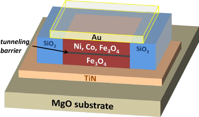
The multilayer stacks (cf. Fig. 1) were used to fabricate MTJs with different junction areas and shapes by optical lithography and Ar ion beam milling [81]. In a first step, a wide strip is patterned into the whole stack. Then, a rectangular or ring-shaped junction area is defined by etching a mesa structure using an adequately shaped photoresist stencil as the etching mask. The removed part is replaced by a polycrystalline SiO2 window insulation, using the same resist stencil for the lift-off process. Finally, a narrow Au strip is used to provide the electrical contacts to the top electrode. In this way rectangular MTJs with areas ranging from to and ring-shaped MTJs with inner (outer) diameters of () and () have been fabricated.
2.2 Magnetic Characterization of the Junction Electrodes.
First, a detailed characterization of the magnetite films was performed. The Fe3O4 thin films were found to show properties which are comparable to those of single crystal bulk material with respect to crystallographic structure and magnetization [82, 83]. In particular, their magnetization versus temperature curves showed a pronounced Verwey transition [84] confirming the high structural quality and indicating perfect stoichiometry [85].
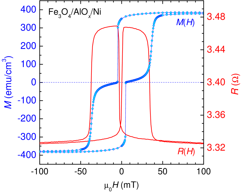
Next, magnetization versus applied magnetic field curves, , of the multilayer stacks prior to any photolithographic processing and patterning have been measured in a SQUID magnetometer at different temperatures. The magnetic field was applied parallel to the layers. In this way the values of the coercive field and saturation magnetization in the bottom and counter electrode can be determined. Furthermore, the presence of a finite magnetic coupling across the tunneling barrier can be checked. Figure 2 (blue curve, left scale) shows the curve of a sample consisting of 14 nm TiN, 52 nm Fe3O4, 2.5 nm AlOx, and 40 nm Ni at 210 K. Obviously, the magnetization of the bottom and counter electrode switches separately at different fields. From the experimental data the coercivities of the Ni and the Fe3O4 layer are determined to 5 mT and 32 mT at 210 K, respectively. These values decrease to 2 mT and 24 mT, respectively, at 380 K (not shown here). Due to the strong difference of the coercive fields an antiparallel magnetization orientation of the bottom and counter electrode is achieved over a wide field range. This is a prerequisite for a reliable determination of the TMR value without using an exchange bias layer. Furthermore, the clear step-like shape of the curves (cf. Fig. 2, blue) at all temperatures between 210 K and 380 K indicates a homogeneous switching of the magnetization direction in the junction electrodes. This is necessary for achieving an optimum TMR effect. Both the gradual rotation of magnetic domains and a glass-like magnetic state would be unfavorable in this respect.
Comparing the coercive field of the Ni counter electrode in Fig. 2 to that of a 20 nm thick reference Ni film (0.25 mT at 290 K), we found an increase of about a factor of 10. This effect is attributed to a residual magnetic coupling through the thin insulating barrier. Comparing curves of stacks with different barrier materials, we find slightly sharper switching steps for SiO2 than for AlOx. This indicates a more homogeneous switching of the magnetic domains. On the other hand, the barrier thickness is more difficult to control for SiO2 than for AlOx. For MgO barriers, the difference between the coercive fields of the Fe3O4 bottom and the Fe3O4/Ni counter electrode amounts to only about 7 mT at room temperature. At lower temperatures (210 K and 150 K) the electrodes even switch together at approximately 30 mT. That is, the stack behaves like a single ferromagnetic layer. This provides strong evidence for a strong coupling of the ferromagnetic electrodes across the MgO barrier layer. Further details on TiN/Fe3O4/MgO/Fe3O4/Au MTJs are discussed in subsection 2.5. In the following subsection we first focus on MTJs based on TiN/Fe3O4/AlOx/(Ni;Co)/Au stacks.
2.3 Magnetotransport Properties.
The magnetotransport measurements of the MTJs were performed using a standard four-probe technique in a liquid He cryostat system with variable temperature insert and a 10 T superconducting solenoid. For each magnetic field value (or temperature), the voltage drop across the MTJs was measured with different polarities of the applied current to eliminate possible thermovoltages. The magnetic field was always applied in the film plane. We note that the resistivity of the TiN films is much smaller than that of the magnetite film. Therefore, this layer serves as a low resistance shunt of the magnetite layer in the bottom electrode. In the junction area the electrical current is flowing vertically from the bottom TiN layer through the ferromagnetic bottom electrode (Fe3O4) across the tunneling barrier to the ferromagnetic top electrode (Ni or Co). Finally, the current is leaving the junction area via the Au wiring layer.
Tunneling Resistance.
Information on the on-chip homogeneity of the tunneling barrier can be obtained by comparing the resistance times area product, , of junctions patterned on the same chip. In Table 2 we have listed the room temperature values of junctions with different area but the same thickness ( nm) of the AlOx tunneling barrier. As expected for a spatially homogeneous barrier, we find or, equivalently, We found that the junctions with higher values show a significantly larger TMR [86]. We note that the values found for the AlOx barrier in our experiment are lower than those observed by other groups [87], but comparable to those reported for a lower barrier thickness [86]. This can be explained by assuming a smaller oxide thickness in our AlOx or may point to the presence of defect states in our barrier, as suggested by the behavior which will be discussed in the following.
| area () | () | () |
|---|---|---|
| 66 | ||
| 36 | ||
| 23 |
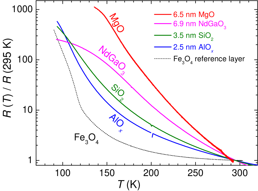
Figure 3 shows normalized resistance versus temperature curves, , obtained for MTJs with five different barrier materials. For comparison we also show the normalized curve of a magnetite thin film. The absolute resistance values vary between about 5 to at room temperature, depending on the barrier type and junction area. Due to the Verwey transition at K [84], the resistance of the magnetite layer increases strongly below this temperature.
Figure 3 clearly shows a strong increase of the junction resistance with decreasing temperature. In contrast, for an ideal tunneling barrier with barrier higher much larger than we expect only a slight increase of the tunneling resistance due to the reduction of the smearing of the Fermi distribution with decreasing temperature. This indicates that all tunneling barriers are far from being ideal and most likely have a considerable density of defect states mediating thermally activated inelastic tunneling. According to the data of Fig. 3, this effect is strongest for the MgO and weakest for the AlOx barrier, suggesting that the MgO barrier has the highest and the AlOx the lowest density of defect states. We note that the MgO, SrTiO3, and NdGaO3 barriers are deposited by PLD from stoichiometric targets in pure Ar atmosphere to avoid oxidation of the Fe3O4 base electrode. This is known to result in oxygen deficiency and, in turn, defect states in the barrier layer. The AlOx barrier, however, is obtained by evaporation of Al and subsequent oxidation in pure oxygen atmosphere. As pointed out above, for the MTJs with the MgO barrier magnetic coupling of the junction electrodes is observed despite the large barrier thickness of 6.5 nm. This coupling may be mediated by the high density of defect states in the barrier together with an Fe doping of the barrier layer by interdiffusion. Although this scenario is quite likely, a more detailed study is required to clarify this issue.
We also have to address the contribution of the magnetite layer to the measured junction resistance. Assuming a homogeneous current feeding into the junction through the well conducting TiN bottom layer, the resistance of the magnetite layer for the current perpendicular to plane configuration is estimated to at room temperature for a junction area of . Here, we use the measured resistivity and thickness of the magnetite layer. Comparing this value with the total junction resistance we see that the additional resistance of the magnetite layer is negligible in most cases, at least at temperatures well above the Verwey transition temperature. As will be pointed out below, there are situations where the influence of the magnetite electrode has to be taken into account. In this case, unusually high effective TMR values can be obtained due to current redistribution.
Tunneling Magnetoresistance.
From the measured curves we have determined the TMR effect
| (1) |
for MTJs with different barrier materials in the temperature regime between 150 K and 350 K. Here, is the resistance corresponding to the maximum resistance of the respective MTJ. is the resistance for the parallel magnetization configuration. For the evaluation of we always used the junction resistance measured at mT for . All investigated samples reproducibly show a positive TMR effect. Furthermore, the curves are symmetric with respect to and show a sharp switching behavior at the coercive fields. A typical curve of a Fe3O4(52 nm)/AlOx(2.5 nm)/Ni(40 nm) MTJ is shown in Fig. 2 (red, right scale). A pronounced TMR effect is observable in the whole investigated temperature range from 150 K to 350 K. The switching fields correspond to the coercive fields of the ferromagnetic junction electrodes (cf. Fig. 2, blue). We note that the increase of resistance for antiparallel electrode magnetization (positive TMR effect) provides clear evidence for a negative spin polarization of Fe3O4 as the ferromagnetic Ni counter electrode has a negative spin polarization. For an electrode with positive spin polarization such as the colossal magnetoresistive manganite La0.7Sr0.3MnO3, a negative TMR effect is expected and was indeed reported in literature [88, 89].
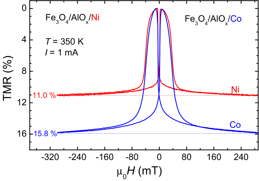
In the following, we obtain TMR values of magnetite-based MTJs with different counter electrodes (Ni and Co) and we estimate the spin polarization of the Fe3O4 electrode. As shown in Fig. 4, MTJs with rectangular shape having the same Fe3O4 base electrode and same AlOx tunneling barrier, but a Ni or Co counter electrode, show a maximum TMR effect of 11% for Ni and 15.8% for Co at 350 K. A different sample with an improved ring-shaped geometry revealed a maximum TMR effect of 20% at room temperature and 27% at 350 K for Co (not shown here). To our knowledge, the latter value is larger than the highest TMR effects reported so far for Fe3O4 based MTJs at or above room temperature (cf. Table 1). Using the simple Julliére model [63], the measured TMR values can be related to the spin polarizations and of the ferromagnetic electrodes according to
| (2) |
With the literature values and [64], we derive a spin polarization for magnetite at room temperature between (Ni) and (Co). However, this value is by far too low as compared to recent data () obtained by spin-resolved photoelectron spectroscopy [72, 73]. We attribute this to spin-flip scattering at defect states in the tunneling barrier or inelastic tunneling processes involving magnon scattering. For example, if a finite amount of the tunneling current is involving spin-flip processes, it has been shown that the ideal TMR value of eq.(2) is reduced to [90, 91]
| (3) |
Here, is the part of the tunneling current involving spin-flip processes and is the total tunneling current in the antiparallel magnetization configuration. There may be various sources of such as inelastic tunneling via defect states in the barrier or tunneling processes involving magnon scattering in the junction electrodes. It is immediately evident that a finite value of is causing a reduction of the measured TMR effect. The strong temperature dependence of the tunneling resistance of our junctions (cf. Fig. 3) shows that there is a large amount of inelastic tunneling current. This is consistent with the small absolute TMR⋆ values of up to 27% measured for our investigated MTJs.
The determination of the sign of cannot be done unambiguously by evaluating the TMR effect in magnetic tunnel junctions as it depends on the sign of of the counter electrode. From theory, is predicted and observed for Ni in spin-polarized scanning tunneling microscopy experiments [92], but not in electrical transport at AlOx interfaces [64]. From eq. (2), leads to a negative spin polarization for Fe3O4 as discussed above and reported by spin-resolved photoelectron spectroscopy [72, 73], even through an AlOx barrier [93]. However, assuming results in a positive value for and is reported for transport across the AlOx interface by the same authors [93].
2.4 Giant TMR Effect by Current Redistribution.
A detailed study of MTJs with different shape of the junction area showed that for specific samples the TMR values derived according to eq. (1) can become huge, change sign, and depend sensitively on temperature. This effect could be reproduced in several samples. However, the temperature regime in which this effect occurs strongly depends on the geometry and the layer structure of the MTJs. To illustrate this effect, in Fig. 5 we show curves of a ring-shaped MTJ based on a TiN(35 nm)/Fe3O4(20 nm)/AlOx (3 nm)/Co(15 nm) stack at different temperatures around K. The resistance is obtained by simply dividing the measured voltage drop across the MTJ by the applied current of . Obviously, the curves are shifted to smaller values with increasing temperature. Most interestingly, for parallel magnetization of the ferromagnetic layers, i.e. for applied fields well above the coercive fields of the electrode materials, the curve is close to zero and even becomes negative with increasing temperature. Here, negative means that the measured voltage drop across the junction has become negative. If we use the curves of Fig. 5 to formally derive a TMR value according to eq. (1), we obtain giant values of several 1000%, since we divide by a very small value. Furthermore, the derived TMR value can change sign due to the sign change of . We note, however, that the overall difference between the anti-parallel and the parallel magnetization configuration of the MTJ does not change significantly.
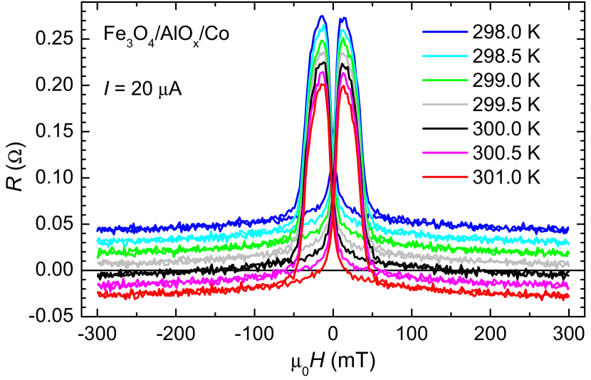
We attribute the effect described above to the specific choice of the junction geometry and layer structure. By a proper choice of parameters a significant redistribution of the current in the junction electrodes is achieved. A similar effect has been reported earlier [94] for junctions with very large area and small thickness of the junction electrodes. When using very thin or highly resistive junction electrodes, the voltage drop along the junction electrodes can become comparable to the voltage drop across the tunneling barrier. To derive the TMR value, only the voltage drop across the tunneling barrier is required. However, in the real experimental situation both this voltage drop and part of the voltage drop along the junction electrodes is measured. In this case, the determination of the TMR value is difficult and a naive analysis can lead to giant, geometry-induced TMR effects as discussed above. Whereas for junctions with metallic electrodes this effect only appears for MTJs with very large junction area and thin electrodes, in our MTJs this effect can be reproducibly obtained also for small junction dimensions in the micrometer range and therefore may be interesting for applications. This is caused by the much higher resistivity of the base electrode of our MTJs.
To confirm the scenario discussed above, we calculated the spatial distribution of the electrical potential and the current in ring-shaped MTJs using finite element method (FEM) simulations. The geometry of the ring-shaped junctions is shown in Fig. 6. The in-plane conductivities used in the simulations for the various layers of the junction stack are summarized in Table 3. Since the simulation tool did not allow to represent the real dimensions of the sample because of its large aspect ratio we scaled the geometry and the conductivity in the out-of-plane direction by a factor of 100. Fig. 6 shows the calculated electrical potential distribution in the MTJ. The current is driven from the lower left to the upper right by a fixed source voltage of 50 mV. The voltage drop across the MTJ is measured between the lower right () and the upper left ().
| material | conductivity |
|---|---|
| bottom electrode, rectangular (TiN) | |
| bottom ferromagnet, ring (Fe3O4) | |
| tunneling barrier, ring | |
| top ferromagnet, ring (Co) | |
| wiring layer, rectangular (Au) |
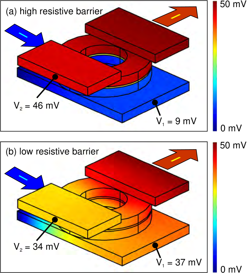
Figure 6(a) shows the simulation result for a highly resistive barrier (). The conductivity of the tunneling barrier is lower by more than two orders of magnitude as compared to the conductivities of all other layers. This is the usual situation present in most MTJs with high conductivity metal electrodes. The color-coded representation of the potential distribution immediately shows that in this case almost the whole voltage drop occurs across the barrier, whereas the potential distribution in the bottom electrode (blue) and the top electrode (red) is homogeneous. From the simulation we obtain mV and mV, resulting in a voltage drop mV between the voltage probes. Fig.6(b) shows the simulation result for a tunneling barrier with higher conductivity (). Now the conductivity of the tunneling barrier is of the same order as the conductivity of the bottom electrode. In this case a completely different potential distribution is obtained. Only a minor part of the voltage drop occurs across the barrier and an inhomogeneous potential distribution is obtained within the junction area. The calculated potentials at the position of the voltage probes are mV and mV, resulting in a negative voltage drop of mV between the voltage probes. This result even holds when increasing the width and length of the bottom electrode. The FEM simulations clearly show that the measured voltage drop can become very small and even negative if the total resistance of the tunneling barrier becomes smaller than the total resistance of the electrode material in the junction area. For our MTJs this is the case due to the low conductivity of the bottom electrode. For MTJs with high conductivity metal electrode, this is the case only for very large junction area and/or very thin junction electrodes.
We note that an equivalent effect is known for Josephson junctions in the normal state, if the current leads have resistivities of the same order as the insulating barrier. For a structure where the top and bottom electrodes are parallel and separated by a rectangular insulating barrier, Pedersen et al. developed a one-dimensional model [95]. For MTJs with a so-called cross-strip geometry where the top and bottom electrodes are aligned perpendicular to each other, the current distribution was investigated using two-dimensional FEM simulations by van de Veerdonk et al. [96]. They showed that an inhomogeneous current distribution across tunnel junctions can suppress the measured voltage drop which may result in a divergence of the determined TMR value. This is in good agreement with the results of our three-dimensional FEM simulations describing the more complex geometry of our MTJs. We note that our simulations have been performed as proof of principle and are not intended to reproduce all details of the real junctions.
2.5 Fully Epitaxial MTJs: The Case of the MgO Barrier.
According to the high spin polarization of magnetite, very high TMR values are expected for MTJs consisting of two Fe3O4 electrodes. Therefore, we have grown fully epitaxial TiN/Fe3O4/MgO/Fe3O4/Co/Au stacks on (001) oriented MgO substrates as described in 2.1. A thin Co layer on top of the ferromagnetic Fe3O4 counter electrode was introduced to modify the coercive field of the counter electrode. In this way different coercive fields of the bottom and top electrode could be achieved, allowing for the realization of the antiparallel magnetization configuration. However, the magnetic characterization of the stacks showed a magnetic coupling of the two ferromagnetic electrodes at temperatures below 250 K. As already discussed in 2.2, this coupling results in a synchronous switching of the magnetization in the two electrodes despite the different coercivities. Therefore, a stable antiparallel magnetization configuration of the two electrodes cannot be achieved. There are different scenarios for the origin of the coupling. A simple origin of ferromagnetic coupling are pinholes in the barrier layer. However, the TEM analysis of the MTJs showed that the MgO barriers are homogeneous and pinholes in the typically 5 nm thick barrier layer are unlikely. Another possibility are Fe impurities and a large density of defect states within the MgO barrier which mediate a ferromagnetic coupling at low temperatures. The impurities may stem from the high energy Fe ions in the plasma plume, impinging on the barrier layer during the deposition of the Fe3O4 counter electrode thereby causing intermixing. To clarify this issue, a combined transmission electron microscopy (TEM) and electron energy-loss spectroscopy (EELS) investigation was performed.
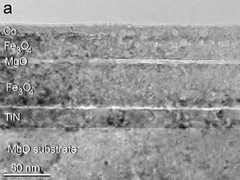
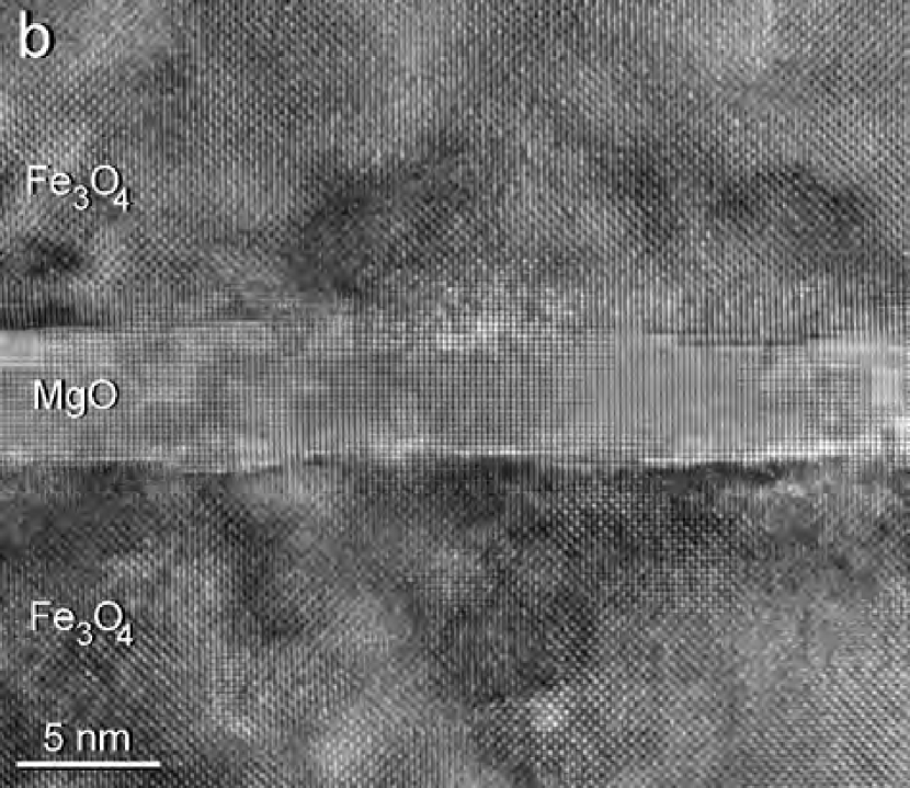
A TEM micrograph of the MTJ stack in cross-section is shown in Fig. 7(a). The layers of the stack were measured to 21 nm (TiN), 55 nm (Fe3O4), 5 nm (MgO), 22 nm (Fe3O4), and 8 nm (Co). The thin isolating MgO barrier layer as well as the Fe3O4 electrodes can be seen to be grown homogeneously with constant thickness. The HR-TEM image in Fig. 7(b) shows that the MgO barrier exhibits some thickness variations which are the result of steps and ledges at the two interfaces between MgO and the adjacent Fe3O4 layers. Nevertheless, at some positions without steps a clear interface can be observed at the two oxides proving an atomically sharp transition from Fe3O4 spinel to MgO. The continuation of the (200) lattice planes of MgO and the (400) planes of Fe3O4, running vertically, prove perfect epitaxy between the lower magnetite layer across the MgO barrier to the upper magnetite layer. This observation definitely proves the continuation of the oxygen sub-lattices in the three oxide layers.
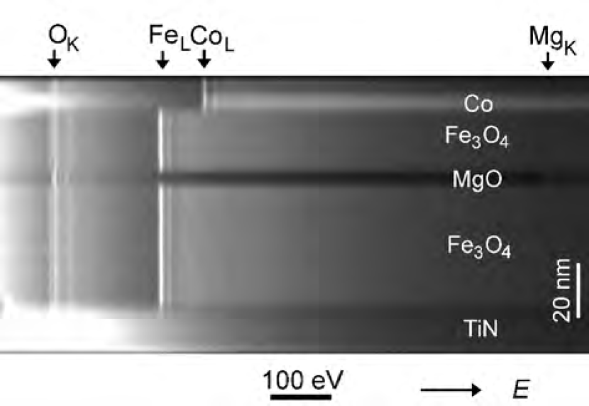
To investigate the chemical composition of the MgO tunneling barrier, EELS was applied with an electron probe of less than 1 nm in diameter. The beam was scanned with 1 nm increment across the layer stack, and EEL spectra were acquired simultaneously at any beam position. This technique, named energy-loss spectroscopic profiling (ELSP) [97, 98], results in spectroscopic images with EELS intensity as a function of energy loss and the spatial co-ordinate of the electron beam line profile as shown in Fig. 8. In the energy loss range shown the spectrum image contains the edges of Co and Fe where the MgO barrier causes the gap in the Fe- EELS signal. The Mg- edge is at eV and is thus of low intensity. The oxygen- edge reveals the difference in near-edge structure of the MgO and magnetite layers, respectively, which is the result of the different chemical neighbors of oxygen and of the differing co-ordination.
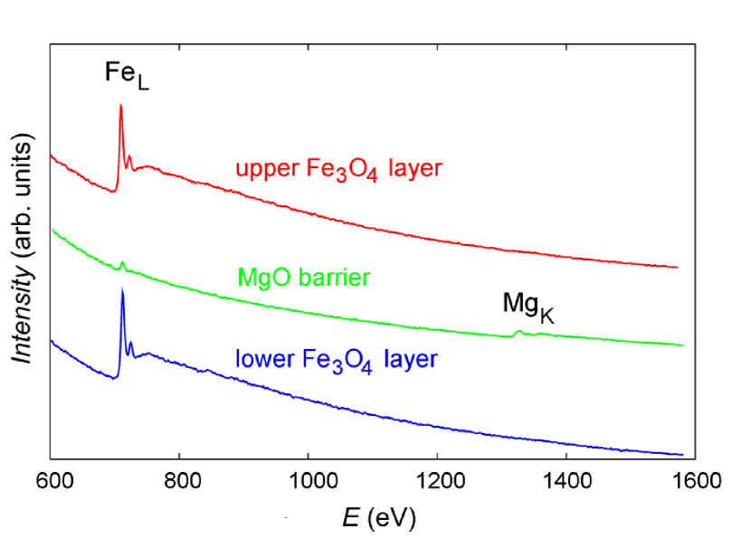
To obtain unambiguous information on the chemical composition of the MgO barrier layer, the EEL spectrum in the center of the MgO barrier was analyzed and is displayed in Fig. 9 together with spectra of the two magnetite layers. In this spectrum a faint signal at the energy loss of the Fe- edge (708 eV) is present besides the Mg- edge proving a small amount of iron in the MgO barrier. The obvious question arising at this point is whether or not iron-doped MgO is a dilute magnetic semiconductor. If this is the case, the observed ferromagnetic coupling across the MgO barrier is easy to understand. To clarify this point, we have grown Fe-doped epitaxial MgO films by PLD using an iron-containing MgO target. However, the magnetization of these films was below the noise level of the SQUID magnetometer.
2.6 Summary.
We have successfully fabricated Fe3O4-based MTJs with different size and shape of the junction area. For MTJs with AlOx barriers a separated switching of the magnetization of the two ferromagnetic electrodes is obtained. These junctions show a reproducible TMR effect with an ideal symmetric switching behavior. The TMR effect could be observed in the whole investigated temperature range from 150 K to 350 K. At 350 K, TMR values up to 27% were obtained. A giant geometry-induced TMR effect can be generated in Fe3O4-based MTJs due to the high resistivity of the electrode material. Our data suggest that Fe3O4 with its high spin polarization and high Curie temperature is interesting for spintronic devices. However, to access the full potential of this material, the quality of suitable tunneling barriers and involved interface layers has to be improved.
3 Ferromagnetic Semiconductors.
The rapidly evolving field of spintronics requires material systems combining ferromagnetism (FM) with the versatile electronic properties of semiconductors. Therefore, the integration of semiconducting and magnetic properties in one and the same material to realize magnetic semiconductors was attracting broad attention. Dilute magnetic semiconductors (DMS) such as the widely studied material (Ga,Mn)As are attractive in this regard. Unfortunately, this well established DMS has a Curie temperature K [10], preventing room temperature applications. In contrast, K has been predicted for the oxide semiconductor ZnO on partial substitution of Zn by a magnetic transition metal such as Mn or Co [11]. Indeed, ferromagnetic behavior has been observed in Zn0.95Co0.05O thin films at room temperature [12]. Some authors even report on two magnetic regimes depending on the charge carrier density [99], or on gate-control of magnetism [100]. However, there is an ongoing debate on the nature of the ferromagnetic behavior in oxide semiconductors [59, 101, 102] as the observed behavior might also be traced back to nanometer-sized precipitates of the Co dopant atoms embedded in a nonmagnetic ZnO matrix. The same controversy holds for Mn in Ge [103, 104].
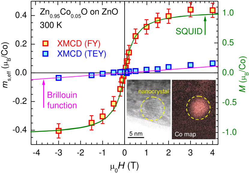
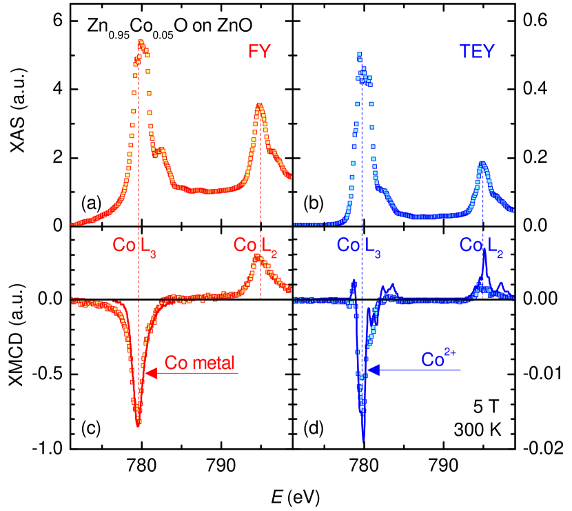
To unambiguously clarify the nature of magnetism in Zn0.95Co0.05O, we prepared thin films using laser-MBE and carefully investigated their structural and magnetic properties as discussed in detail in [59]. In particular, we have combined SQUID magnetometry, X-ray magnetic circular dichroism (XMCD), and AC susceptibility measurements with careful X-ray and high resolution TEM studies. We simultaneously recorded XMCD spectra in both the total electron (TEY) and the fluorescence yield (FY) modes, allowing for an element-specific distinction between surface and bulk magnetic properties, respectively (Fig. 10). Our data provide clear evidence that our Zn0.95Co0.05O thin films are not homogeneous DMS. The large magnetic moments observed at room temperature in some of the samples could rather be traced back to the presence of nanometer-sized superparamagnetic Co precipitates within the bulk of Zn0.95Co0.05O, which were directly evidenced by XMCD and energy-filtering transmission electron microscopy (EF-TEM) (Fig. 11). Other samples show pure paramagnetism of isolated Co2+ moments from room temperature down to 5 K. More details have been published elsewhere [59, 102]. Similar behavior has been reported for other dilute magnetic systems, like GaN:Gd [107]. Of course, our data do not prove that the realization of a DMS is impossible for ZnO:Co. However, more effort is required to unambiguously determine the nature of ferromagnetism, and conclusions based on superficial studies only presenting “hysteresis” curves should be considered with care.
Since the room temperature realization of ferromagnetic and semiconducting properties in one material may turn out difficult, the use of ferromagnet/semiconductor heterostructures may be the appropriate solution. Here, the use of oxide materials may be advantageous. We recently have shown that semiconducting ZnO can be grown epitaxially on ferromagnetic Fe3O4 and vice versa [51]. Such oxide heterostructures are interesting since the semiconducting and ferromagnetic oxide have similar resistivity, avoiding the well-known resistivity mismatch problem at ferromagnetic metal/semiconductor interfaces [108] regarding efficient spin injection. Future studies have to show whether the interfaces in the oxide heterostructures can be controlled and engineered in an adequate way to allow for the realization of spin injection devices.
4 Multiferroics and Strain Effects.
An active and promising field of research is the integration of different ferroic ordering phenomena such as ferromagnetism, ferroelectricity, or ferroelasticity in one and the same material [9, 109, 110]. The coexistence of ferroelectricity and ferromagnetism in novel multi-functional materials is particularly interesting, since this could allow the realization of new functionalities of electro-magnetic devices, such as the electric field-control of magnetization. Unfortunately, it turned out that there are very few intrinsic ferroelectric/ferromagnetic multiferroics because the standard microscopic mechanisms driving ferroelectricity and ferromagnetism are incompatible. They usually require empty and partially filled transition metal orbitals, respectively [111]. Furthermore, most of the multiferroics reported so far are antiferromagnets, which are not expected to respond noticeably when applying magnetic fields. This has initiated the search for other mechanisms favoring the coexistence of ferroelectricity and magnetic order as, for example, in BiMnO3 [112] or in extrinsic, two-component multiferroic thin film heterostructures [8]. For the realization of useful multiferroic materials, however, the different ferroic order parameters do not only have to coexist, but must be coupled to each other (Fig. 12) to enable, e.g. an electric field control of the magnetization in magnetoelectric multiferroics.
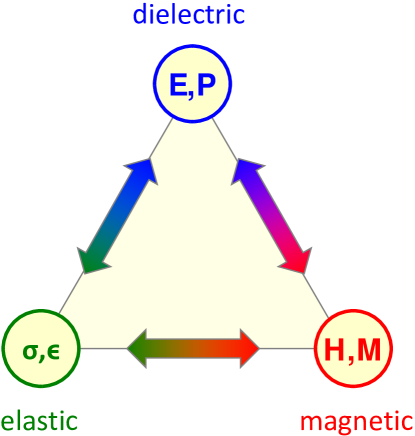
Here, we report on different oxide systems which are promising in this regard. We first study the dielectric and magnetic properties of the perovskites BiFeO3 and BiCrO3 which are considered as intrinsic multiferroic materials and search for a magnetoelectric coupling in these materials. Second, we focus on hybrid systems consisting of ferroelectric and ferromagnetic materials. As an example, we discuss the behavior of multiferroic hybrids consisting of epitaxial thin films of the ferromagnet Sr2CrReO6 grown on ferroelectric BaTiO3 substrates.
4.1 Intrinsic Multiferroics: BiFeO3 and BiCrO3.
The perovskite BiFeO3 is one of the few robust materials with ferroelectric and antiferromagnetic order well above room temperature. In bulk material, BiFeO3 is antiferromagnetic below the Néel temperature of K and ferroelectric below K [113, 114]. Thin films of BiFeO3 are discussed for application as exchange biasing ferromagnetic layers in spintronic multilayer structures [115, 116, 117, 118]. Strained thin films of BiFeO3 have attracted renewed interest after the report of a high ferroelectric polarization of together with a high residual magnetic moment of per formula unit (f.u.) [119]. However, there is an ongoing controversial discussion about the origin of this saturation magnetization [120, 121] as the initially reported magnetization values in relaxed BiFeO3 thin films could not be reproduced by subsequent work [60, 120, 122, 123]. In our work we found /f.u. in strained BiFeO3 thin films [60] which is in full agreement with other recent publications [120, 122, 123] and density functional calculations [124]. Moreover, it was shown that strain-free bulk crystals of BiFeO3 do not show any parasitic ferromagnetism down to 2 K at all [125]. Whether or not the small magnetic moments reported for BiFeO3 thin films and also observed in our samples originate from nanoscale metallic Fe precipitates or spin canting has to be clarified. Details on the growth as well as the structural and magnetic characterization of our BiFeO3 thin films can be found in [60].
Another interesting candidate for an intrinsic multiferroic material is BiCrO3. Bulk BiCrO3 is antiferromagnetic below K [126] and shows a weak ferromagnetic moment, which is attributed to Cr3+ spin canting [60]. The situation is similar in thin films, where a Néel temperature between 120 K [127] and 140 K [128] is reported. Regarding dielectric properties, the picture is still unclear as both ferroelectricity at room temperature [127] and antiferroelectricity at 5 K [128] have been observed. In the following we present results on the fabrication and characterization of this material.
Thin Film Deposition.
We have grown -axis oriented epitaxial BiCrO3 thin films by laser-MBE with in-situ RHEED [13, 15] on (001)-oriented SrTiO3 substrates. The PLD process was performed in the same way as described in subsection 2.1 for Fe3O4. We used polycrystalline targets with excess bismuth in the composition Bi1+δCrO3 (). The growth parameters were optimized with regard to the structural quality of the samples. The thin films were grown by imposed layer-by-layer interval deposition in O2 atmosphere at a pressure of mbar and a substrate temperature of C with a laser fluence of 2 J/cm2 at the target [60]. To enable a dielectric characterization of the samples in spite of the insulating SrTiO3 substrate, some thin films have been deposited with an underlying bottom electrode layer of the conducting oxide SrRuO3 ( at 300 K) with a thickness between 10 nm and 20 nm. The SrRuO3 film was also grown by PLD from a stoichiometric target in O2 atmosphere (0.15 mbar) at a substrate temperature of C.
Structural Characterization.
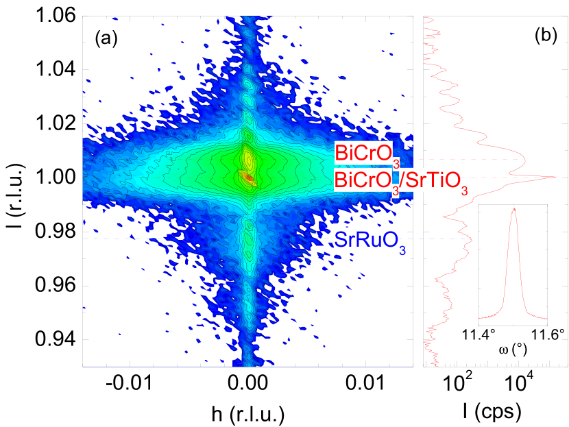
The structural properties of the films were investigated by X-ray diffraction using Cu K radiation and a high-resolution four-circle diffractometer (Bruker AXS discover). Fig. 13(a) shows a reciprocal space map around the (001) reflection of the SrTiO3 substrate obtained at room temperature. A line scan for (-scan) is shown in Fig. 13(b). The film thicknesses are 19 nm (SrRuO3) and 65 nm (BiCrO3). BiCrO3 shows two reflections at and , as indicated by the broad green regions in (a). The reflection from SrRuO3 is located at . Satellites due to Laue oscillations from the BiCrO3 as well as the SrRuO3 reflections are visible, demonstrating that the films are coherently strained and have small surface and interface roughnesses. Moreover, the rocking curve of the BiCrO reflection displays a small full width at half maximum of [inset in Fig. 13(b)] demonstrating a very low mosaic spread.
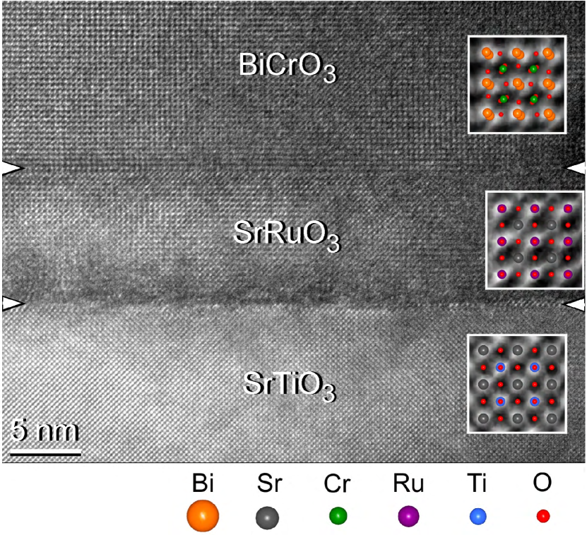
The high structural quality of the BiCrO3 layer as well as of the SrRuO3 electrode layer is demonstrated in real space at high spatial resolution by TEM studies (Fig. 14). First the thicknesses of the two layers were measured from TEM images to 10 nm (SrRuO3) and 28 nm (BiCrO3) in this sample. The crystals containing the interfaces SrTiO3/SrRuO3 and BiCrO3/SrRuO3 are imaged in the HR-TEM micrograph (Fig. 14). It is worth noting that the image contrast in the three crystals, all with O3 perovskite structure, is different. This is the result of the metal ions and which have very different scattering power in the three crystals, and the scattering potential scales with the atomic number . In SrTiO3, the scattering powers of Sr () and of the Ti+O column () are similar, and therefore the type of lattice planes dominate the crystal lattice contrast, forming a square pattern rotated to the axis. In SrRuO3, the site atom ruthenium has the highest scattering potential and the atomic columns Ru+O () dominate the contrast and produce a square array of lattice planes centered at the sites. In BiCrO3, the heavy metal bismuth on the site is by far the strongest scatterer () and produces again a square array contrast of lattice planes, here, however, centered at the sites. Close inspection of the lattice plane image (Fig. 14) reveals indeed a shift of the dot contrast from SrRuO3 to BiCrO3 of half the axis parallel to the interface. To better illustrate the contrast in the perovskite crystals and the position of the atomic columns, insets at high magnification are placed into Fig. 14. These observations prove continuation of the oxygen sub-lattices of the three perovskite crystals across the interfaces. A further detail concerning the interfaces is worth noting: the interface SrTiO3/SrRuO3 appears not to be atomically abrupt. This is very likely the result of surface treatment of the SrTiO3(001) crystal by grinding and polishing. Nevertheless, the SrRuO3 electrode has grown epitaxial, and even more impressive is the interface between the BiCrO3 and SrRuO3 layers which appears atomically planar, i.e. without steps, and with a direct structural transition from one phase to the other. In summary, the observations and structural characterization by X-ray diffraction and TEM prove that the thin film system of BiCrO3 and SrRuO3 is state-of-the-art grown with outstanding quality of the crystals.
Magnetic Characterization.
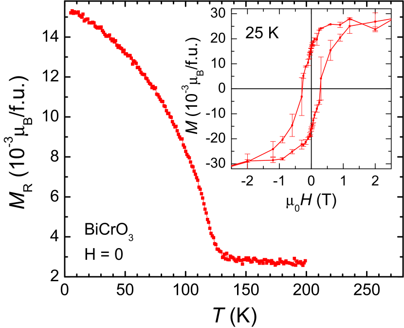
Magnetization measurements were performed with a SQUID magnetometer in magnetic fields up to T applied in the film plane. Fig. 15 displays the remanent magnetization , measured after field cooling at 7 T on increasing temperature in zero field. Although antiferromagnetic, the sample shows a weak residual remanent magnetization of /f.u. at low temperatures. We note that this observed parasitic ferromagnetism sets in below a critical temperature of about K. This value is slightly larger than the Néel temperature of bulk material ( K [126]) and than the values for parasitic ferromagnetic ordering reported in literature [127, 129]. This may be related to the small tensile strain in our BiCrO3 films. A magnetic field-loop recorded at 25 K demonstrates that saturates at about /f.u. for fields higher than 2 T (see inset of Fig. 15). The coercivity of this parasitic ferromagnetism is larger than for our BiFeO3 films [60]. The scatter seen in the data is caused by the small sample volume leading to absolute values of close to the resolution limit of the SQUID magnetometer ( Am2). In summary, the observed magnetic properties of our BiCrO3 films are consistent with the picture that the Cr3+ spins are coupled antiferromagnetically and that a slight canting of the spins results in a weak ferromagnetic signal [124, 130].
Dielectric Characterization.
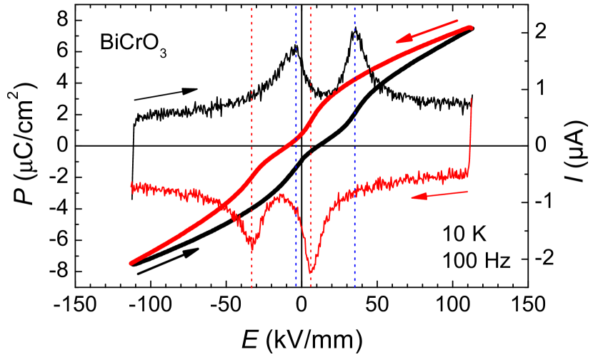
The dielectric properties of the thin film samples were investigated using a commercial ferroelectric tester (aixACCT TF analyzer 2000). Figure 16 displays the electric loop from a 177 nm thin film of BiCrO3 together with the dielectric current, recorded in dynamic mode at 100 Hz at a temperature of 10 K in electric fields of up to kV/mm (corresponding to a voltage of 25 V) applied across the BiCrO3 layer. The curve shows an antiferroelectric hysteresis loop with an electric polarization close to at high electric fields. Two “humps” per field sweep direction at kV/mm and kV/mm are visible in the loop. These observations clearly point to the presence of anti-ferroelectric ordering in this material which becomes more obvious when investigating the dielectric current . This quantity shows two clear and well pronounced maxima per field sweep direction at the same values where the “humps” in are observed. We interpret this double peak feature as evidence for the switching of two ferroelectric sub-polarizations in a dipole lattice.
Summary.
Neither BiFeO3 nor BiCrO3 shows the expected coexistence of ferromagnetism and ferroelectricity. (i) BiFeO3 is antiferromagnetic. The existence of the reported parasitic ferromagnetic phase with moments up to /f.u. [119] could not be reproduced and most likely is an artefact caused by metallic Fe precipitates in the BiFeO3 thin films. (ii) BiCrO3 is antiferroelectric on large scales instead of showing ferroelectric behavior. (iii) Neither for BiFeO3 nor BiCrO3, we were able to find any indication for intrinsic magnetoelectric coupling.
4.2 Extrinsic Multiferroics: Piezo-strain in Fe3O4.
Another promising approach to realize multiferroic coupling is the fabrication of heterostructures composed of materials with different ferroic properties. Of course, in such multilayers coexisting ferroic ordering phenomena can be easily realized. The key task here is to establish a coupling of the order parameters at the interfaces between the ferroic sublayers. Along this line, the use of strain to establish a finite coupling via the elastic channel (see Fig. 12) is promising. We showed in [27, 28] that the magnetic anisotropy and in turn the magnetization direction of a ferromagnetic layer can be varied by an electric field making use of the elastic channel. In our experiments we used magnetite (Fe3O4) as a prototype ferromagnet. Epitaxial Fe3O4 was deposited by laser-MBE with in-situ RHEED [13, 15] on (001)-oriented MgO substrates as described in 2.1. The thin films with a thickness of 44 nm were grown in an inert Ar atmosphere at a pressure of mbar with a laser fluence of 2.5 J/cm2 at the target and a substrate temperature of C. After deposition, the MgO substrate was polished down to a thickness of about . To introduce an in-situ tunable strain, we cement a commercial Pb(Zr,Ti)O3 piezoelectric actuator on top of the Fe3O4 thin film [131, 132]. The expansion (or contraction) of the piezoelectric actuator as a function of the applied electric voltage is directly transferred into the magnetite film, yielding a voltage-controllable strain contribution. To optimize the induced strain, we cement the piezoactuator face to face onto the Fe3O4 thin film. The induced strain was determined by X-ray diffraction via the changes of the lattice parameters of the underlying MgO substrate [28].
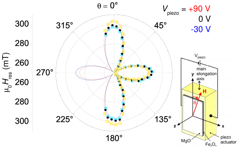
To determine the magnetic anisotropy, we performed ferromagnetic resonance (FMR) spectroscopy in the X-band (microwave frequency of 9.3 GHz) at room temperature. The angular dependence of the resonance field for different values for was successfully modeled using magnetoelastic theory (Fig. 17) [28]. Implying a strain transmission efficiency factor of 70% from the piezoactuator to the Fe3O4 thin film, we find excellent agreement with experiment. The changes of magnetic anisotropy induced by this piezo-strain make it possible to shift the minimum of the free energy and thus the magnetization orientation by about within the Fe3O4 film plane. As the magnetostriction constant [133] is comparable to those of e.g. Fe, Ni, or CrO2 [134, 135], our results show that a piezo-strain control of the magnetization orientation is a realistic and versatile scheme applicable to a variety of ferromagnets [27, 28, 29].
4.3 Extrinsic Multiferroics: Sr2CrReO6 on BaTiO3.
Even higher strains are possible when replacing the piezoelectric actuator by a ferroelectric substrate. This integration of ferromagnetic (FM) and ferroelectric (FE) degrees of freedom in epitaxial hybrid heterostructures is promising for the realization of multi-functional material systems with improved or novel functionality. As an example, we exploited the strain-induced change of the magnetic coercivity of polycrystalline Ni in a FM/FE hybrid and demonstrated both reversible and irreversible magnetization control [136]. Here, we will focus on an epitaxial all-oxide FM/FE system.
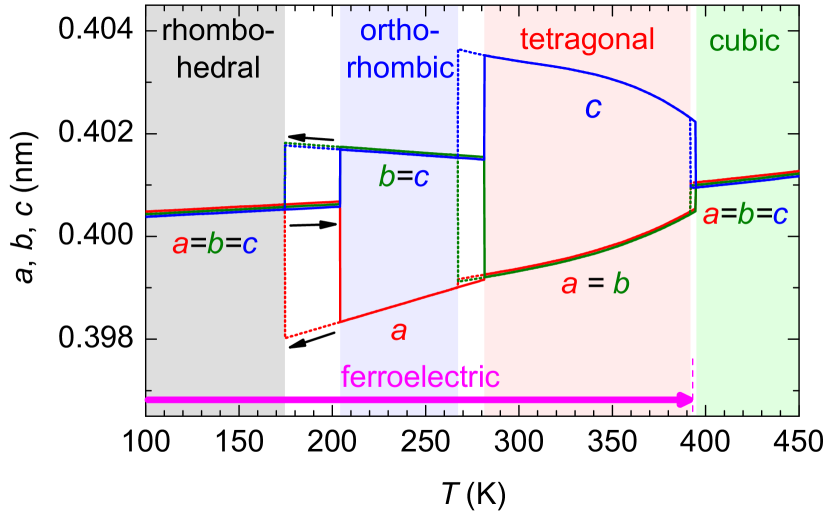
Barium titanate (BaTiO3) is the prototype ferroelectric. Its crystallographic structure shows a variety of phase transitions, dependent on the temperature (see Fig. 18) [137]. Above 393 K, bulk BaTiO3 is cubic and paraelectric. Below 393 K, it becomes ferroelectric and its lattice structure changes to tetragonal. Within the ferroelectric state, the lattice symmetry is further reduced to orthorhombic (below 278 K), and finally to rhombohedral (below 183 K). The dielectric constant, the spontaneous polarization, as well as the lattice constants change abruptly at these phase transition temperatures, accompanied by a thermal hysteresis [138]. Recently, there have been reports on CoFe2O4/BaTiO3, SrRuO3/BaTiO3, La0.67Sr0.33MnO3/BaTiO3, and Fe3O4/BaTiO3 hybrids [139, 140, 141, 142, 143, 144]. They show a magnetoelectric coupling effect, manifesting itself as a change in the magnetization and resistance of the ferromagnetic thin film at the structural phase transition temperatures of BaTiO3. In this regard, another promising material is the ferromagnetic double perovskite Sr2CrReO6 which is known for a giant anisotropic magnetostriction [145] caused by a large orbital moment on the Re site [53]. In addition, it has a high Curie temperature of 635 K [146] well above room temperature, and a predicted high spin polarization of 86% [147]. We recently have shown that ferromagnetic Sr2CrReO6 grown epitaxially as a thin film on BaTiO3 substrate exhibits qualitative changes in its magnetic anisotropy at the BaTiO3 phase transition temperatures [148]. Abrupt changes in the coercive field of up to 1.2 T along with resistance changes of up to 6.5% have been observed [148]. Here, we will discuss the structural properties of the samples.
Thin Film Deposition.
Epitaxial Sr2CrReO6 thin films were deposited by laser-MBE with in-situ RHEED [13, 15] on (001)-oriented BaTiO3 substrates. The thin films with a thickness of approx. 80 nm were grown in O2 atmosphere at a pressure of mbar with a laser fluence of 2 J/cm2 at the target and a substrate temperature of C (i.e. in the cubic, paraelectric phase of BaTiO3). These parameters were found to be optimal for the growth of Sr2CrReO6 films on SrTiO3 substrates [149] and also are appropriate for the growth on BaTiO3 substrates. After film deposition, the sample is slowly cooled down to room temperature with the substrate undergoing a phase transition to the tetragonal and ferroelectric phase. As there is no preferential direction for the electric polarization, however, the ferroelectric state will decompose into many different ferroelectric domains as evidenced by X-ray diffraction [148].
Structural Characterization.
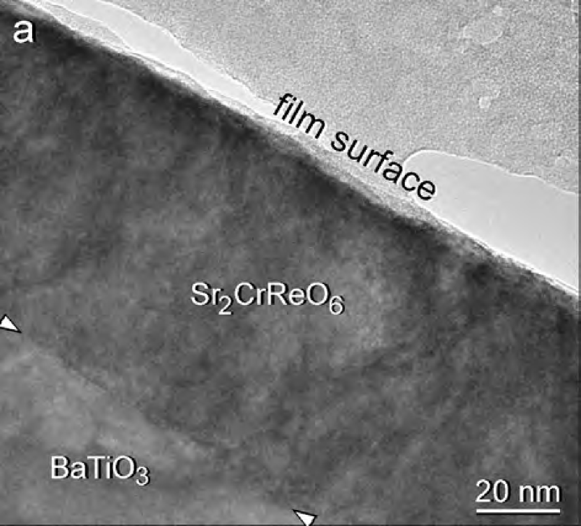
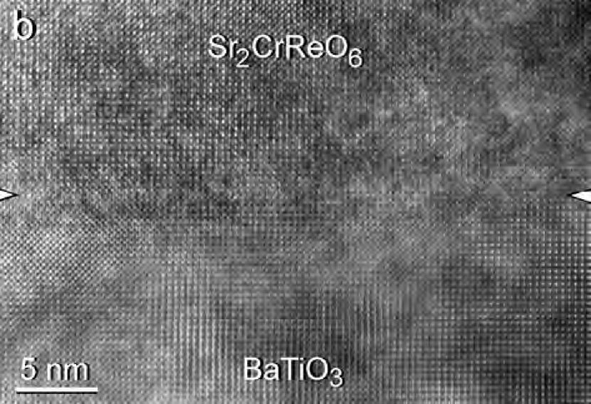
High-resolution TEM studies were performed at thin cross-sections of the Sr2CrReO6 films on BaTiO3 prepared by standard specimen preparation techniques. Fig. 19(a) shows a thin film with ca. 81 nm thickness. Electron diffraction reveals (i) a perfect epitaxial orientation relationship between the double perovskite film and BaTiO3 and (ii) a large single domain of the tetragonal substrate. However, the difference between the and lattice parameter of tetragonal BaTiO3 as well as the cell parameter differences in the strained Sr2CrReO6 film (see Fig. 19) are ca. 1% and are thus too small to be measured by electron diffraction. The HR-TEM micrograph (Fig. 19(b)) is of the interface region which appears without any voids or other defects. The lattice mismatch between of Sr2CrReO6 and of BaTiO3 can be estimated to ca. 2% (Fig. 19), however misfit dislocations were not observed regularly. The lattice image contrast in the Sr2CrReO6 film is clearly dominated by the columns () vs. the Sr columns () while in BaTiO3 the barium columns () predominantly cause the image contrast. In both crystals, a square array of dots is produced with spacing of or of BaTiO3 and the spacing of or of Sr2CrReO6, respectively. Close inspection of the image contrast reveals a gradual shift of the square dot array along the interface from BaTiO3 to Sr2CrReO6 by half of the square length showing the continuation of the site and site positions and hence proving an undisturbed transition of the oxygen sub-lattices of the two perovskite-type crystals across the interface.
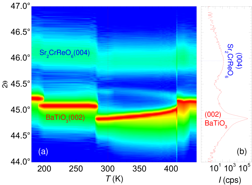
High-resolution X-ray diffraction was performed using Cu K radiation and a high-resolution four-circle diffractometer (Bruker AXS discover). Fig. 20 shows -()-scans from the same sample as in Fig. 19 for different temperatures between 180 K and 450 K. The (004) reflection from the Sr2CrReO6 thin film and the (002) reflection from the BaTiO3 substrate can be clearly distinguished. It is obvious that the angles of both reflections change abruptly when the BaTiO3 undergoes structural phase transitions. The line scan at 300 K (Fig. 20(b)) reveals no crystalline parasitic phases in the thin film. A more detailed picture is obtained from reciprocal space maps showing that the reflection from the BaTiO3 substrate is split due to the presence of different ferroelectric domains in the tetragonal phase ( domains: BaTiO3(200/020) and domains: BaTiO3(002)) [149]. From the intensity ratio of the Sr2CrReO6(101) and (404) reflections (not shown here) the amount of Cr/Re disorder is estimated to be less than 30%, i.e. less than 30% of the Cr3+ ions are on Re5+ sites and vice versa [148].
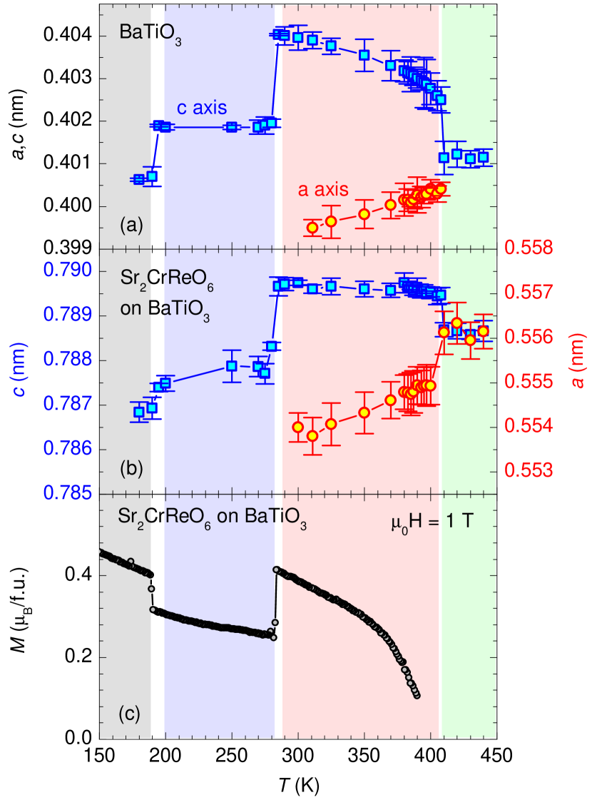
From the observed angles, we calculate the and lattice parameters for both the substrate and the thin film. The results are displayed in Fig. 21(a,b). All data were obtained with decreasing temperature. The axis lattice parameter of our BaTiO3 substrate (Fig. 21(a)) nicely follows the behavior reported for bulk material (see Fig.18) [137]. It is slightly above nm in the cubic phase, then increases to nm (tetragonal), drops to nm (orthorhombic), and finally becomes nm (rhombohedral). Also the parameter behaves as expected in the tetragonal phase. For the Sr2CrReO6 thin film (Fig. 21(b)), the axis parameter shows the same temperature dependence as for the substrate. This confirms coherent growth and biaxial strain transfer from BaTiO3 into the epitaxial film. Also the lattice parameter follows the trend of the substrate. In the tetragonal phase, however, it does not display any temperature dependence, in contrast to the behavior of BaTiO3. In summary, the structural analysis shows that the lattice parameters of the Sr2CrReO6 thin film change abruptly at the BaTiO3 phase transition temperatures.
Magnetic Characterization.
The magnetic properties were determined by a SQUID magnetometer with a magnetic field of 1 T applied in the film plane (Fig. 21(c)). At the BaTiO3 phase transitions, we observe abrupt changes of the magnetization , which drops at the tetragonal-orthorhombic transition and increases again when entering the rhombohedral phase. We note that we observe a small thermal hysteresis due to the first order structural phase transition of the substrate. A careful investigation [148] shows that the values for saturation magnetization, remanent magnetization, and coercivity clearly differ from each other for the different structural phases of the substrate. Therefore, we attribute the observed discontinuities to a change of the magnetic anisotropy of the thin Sr2CrReO6 layer. They are induced by abrupt changes of the epitaxial coherency strain due to the structural phase transitions of the BaTiO3 substrate. We note that the longitudinal resistance also shows abrupt changes at the BaTiO3 phase transition temperatures as evidenced by electrical transport measurements in photolithographically patterned Hall bars [148]. These “jumps” are as large as 5.0% (rhombohedral/orthorhombic) and 4.2% (orthorhombic/tetragonal) and therefore by a factor of 5 larger than what is expected from a pure geometric effect due to a change in the spatial dimensions of the Hall bar [148].
Summary.
We have grown heteroepitaxial hybrid structures of Sr2CrReO6/BaTiO3 by laser-MBE. Due to coherent growth, the in-plane lattice constants of the Sr2CrReO6 film follow those of the BaTiO3 substrate as a function of temperature. In particular, the epitaxial coherency strain in the Sr2CrReO6 film abruptly changes at the structural phase transitions of BaTiO3. The magnetization of the ferromagnetic Sr2CrReO6 film together with its resistivity [149] shows large step-like variations at the corresponding phase transition temperatures. This demonstrates a strong coupling of the magnetic properties to elastic distortions, i.e. a large magnetoelastic coupling. Taken together, a strong coupling between the ferroelectric order parameter in BaTiO3 and the ferromagnetic order parameter in Sr2CrReO6 has been shown. That is, the Sr2CrReO6/BaTiO3 heterostructure can be considered as a magnetoelectric multiferroic.
Our observations suggest that the system Sr2CrReO6/ BaTiO3 in particular, and other suitable ferromagnetic/ferroelectric heterostructures in general, are promising candidates for the manipulation of magnetic material properties by an electric field at room temperature. In such structures the electric field is applied to the ferroelectric material, thereby causing changes of the lattice constants by the inverse piezoelectric effect or by switching the ferroelectric domain structure (e.g. from -domains to -domains and vice versa in BaTiO3). The elastic deformation is transferred into elastic strain in the ferromagnetic film, causing a controlled variation of the magnetic properties via magnetoelastic coupling. Altogether, the coupling between an electric field and the magnetic sample properties, i.e. a magnetoelectric coupling, is realized.
5 Conclusion.
The combination of several physical properties such as superconductivity, ferro- and antiferromagnetism, ferroelectricity, or even multiferroicity in artificial heterostructures paves the way to a rich variety of interesting new physics and novel concepts in condensed matter physics. Regarding materials, oxide thin films and artificial heterostructures are at the forefront of this rapidly emerging field of materials science. On the one hand, they have outstanding physical properties and, on the other hand, there is enormous progress in oxide thin film technology. We have shown that the combination of ferromagnetic, semiconducting, metallic, and dielectric materials properties in thin films and artificial heterostructures is promising. Using laser molecular beam epitaxy, we have fabricated heterostructures for the realization of oxide-based ferromagnetic tunnel junctions, transition metal-doped semiconductors, intrinsic multiferroics, and artificial ferroelectric/ferromagnetic heterostructures. The latter have been used to study magnetoelastic coupling, forming the basis of the promising field of spin-mechanics.
Artificial oxide heterostructures are particularly promising for the realization of materials with improved and new functionalities and novel device concepts. Hereby, interface and surface effects play a crucial role. Due to the complexity of the involved oxide materials, the rich variety of physics resulting from band bending effects, magnetic exchange, or elastic coupling at interfaces in heterostructures is far from being understood and needs further detailed studies. Moreover, intermixing of the different atomic species deposited in multilayer structures plays an important role and might influence or even dominate the overall physical properties. Therefore, a careful structural and element-specific investigation of the artificial material system or device structure on an atomic scale is highly necessary.
Financial support by the Deutsche Forschungsgemeinschaft via the priority program 1157 (Project Nos. GR 1132/13 & MA 1020/12), Project No. GO 944/3, and the Excellence Cluster Nanosystems Initiative Munich (NIM), as well as by the ESRF (Project No. HE-2089) is gratefully acknowledged. We thank Andreas Erb for the preparation of the polycrystalline target materials for the pulsed laser deposition process, Thomas Brenninger for continuous technical support, and Deepak Venkateshvaran for valuable discussions.
References
- [1] M. G. Blamire, J. L. MacManus-Driscoll, N. D. Mathur, and Z. H. Barber, Adv. Mater. 21, 3827 (2009).
- [2] M. Johnsson and P. Lemmens, J. Phys.: Condens. Matter 20, 264001 (2008).
- [3] J. G. Bednorz and K. A. Müller, Z. Phys. B 64, 189 (1986).
- [4] C.-L. Jia, V. Nagarajan, J.-Q. He, L. Houben, T. Zhao, R. Ramesh, K. Urban, R. Waser, Nature Mater. 6, 64 (2007).
- [5] F. Zimmermann, M. Voigts, C. Weil, R. Jakoby, P. Wang, W. Menesklou, E. Ivers-Tiffée, J. Europ. Cer. Soc. 21, 2019 (2001).
- [6] R. von Helmholt, J. Wecker, B. Holzapfel, L. Schultz, and K. Samwer, Phys. Rev. Lett. 71, 2331 (1993).
- [7] S. Jin, T. H. Tiefel, M. McCormack, R. A. Fastnacht, R. Ramesh, and L. H. Chen, Science 264, 413 (1994).
- [8] N.A. Spaldin and M. Fiebig, Science 309, 391 (2005).
- [9] M. Fiebig, J. Phys. D 38, R123-R152 (2005).
- [10] H. Ohno, A. Shen, F. Matsukura, A. Oiwa, A. Endo, S. Katsumoto, and Y. Iye, Appl. Phys. Lett. 69, 363 (1996).
- [11] T. Dietl, H. Ohno, F. Matsukara, J. Cibert, and D. Ferrand, Science 287, 1019 (2000).
- [12] M. Venkatesan, C.B. Fitzgerald, J.-G. Lunney, and J.M.D. Coey, Phys. Rev. Lett. 93, 177206 (2004).
- [13] R. Gross, J. Klein, B. Wiedenhorst, C. Höfener, U. Schoop, J. B. Philipp, M. Schonecke, F. Herbstritt, L. Alff, Yafeng Lu, A. Marx, S. Schymon, S. Thienhaus, and W. Mader, Proc. SPIE 4058, 278 (2000).
- [14] A. Gupta, R. Gross, E. Olsson, A. Segmüller, G. Koren, C. C. Tsuei, Phys. Rev. Lett. 64, 3191 (1990).
- [15] J. Klein, C. Höfener, L. Alff, and R. Gross, Supercond. Sci. Technol. 12, 1023 (1999).
- [16] J. Klein, C. Höfener, L. Alff, R. Gross, J. Magn. Magn. Mater. 211, 9 (2000).
- [17] D. Reisinger, B. Blass, J. Klein, J. B. Philipp, M. Schonecke, A. Erb, L. Alff, and R. Gross, Appl. Phys. A 77, 619–621 (2003).
- [18] A. Ohtomo, H. Y. Hwang, Nature 427, 423 (2004).
- [19] N. Reyren, S. Thiel, A. D. Caviglia, L. Fitting Kourkoutis, G. Hammerl, C. Richter, C. W. Schneider, T. Kopp, A.-S. Rüetschi, D. Jaccard, M. Gabay, D. A. Muller, J.-M. Triscone, and J. Mannhart, Science 317, 1196 (2007).
- [20] M.Ye. Zhuravlev, R.F. Sabirianov, S.S. Jaswal, and E.Y. Tsymbal, Phys. Rev. Lett. 940, 246802 (2005).
- [21] E.Y. Tsymbal, H. Kohlstedt, Science 313, 181–83 (2006).
- [22] R. Gross, A. Gupta, E. Olsson, A. Segmüller, G. Koren, Appl. Phys. Lett. 57, 203 (1990).
- [23] B. Wiedenhorst, C. Höfener, Yafeng Lu, J. Klein, L. Alff, R. Gross, B. H. Freitag, W. Mader, Appl. Phys. Lett. 74, 3636 (1999).
- [24] B. Wiedenhorst, C. Höfener, Yafeng Lu, J. Klein, M. S. R. Rao, H. Freitag, W. Mader, L. Alff, R. Gross, J. Magn. and Magn. Mat. 211, 16 (2000).
- [25] Yafeng Lu, J. Klein, C. Höfener, B. Wiedenhorst, J. B. Philipp, F. Herbstritt, L. Alff, and R. Gross, Phys. Rev. B 62, 15806 (2000).
- [26] Yafeng Lu, J. Klein, F. Herbstritt, J.B. Philipp, A. Marx, L. Alff, R. Gross, phys. stat. sol. (b) 242, 1545–1560 (2005).
- [27] S.T.B. Goennenwein, M. Althammer, C. Bihler, A. Brandlmaier, S. Geprägs, M. Opel, R. Gross, W. Schoch, W. Limmer, H. Huebl, M. S. Brandt, phys. stat. sol. (RRL) 2, 96–98 (2008).
- [28] A. Brandlmaier, S. Geprägs, M. Weiler, A. Boger, M. Opel, H. Huebl, C. Bihler, M.S. Brandt, B. Botters, D. Grundler, R. Gross, S.T.B. Goennenwein, Phys. Rev. B 77, 104445 (2008).
- [29] M. Weiler, A. Brandlmaier, S. Geprägs, M. Althammer, M. Opel, C. Bihler, H. Huebl, M. S. Brandt, R. Gross, and S. T. B. Goennenwein, New J. Phys. 11, 013021 (2009).
- [30] K. J. Choi, M. Biegalski, Y. L. Li, A. Sharan, J. Schubert, R. Uecker, P. Reiche, Y. B. Chen, X. Q. Pan, V. Gopalan, L.-Q. Chen, D. G. Schlom, C. B. Eom, Science 306, 1005 (2004).
- [31] E. Bousquet, M. Dawber, N. Stucki, C. Lichtensteiger, P. Hermet, S. Gariglio, J.-M. Triscone, P. Ghosez, Nature 452, 732 (2008).
- [32] N. Sai, B. Meyer, and D. Vanderbilt, Phys. Rev. Lett. 84, 5636 (2000).
- [33] H. N. Lee, H. M. Christen, M. F. Chisholm, C. M. Rouleau, and D. H. Loundes, Nature 433, 395 (2005).
- [34] M. P. Warusawithana, E. V. Colla, J. N. Eckstein, and M. B. Weissman, Phys. Rev. Lett. 90, 036802 (2003).
- [35] T. Kanki, H. Tanaka, and T. Kawai, Appl. Phys. Lett. 89, 242506 (2006).
- [36] P. A. Salvador, A.-M. Haghiri-Gosnet, B. Mercey, M. Hervieu, and B. Raveau, Appl. Phys. Lett. 75, 2638 (1999).
- [37] J. B. Neaton and K. M. Rabe, Appl. Phys. Lett. 82, 1586 (2003).
- [38] N. A. Pertsev, A. K. Tagantsev and N. Setter, Phys. Rev. B 61, R825 (2000).
- [39] S. Okamoto and A. J. Millis, Nature 428, 630 (2004).
- [40] J. Junquera and P. Ghosez, Nature 422, 506 (2003).
- [41] C.-G. Duan, S. S. Jaswal and E. Y. Tsymbal, Phys. Rev. Lett. 97, 047201 (2006).
- [42] M. Stengel and N. A. Spaldin, Nature 443, 679 (2006).
- [43] G. A. Prinz, Science 282, 1660 (1998).
- [44] S.A. Wolf, D. D. Awschalom, R. A. Buhrman, J. M. Daughton, S. von Molnar, M. L. Roukes, A. Y. Chtchelkanova, and D. M. Treger, Science 294, 1488 - 1495 (2001).
- [45] Igor Žutić, J. Fabian, S. Das Sarma, Rev. Mod. Phys. 76, 323 (2004).
- [46] J.M.D. Coey and C.L. Chien, MRS Bull. 28, 720 (2003).
- [47] R. Gross, in: Nanoscale Devices – Fundamentals and Applications, edited by R. Gross, A. Sidorenko, and L. Tagirov (Springer, Berlin, 2006), pp. 49-110.
- [48] J. B. Philipp, D. Reisinger, M. Schonecke, A. Marx, A. Erb, L. Alff, and R. Gross, Appl. Phys. Lett. 79, 3654 (2001).
- [49] J. B. Philipp, D. Reisinger, M. Schonecke, M. Opel, A. Marx, A. Erb, L. Alff, and R. Gross, J. Appl. Phys. 93, 6853 (2003).
- [50] P. Majewski, S. Geprägs, A. Boger, M. Opel, L. Alff, and R. Gross, J. Magn. Magn. Mater. 290-291, 1154 (2005).
- [51] A. Nielsen, A. Brandlmaier, M. Althammer, W. Kaiser, M. Opel, J. Simon, W. Mader, S. T. B. Goennenwein, and R. Gross, Appl. Phys. Lett. 93, 162510 (2008).
- [52] P. Majewski, S. Geprägs, A. Boger, M. Opel, A. Erb, L. Alff, R. Gross, G. S. Vaitheeswaran, V. Kanchana, A. Delin, F. Wilhelm, and A. Rogalev, Phys. Rev. B 72, 132402 (2005).
- [53] P. Majewski, S. Geprägs, O. Sanganas, M. Opel, R. Gross, F. Wilhelm, A. Rogalev, and L. Alff, Appl. Phys. Lett. 87, 202503 (2005).
- [54] S. Geprägs, P. Majewski, C. Ritter, L. Alff, and R. Gross, J. Appl. Phys. 99, 08J102 (2006).
- [55] D. Venkateshvaran, M. Althammer, A. Nielsen, S. Geprägs, M. S. R. Rao, S. T. B. Goennenwein, M. Opel, and R. Gross, Phys. Rev. B 79, 134405 (2009).
- [56] J. B. Philipp, J. Klein, S. Afilal, C. Recher, T. Walther, W. Mader, M. Schmid, R. Suryanarayanan, L. Alff, and R. Gross, Phys. Rev. B 68, 144431 (2003).
- [57] J. B. Philipp, L. Alff, A. Marx, R. Gross, Phys. Rev. B 66, 224417 (2002).
- [58] J. B. Philipp, P. Majewski, D. Reisinger, S. Geprägs, M. Opel, A. Erb, L. Alff, R. Gross, Acta Phys. Pol. A 105, 7–26 (2004).
- [59] M. Opel, K.-W. Nielsen, S. Bauer, S.T.B. Goennenwein, J.C.Cezar, D. Schmeisser, J. Simon, W. Mader, and R. Gross, Eur. Phys. J. B 63, 437 (2008).
- [60] S. Geprägs, M. Opel, S.T.B. Gönnenwein, and R. Gross, Phil. Mag. Lett. 87, 141 (2007).
- [61] J. Åkerman, Science 308, 508 (2005).
- [62] A. Ney, C. Pampuch, R. Koch, and K. H. Ploog, Nature 425, 485 (2003).
- [63] M. Jullière, Phys. Lett. A 54, 225 (1975).
- [64] J. S. Moodera, J. Nassar, and G. Mathon, Annu. Rev. Mater. Sci. 29, 381 (1999).
- [65] W. H. Butler, X.-G. Zhang, T. C. Schulthess, and J. M. MacLaren, Phys. Rev. B 63, 054416 (2001).
- [66] J. Mathon and A. Umerski, Phys. Rev. B 63, 220403 (2001).
- [67] S. Yuasa, T. Nagahama, A. Fukushima, Y. Suzuki, and K. J. Ando, Nature Mater. 3, 868 (2004).
- [68] S. S. P. Parkin, C. Kaiser, A. Panchula, P. M. Rice, B. Hughes, M. Samant, and S.-H. Yang, Nature Mater. 3, 862 (2004).
- [69] S. Ikeda, J. Hayakawa, Y. Ashizawa, Y. M. Lee, K. Miura, H. Hasegawa, M. Tsunoda, F. Matsukura, and H. Ohno, Appl. Phys. Lett. 93, 082508 (2008).
- [70] Z. Zhang and S. Satpathy, Phys. Rev. B, 44, 13319 (1991).
- [71] E. W. Gorter, Proc. IRE 43, 1945 (1955).
- [72] Yu. S. Dedkov, U. Rüdiger, and G. Güntherodt, Phys. Rev. B 65, 064417 (2002).
- [73] M. Fonin, Yu. S. Dedkov, R. Pentcheva, U. Rüdiger, and G. Güntherodt, J. Phys.: Condens. Matter 20, 142201 (2008).
- [74] K. Aoshima and S. X. Wang, J. Appl. Phys. 93, 7954 (2003).
- [75] P. J. van der Zaag, P. J. H. Bloemen, J. M. Gaines, R. M. Wolf, P. A. A. van der Heijden, R. J. M. van de Veerdonk, and W. J. M. de Jonge; J. Magn. Magn. Mater. 211, 301 (2000).
- [76] X. W. Li, A. Gupta, G. Xiao, W. Qian, and V. P. Dravid, Appl. Phys. Lett. 73, 3282 (1998).
- [77] C. Park, Y. Shi, Y. Peng, K. Barmak, J.-G. Zhu, D. E. Laughlin, and R. M. White, IEEE Transactions on Magnetics 39, 2806 (2003).
- [78] H. Matsuda, M. Takeuchi, H. Adachi, M. Hiramoto, N. Matsukawa, A. Odagawa, K. Setsune, and H. Sakakima, Jpn. J. Appl. Phys. 41, L387 (2002).
- [79] P. Seneor, A. Fert, J.-L. Maurice, F. Montaigne, F. Petroff, and A. Vaures, Appl. Phys. Lett. 74, 4017 (1999).
- [80] D. Reisinger, M. Schonecke, T. Brenninger, M. Opel, A. Erb, L. Alff, and R. Gross, J. Appl. Phys. 94, 1857 (2003).
- [81] L. Alff, G. Fischer, R. Gross, F. Kober, K. D. Husemann, A. Beck, T. Nissel, C. Burckhardt, F. Schmidl, Physica C 200, 277 (1992).
- [82] D. Reisinger, P. Majewski, M. Opel, L. Alff, and R. Gross, Appl. Phys. Lett. 85, 4980 (2004).
- [83] D. Venkateshvaran, W. Kaiser, A. Boger, M. Althammer, M. S. R. Rao, S. T. B. Goennenwein, M. Opel, and R. Gross, Phys. Rev. B 78, 092405 (2008).
- [84] E.J.W. Verwey, Nature 144, 327 (1939).
- [85] J.P. Shepherd, R. Aragon, J.W. Koenitzer, and J.M. Honig, Phys. Rev. B 32, 1818 (1985).
- [86] E.Y. Chen, R. Whig, J.M. Slaughter, D. Cronk, J. Goggin, G. Steiner, and S. Tehrani, J. Appl. Phys. 87, 6061 (2000).
- [87] L. Gao, X. Jiang, P.M. Rice, and S.S.P. Parkin, Appl. Phys. Lett. 95, 122503 (2009).
- [88] J.M. De Teresa, A. Barthélémy, A. Fert, J.P. Contour, R. Lyonnet, F. Montaigne, P. Seneor, and A. Vaurès, Phys. Rev. Lett. 82, 4288 (1999).
- [89] G. Hu and Y. Suzuki, Phys. Rev. Lett. 89, 276601 (2002); G. Hu, R. Chopdekar, and Y. Suzuki, J. Appl. Phys. 93, 7516 (2003).
- [90] C. Höfener, J.B. Philipp, J. Klein, L. Alff, A. Marx, B. Büchner, and R. Gross, Europhys. Lett. 50, 681 (2000).
- [91] J. Klein, C. Höfener, S. Uhlenbruck, L. Alff, B. Büchner, R. Gross, Europhys. Lett. 47, 371 (1999).
- [92] S.F. Alvarado and P. Renaud, Phys. Rev. Lett. 68, 1387 (1992).
- [93] A.M. Bataille, R. Mattana, P. Seneor, A. Tagliaferri, S. Gota, K. Bouzehouane, C. Deranlot, M.-J. Guittet, J.-B. Moussy, C. de Nadaï, N.B. Brookes, F. Petroff, and M. Gautier-Soyer, J. Magn. Magn. Mater. 316, e963 (2007).
- [94] J.S. Moodera, L.R. Kinder, J. Nowak, P. LeClair, and R. Meservey, Appl. Phys. Lett. 69, 708 (1996).
- [95] R.J. Pedersen and F.L. Vernon Jr., Appl. Phys. Lett. 10, 29 (1967).
- [96] R.J.M. van de Veerdonk, J. Nowak, R. Meservey, J.S. Moodera, and W.J.M. de Jonge, Appl. Phys. Lett. 71, 2839 (1997).
- [97] K. Kimoto, T. Sekiguchi, and T. Aoyama, J. Electron Microsc. 46, 369 (1997).
- [98] T. Walther, Ultramicroscopy 96, 401 (2003).
- [99] A. J. Behan, A. Mokhtari, H. J. Blythe, D. Score, X-H. Xu, J. R. Neal, A. M. Fox, and G. A. Gehring, Phys. Rev. Lett. 100, 047206 (2008).
- [100] H.-J. Lee, E. Helgren, and F. Hellman, Appl. Phys. Lett. 94, 212106 (2009).
- [101] S. A. Chambers, T. C. Droubay, C. M. Wang, K. M. Rosso, S. M. Heald, D. A. Schwartz, K. R. Kittilstved, and D. R. Gamelin, Materials Today 9(11), 28 (2006).
- [102] A. Ney, M. Opel, T.C. Kaspar, V. Ney, S. Ye, K. Ollefs, T. Kammermeier, S. Bauer, K.-W. Nielsen, S.T.B. Goennenwein, M.H. Engelhard, S. Zhou, K. Potzger, J. Simon, W. Mader, S.M. Heald, J.C. Cezar, F. Wilhelm, A. Rogalev, R. Gross, and S.A. Chambers, New J. Phys. 12, 013020 (2010).
- [103] S. Ahlers, D. Bougeard, N. Sircar, G. Abstreiter, A. Trampert, M. Opel, and R. Gross, Phys. Rev. B 74, 214411 (2006).
- [104] C. Jaeger, C. Bihler, T. Vallaitis, S.T.B. Goennenwein, M. Opel, R. Gross, and M.S. Brandt, Phys. Rev. B 74, 045330 (2006).
- [105] K. Mamiya, T. Koide, A. Fujimori, H. Tokano, H. Manaka, A. Tanaka, H. Toyosaki, T. Fukumura, and M. Kawasaki, Appl. Phys. Lett. 89, 062506 (2006).
- [106] M. Kobayashi, Y. Ishida, J. Hwang, T. Mizokawa, A. Fujimori, K. Mamiya, J. Okamoto, Y. Takeda, T. Okane, Y. Saitoh, Y. Muramatsu, A. Tanaka, H. Saeki, H. Tabata, and T. Kawai, Phys. Rev. B 72, 201201 (2005).
- [107] A. Ney, T. Kammermeier, V. Ney, S. Ye, K. Ollefs, E. Manuel, S. Dhar, K. H. Ploog, E. Arenholz, F. Wilhelm, and A. Rogalev, Phys. Rev. B 77, 233308 (2008).
- [108] G. Schmidt, D. Ferrand, L. W. Molenkamp, A. T. Filip, and B. J. van Wees, Phys. Rev. B 62, 4790 (2000).
- [109] W. Eerenstein, N. D. Mathur, and J. F. Scott, Nature 442, 759 (2006).
- [110] R. Ramesh and N. A. Spaldin, Nature Mater. 6, 21 (2007).
- [111] N.A. Hill, J. Phys. Chem. B 104, 6694 (2000).
- [112] T. Kimura, S. Kawamoto, I. Yamada, M. Azuma, M. Takano, and Y. Tokura, Phys. Rev. B 67, 180401 (2003).
- [113] S. V. Kiselev, R. P. Ozerov, and G. S. Zhdanov, Sov. Phys. Dokl. 7, 742 (1963).
- [114] G. A. Smolenskii, V. A. Isupov, A. I. Agranovskaya, and N. N. Krainik, Sov. Phys. Solid State 2, 2651 (1961).
- [115] H. Béa, M. Bibes, S. Cherifi, F. Nolting, B. Warot-Fonrose, S. Fusil, G. Herranz, C. Deranlot, E. Jacquet, K. Bouzehouane, and A. Barthélémy, Appl. Phys. Lett. 89, 242114 (2006).
- [116] H. Béa, M. Bibes, F. Ott, B. Dupé, X.-H. Zhu, S. Petit, S. Fusil, C. Deranlot, K. Bouzehouane, and A. Barthélémy, Phys. Rev. Lett. 100, 017204 (2008).
- [117] M. Bibes and A. Barthélémy, Nature Mater. 7, 425 (2008).
- [118] Y.-H. Chu, L. W. Martin, M. B. Holcomb, M. Gajek, S.-J. Han, Q. He, N. Balke, C.-H. Yang, D. Lee, W. Hu, Q. Zhan, P.-L. Yang, A. Fraile-Rodríguez, A. Sscholl, S. X. Wang, and R. Ramesh, Nature Mater. 7, 478 (2008).
- [119] J. Wang, J. B. Neaton, H. Zheng, V. Nagarajan, S. B. Ogale, B. Liu, D. Viehland, V. Vaithynathan, D. G. Schlom, U. V. Waghmare, N. A. Spaldin, K. M. Rabe, M. Wuttig, and R. Ramesh, Science 299, 1719 (2003).
- [120] W. Eerenstein, F. D.Morrison, J. Dho,M. G. Blamire, J. F. Scott, N. D.Mathur, Science 307, 1203a (2005).
- [121] J.Wang, A. Scholl, H. Zheng, S. B.Ogale, D. Viehland, D. G. Schlom, N.A. Spaldin, K.M. Rabe, M. Wuttig, L. Mohaddes, J. Neaton, U.Waghmare, T. Zhao, R. Ramesh, Science 307, 1203b (2005).
- [122] H. Béa, M. Bibes, A. Barthélémy, K. Bouzehouane, E. Jacquet, A. Khodan, J.-P. Contour, S. Fusil, F. Wyczisk, A. Forget, D. Lebeugle, D. Colson, and M. Viret, Appl. Phys. Lett. 87, 072508 (2005).
- [123] H. Béa, B. Dupé, S. Fusil, R. Mattana, E. Jacquet, B. Warot-Fonrose, F. Wilhelm, A. Rogalev, S. Petit, V. Cros, A. Anane, F. Petroff, K. Bouzehouane, G. Geneste, B. Dkhil, S. Lisenkov, I. Ponomareva, L. Bellaiche, M. Bibes, and A. Barthélémy, Phys. Rev. Lett. 102, 217603 (2009).
- [124] C. Ederer and N.A. Spaldin, Phys. Rev. B 71, 060401 (2005).
- [125] J. Lu, A. Günther, F. Schrettle, F. Mayr, S. Krohns, P. Lunkenheimer, A. Pimenov, V. D. Travkin, A. A. Mukhin, A. Loidl, Eur. Phys. J. B 75, 451 (2010); see also: J. Lu, M. Schmidt, P. Lunkenheimer, A. Pimenov, A. A. Mukhin, V. D. Travkin, and A. Loidl, J. Phys.: Conf. Ser. 200, 012106 (2010).
- [126] F. Sugawara, S. Iiida, Y. Syono, and S. I. Akimoto, J. Phys. Soc. Jpn. 25, 1553 (1968).
- [127] M. Murakami, S. Fujino, S. H. Lim, C. J. Long, L. G. Salamanca-Riba, M. Wuttig, I. Takeuchi, V. Nagarajan, and A. Varatharajan, Appl. Phys. Lett. 88, 152902 (2006).
- [128] D. H. Kim, H. N. Lee, M. Varela, and H. M. Christen, Appl. Phys. Lett. 89, 162904 (2006).
- [129] S. Niitaka, M. Azuma, M. Takano, E. Nishibori, M. Tanaka, and M. Sakata, Solid State Ionics 172, 557 (2004).
- [130] C. Ederer and N.A. Spaldin, Phys. Rev. B 71, 224103 (2005).
- [131] M. Shayegan, K. Karrai, Y. P. Shkolnikov, K. Vakili, E. P. D. Poortere, and S. Manus, Appl. Phys. Lett. 83, 5235 (2003).
- [132] B. Botters, F. Giesen, J. Podbielski, P. Bach, G. Schmidt, L. W. Molenkamp, and D. Grundler, Appl. Phys. Lett. 89, 242505 (2006).
- [133] L. R. Bickford, J. Pappis, and J. L. Stull, Phys. Rev. 99, 1210 (1955).
- [134] E. W. Lee, Rep. Prog. Phys. 18, 184 (1955).
- [135] G. Miao, G. Xiao, and A. Gupta, Phys. Rev. B 71, 094418 (2005).
- [136] S. Geprägs, A. Brandlmaier, M. Opel, R. Gross, and S. T. B. Goennenwein, Appl. Phys. Lett. 96, 142509 (2010).
- [137] L. A. Shebanov, phys. stat. sol. (a) 65, 321 (1981).
- [138] H. F. Kay and P. Vousden, Philos. Mag. 40, 1019 (1949).
- [139] R. V. Chopdekar and Y. Suzuki, Appl. Phys. Lett. 89, 182506 (2006).
- [140] M. K. Lee, T. K. Nath, C. B. Eom, M. C. Smoak, and F. Tsui, Appl. Phys. Lett. 77, 3547 (2000).
- [141] D. Dale, A. Fleet, J. D. Brock, and Y. Suzuki, Appl. Phys. Lett. 82, 3725 (2003).
- [142] W. Eerenstein, M. Wiora, J. L. Prieto, J. F. Scott, and N. D. Mathur, Nature Mater. 6, 348 (2007).
- [143] H. F. Tian, T. L. Qu, L. B. Luo, J. J. Yang, S. M. Guo, H. Y. Zhang, Y. G. Zhao, and J. Q. Li, Appl. Phys. Lett. 92, 063507 (2008).
- [144] C. A. F. Vaz, J. Hoffman, A.-B. Posadas, and C. H. Ahn, Appl. Phys. Lett. 94, 022504 (2009).
- [145] D. Serrate, J. M. de Teresa, P. A. Algarabel, C. Marquina, J. Blasco, M. R. Ibarra, and J. Galibert, J. Phys.: Condens. Matter 19, 436226 (2007).
- [146] H. Kato, T. Okuda, Y. Okimoto, Y. Tomioka, Y. Takenoya, A. Ohkubo, M. Kawasaki, and Y. Tokura, Appl. Phys. Lett. 81, 328 (2002).
- [147] G. Vaitheeswaran, V. Kanchana, and A. Delin, Appl. Phys. Lett. 86, 032513 (2005).
- [148] F. D. Czeschka, S. Geprägs, M. Opel, S. T. B. Goennenwein, and R. Gross, Appl. Phys. Lett. 95, 062508 (2009).
- [149] S. Geprägs, F. D. Czeschka, M. Opel, S. T. B. Goennenwein, W. Yu, W. Mader, and R. Gross, J. Magn. Magn. Mater. 321, 2001 (2009).