Environment-assisted tunneling as an origin of the Dynes density of states
Abstract
We show that the effect of a high-temperature environment in current transport through a normal metal–insulator–superconductor tunnel junction can be described by an effective density of states (DOS) in the superconductor. In the limit of a resistive low-ohmic environment, this DOS reduces into the well-known Dynes form. Our theoretical result is supported by experiments in engineered environments. We apply our findings to improve the performance of a single-electron turnstile, a potential candidate for a metrological current source.
Introduction—The density of states (DOS) of the carriers governs the transport rates in a mesoscopic conductor blanter2000 , e.g., in a tunnel junction. Understanding the current transport in a junction in detail is of fundamental interest, but it plays a central role also in practical applications, for instance in the performance of superconducting qubits qubits , of electronic coolers and thermometers giazotto2006 , and of a single-electron turnstile to be discussed in this Letter pekola2008 . When one or both of the contacts of a junction are superconducting, the one-electron rates at small energy bias should vanish at low temperatures because of the gap in the Bardeen-Cooper-Schrieffer (BCS) DOS BCS . Yet, a small linear in voltage leakage current persists in the experiments giazotto2006 ; oneill2008 ; rajauria2008b ; koppinen2009 ; jung2009 ; ralph1995 that can often be attributed to the Dynes DOS, a BCS-like expression with life-time broadening dynes1978 ; dynes1984 . A junction between two leads admits carriers to pass at a rate that depends on the DOS of the conductors, the occupation of the energy levels, and the number of conduction channels in the junction ingold1992 . In general, basic one-electron tunneling coexists with many-electron tunneling, for instance co-tunneling in multijunction systems averin1990 , or Andreev reflection in superconductors andreev1964 ; blonder1982 . However, when the junction is made sufficiently opaque, a common situation in practice, only one-electron tunneling governed by the Fermi golden rule should persist. We demonstrate experimentally that the sub-gap current in a high-quality opaque tunnel junction between a normal metal and a superconductor can be ascribed to photon assisted tunneling. We show theoretically that this leads exactly to the Dynes DOS with an inverse life-time of , where and are the temperature and effective resistance of the environment.

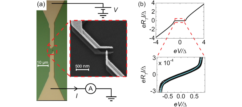
We employ a tunnel junction with a normal metal–insulator–superconductor (NIS) structure, see Fig. 1(a). The essentially constant DOS in the normal metal renders the NIS junction an ideal probe for the superconductor DOS. Due to the BCS energy gap in an NIS system, the tunneling current is expected to be exponentially suppressed with decreasing temperature. Yet in the experiments a small sub-gap current persists as shown in Fig. 1(b). This leakage is typically attributed to Andreev current eiles1993 ; pothier1994 ; hergenrother1994 ; rajauria2008 , smeared DOS of the superconductor nahum1993 , non-vanishing DOS in the insulator within the gap jung2009 , non-equilibrium quasiparticles martinis2009 , or physical imperfections in the junction. Our junctions, like the one in Fig. 1, are made opaque with large normal-state resistance to efficiently suppress the Andreev current. A convenient way to account for the smearing of the characteristics is to use the so-called Dynes model dynes1978 ; dynes1984 based on an expression of the BCS DOS with life-time broadening. The Dynes DOS, normalized by the corresponding normal-state DOS, is given by
| (1) |
where is the BCS energy gap. A non-vanishing introduces effectively states within the gap region, , as opposed to the ideal BCS DOS obtained with resulting in vanishing DOS within the gap. This model reproduces the features observed in our measurements as is shown in Fig. 1(b). We show that, effectively, the Dynes DOS can be produced from the ideal BCS DOS by weak dissipative environment at temperature promoting photon assisted tunneling. A similar environment model with comparable parameter values has also been introduced by other authors to explain, e.g., observations of excess errors in normal-state electron pumps keller1998 ; martinis1993 and Andreev reflection dominated charge transport at low bias voltages in NISIN structures hergenrother1995 .
Theoretical results—For inelastic one-electron tunneling, the rates in forward () and backward () directions through an NIS junction can be written as
| (2) | |||||
at bias voltage . Here, refers to the probability density for the electron to emit energy to the environment ingold1992 . The occupations in the normal and superconducting leads are given by the Fermi functions , respectively. In an ideally voltage-biased junction, . The current through the junction at low temperature of the leads, , is then . Thus we obtain the well-known expression for the conductance of the junction as
| (3) |
In view of Eq. (1), the non-zero linear conductance at low bias voltages, typically observed in experiments as shown in Fig. 1(b), suggests that the superconductor has non-vanishing constant density of states within the gap. Within the Dynes model of Eq. (1), the normalized DOS at low energies, , equals , the ratio of the conductance at zero bias and that at large bias voltages. Although this approach is correct mathematically, it is hard to justify the presence of subgap states physically.

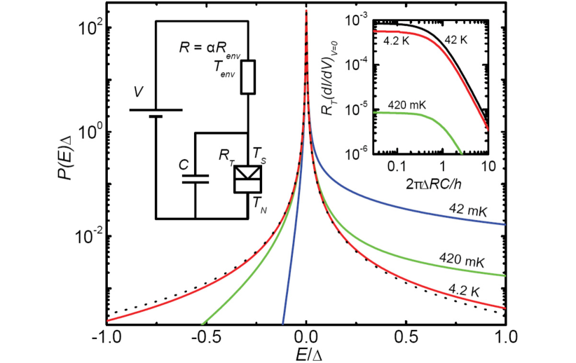
Here, we base our analysis on the pure BCS DOS () and show that the Dynes model in Eq. (1) is consistent with weakly dissipative environment when Eq. (2) is used to obtain the current . The effective resistance value of the environment arises generally from a possibly larger real part of the environment impedance, , which is suppressed by a factor of due to low-temperature filtering, see Fig. 2. With this environment, one obtains the probability density in the limit of small and for energies as a Lorentzian online
| (4) |
where . As the current of an NIS junction is determined by the values of at , we can apply Eq. (4) when , see Fig. 2 for a numerical demonstration. For a general symmetric and , one obtains from Eq. (2) in analogy with Eq. (3): , and
| (5) |
where the effective DOS is given by the convolution
| (6) |
For the weak resistive environment described by Eq. (4), the convolution of a Lorentzian gives
| (7) |
This expression is identical to the Dynes DOS in Eq. (1) by setting , with the equivalent inverse lifetime . The correspondence between the theory and the Dynes model, our main theoretical result, is valid for non-zero lead temperatures as well, as we show in the supplementary material online . Below, we present numerical and experimental studies verifying our claim.

Experiments on single junctions—The leakage induced by the electromagnetic environment can be decreased by efficient rf filtering of the leads and electromagnetic shielding of the sample. One way to do this without affecting the properties of the junction itself is to increase the capacitance across it, see Fig. 2. In this way one approaches the case of an ideally voltage biased junction. In Fig. 2, we present the zero-bias conductance of an NIS junction as a function of the shunting capacitance, , based on the full numerical calculation. For low , the result using Eq. (7) is valid, but for sufficiently high , i.e., for , the leakage decreases significantly demonstrating that capacitive shunting is helpful in suppressing the photon assisted tunneling.
To probe the effect of the capacitive shunting in our experiments, we introduced a ground plane under the junctions. The junctions were made on top of an oxidized silicon wafer, where first a conductive thick layer working as the ground plane was sputtered. On top of this, a thick insulating high-quality film was formed by atomic layer deposition. The junctions were patterned by conventional soft-mask electron beam lithography on top of . For comparison, junctions were made both with and without the ground plane.
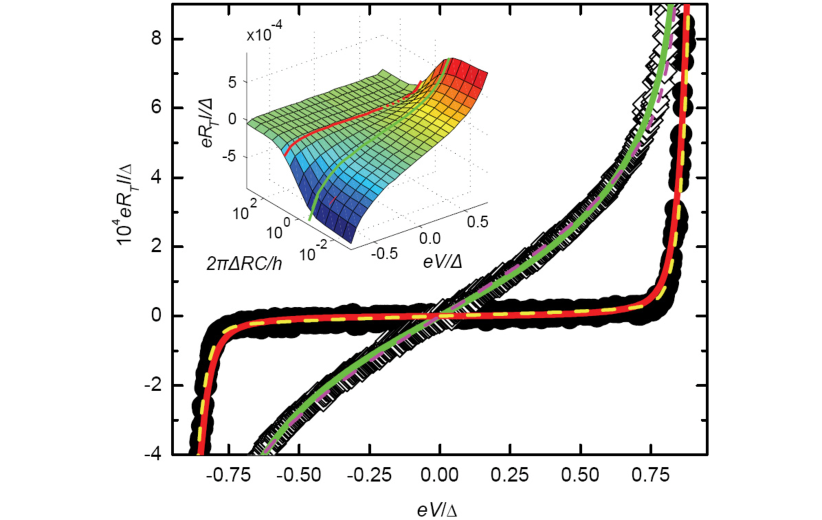
The experiments reported here were performed in a 3He-4He dilution refrigerator with a base temperature of about 50 mK. All the leads were filtered using 1.5 m of Thermocoax cable between the 1 K stage and the sample stage at the base temperature. The curves such as the one in Fig. 1(b) are thermally smeared at elevated temperatures, but below 200 mK we observe hardly any temperature dependence. Figure 3 shows the curves measured at the base temperature for one junction on top of a ground plane and for a similar junction without the ground plane, together with numerical results from the theory. The capacitive shunting decreases the zero-bias conductance significantly. The shunt capacitance values employed in the theory, and , respectively, match well with the estimates for the experimental values in each case. The sample without a ground plane with pF is already entering the regime, where the capacitance is too small to play a role. We used an effective environment resistance of at K, close to the values inferred by Hergenrother et al. hergenrother1995 in the case of incomplete shielding. However, the choice of is somewhat arbitrary here: K with correspondingly lower would yield a slightly improved fit to the data, but K, the temperature of the outer shield, was chosen as a natural surrounding in the measurement set-up. Our results with capacitive shunting, on the other hand, correspond to much improved shielding in the language of Ref. hergenrother1995 . Although the experiments of Ref. hergenrother1995 are quite different from ours, their situation resembles ours in the sense that photons with a very high frequency of GHz are responsible for tunneling.
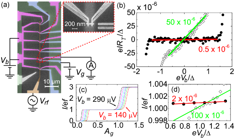
SINIS turnstile—As a practical application, we discuss the SINIS turnstile which is a hybrid single-electron transistor (SET) and a strong candidate for realizing the unit ampere in quantum metrology pekola2008 ; kemppinen2009 ; lotkhov2009 ; kemppinen2009b ; maisi2009 . In the previous experimental studies pekola2008 ; kemppinen2009 ; kemppinen2009b , its accuracy was limited by the sub-gap leakage. Here we test the influence of the ground plane on the flatness of the current plateaus at multiples of , where is the operating frequency. The ground plane had a 20 m wide gap under the SET to reduce the stray capacitance to the rf gate. The ground plane layer was covered by a 300 nm thick insulating layer of spin-on glass, on top of which the rf gate and dc leads were evaporated. Another 300 nm spin-on glass layer was used to cover the rf gate, and the SET was fabricated on top of this layer. The device is shown in Fig. 4(a). This sample geometry is designed for parallel pumping maisi2009 , but here we concentrate on a single device.
Figure 4(b) shows that in this case, the introduction of the ground plane reduces the sub-gap leakage by roughly two orders of magnitude as opposed to a typical turnstile without the ground plane (the latter data from Ref. kemppinen2009b ). In the turnstile operation, the current was recorded as a function of the amplitude of the sinusoidal rf drive, , at several bias voltages. In Fig. 4(c), we show the quantized current plateau at MHz, and the averaged current on this plateau is given in Fig. 4(d) as a function of the bias voltage. The differential conductance at the plateau divided by the asymptotic conductance of the SET is . This result is much improved over those of the earlier measurements pekola2008 ; kemppinen2009 ; lotkhov2009 , and that of the reference sample without the ground plane.

In conclusion, we have shown analytically that the Dynes density of states can originate from the influence of the electromagnetic environment of a tunnel junction, and it is not necessarily a property of the superconductor itself. Our experiments support this interpretation: we were able to reduce the leakage of an NIS junction by an order of magnitude by local capacitive filtering. We stress that capacitive shunting does not necessarily suppress the subgap leakage of an NIS junction, if the leakage is caused by the poor quality of the junction, or by true states within the gap due to, e.g., the inverse proximity effect giazotto2006 . Protecting the junctions against photon assisted tunneling improves the performance of, e.g., single-electron pumps. Contrary to the resistive environment aiming at the same purpose lotkhov2009 , capacitive shunting does not limit the tunneling rates.
We thank D. Averin, P. Delsing, M. Gustafsson, S. Lotkhov, A. Manninen, M. Paalanen, and V. Shumeiko for discussions and M. Meschke, J. Peltonen, and I. Iisakka for technical support. This work has been supported by Technology Industries of Finland Centennial Foundation, the Academy of Finland, Emil Aaltonen Foundation, CREST-JST, MEXT kakenhi ”Quantum Cybernetics”, and the European Community s Seventh Framework Programme under Grant Agreements No. 217257 (EURAMET joint research project REUNIAM) and No. 218783 (SCOPE).
References
- (1) Ya. M. Blanter and M. Büttiker, Phys. Rep. 336, 1 (2000).
- (2) Quantum Computing with Superconducting Qubits, Quantum Inf. Process. 8, pp. 51-281 (2009).
- (3) F. Giazotto et al., Rev. Mod. Phys. 78, 217 (2006).
- (4) J. P. Pekola et al., Nature Phys. 4, 120 (2008).
- (5) J. Bardeen, L. N. Cooper, and J. R. Schrieffer, Phys. Rev. 108, 1175 (1957).
- (6) G. C. O’Neill et al., J. Low Temp. Phys. 151, 70 (2008).
- (7) S. Rajauria et al., J. Low Temp. Phys. 153, 325 (2008).
- (8) P. Koppinen et al., J. Low Temp. Phys. 154, 179 (2009).
- (9) H. Jung et al., Phys. Rev. B 80, 125413 (2009).
- (10) D. C. Ralph et al., Phys. Rev. Lett. 74, 3241 (1995).
- (11) R. C. Dynes et al., Phys. Rev. Lett. 41, 1509 (1978).
- (12) R. C. Dynes et al., Phys. Rev. Lett. 53, 2437 (1984).
- (13) G. L. Ingold and Yu. V. Nazarov, in Single charge tunneling, Vol. 294 of NATO ASI Series B, edited by H. Grabert and M. H. Devoret (Plenum Press, New York, 1992), pp. 21–107.
- (14) D. V. Averin and Yu. V. Nazarov, Phys. Rev. Lett. 65, 2446 (1990).
- (15) A. F. Andreev, Zh. Eksp. Teor. Fiz. 46, 1823 (1964); Sov. Phys. JETP 19, 1228 (1964).
- (16) G. E. Blonder et al., Phys. Rev. B 25, 4515 (1982).
- (17) T. M. Eiles et al., Phys. Rev. Lett. 70, 1862 (1993).
- (18) H. Pothier et al., Phys. Rev. Lett. 73, 2488 (1994).
- (19) J. M. Hergenrother et al., Phys. Rev. Lett. 72, 1742 (1994).
- (20) S. Rajauria et al., Phys. Rev. Lett. 100, 207002 (2008).
- (21) M. Nahum and J. M. Martinis, Appl. Phys. Lett. 63, 3075 (1993).
- (22) J. M. Martinis et al., Phys. Rev. Lett. 103, 097002 (2009).
- (23) M. W. Keller et al., Phys. Rev. Lett. 80, 4530 (1998).
- (24) J. M. Martinis and M. Nahum, Phys. Rev. B 48, 18316 (1993).
- (25) J. M. Hergenrother et al., Phys. Rev. B 51, 9407 (1995).
- (26) See EPAPS supplementary material for derivation.
- (27) A. Kemppinen et al., Eur. Phys. J. Spec. Top. 172, 311 (2009).
- (28) S. V. Lotkhov et al., Appl. Phys. Lett. 95, 112507 (2009).
- (29) A. Kemppinen et al., Appl. Phys. Lett. 94, 172108 (2009).
- (30) V. F. Maisi et al., New J. Phys. 11, 113057 (2009).