Tuning mechanical modes and influence of charge screening in nanowire resonators
Abstract
We probe electro-mechanical properties of InAs nanowire (diameter 100 nm) resonators where the suspended nanowire (NW) is also the active channel of a field effect transistor (FET). We observe and explain the non-monotonic dispersion of the resonant frequency with DC gate voltage (). The effect of electronic screening on the properties of the resonator can be seen in the amplitude. We observe the mixing of mechanical modes with . We also experimentally probe and quantitatively explain the hysteretic non-linear properties, as a function of , of the resonator using the Duffing equation.
pacs:
Nano electro mechanical systems (NEMS) Ekinci and Roukes (2005), are being used extensively to study small displacements Knobel and Cleland (2003), mass sensing Yang et al. (2006); Jensen et al. (2008); Lassagne et al. (2008); Chiu et al. (2008), spin-torque effect Zolfagharkhani et al. (2008), charge sensing Rugar et al. (2004), Casimir force Munday et al. (2009) and potential quantum mechanical devices LaHaye et al. (2004); Regal et al. (2008). A variety of NEMS devices, fabricated using carbon nanotubes Sazonova et al. (2004); Steele et al. (2009); Lassagne et al. (2009); Huttel et al. (2009a, b), graphene Bunch et al. (2007); Chen et al. (2009); Garcia-Sanchez et al. (2008), nanowires (NWs) of silicon Feng et al. (2007) and by micromachining bulk silicon Carr et al. (1999), have been used to probe the underlying physics at nano scale. In this work we study the electromechanical properties of doubly clamped suspended n-type InAs NWs. In our suspended NW FET, the gate electrode serves three purposes: first, to modify the tension in the NW, second, to actuate the mechanical motion of the resonator and third, enabling us to systematically study the coupling of mechanical properties to the tunable electron density. As we will show, a tunable electron density leads to a variable screening length of the order of the nanowire’s cross sectional dimensions. Thus the electro-mechanical properties enter into a mesoscale regime. Such a variable electron density is not accessible in carbon nanotubes; the screening length cannot be tuned continuously – relative to the diameter of the carbon nanotube – as easily. However, the physics of charge screening in nanoscale capacitors Black and Welser (1999) and ferroelectric devices Stengel and Spaldin (2006) is intimately connected to that in our NEMS devices. Taken together, these observations suggest that a geometrical interpretation of capacitance is inadequate at the nano scale. Additionally, the gate allows us to tune the resonant frequency non-monotonically due to the competition between the electrostatic force and the mechanical stiffness ( N/m) of the nanowire, a feature expected (but heretofore not studied in detail) for all electrostatically actuated NEMS. In this article, we demonstrate that the InAs semiconducting nanowire system manifests this transition from softening to hardening as the gate voltage is varied. In addition, mixing of the natural mechanical modes as a function of can be understood in terms of the structural asymmetries in the resonator. In the non-linear regime we study in detail hysteretic behavior as a function of (unlike the commonly studied response as a function of drive frequency) and we show that this can be understood by using the Duffing equation incorporating the effect of gate voltage. The observed hysteretic response with is an alternate knob for tuning the nonlinear response of our NEMS devices and can be used for charge detection Kr mmer and et al. (2000). Our work provides further understanding of the unique characteristics of NEMS devices operating at room temperature. The observed behavior can provide information on the nanomechanics of other systems whose electron density, stiffness or screening length cannot be so readily tuned.
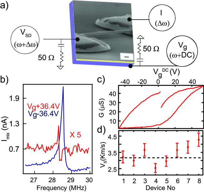
The InAs NWs used for this work were grown using metal organic vapor phase epitaxy (MOVPE) Duan and Lieber (2000); Dhara et al. (2009). The NWs are oriented in the direction and are 80 to 120 nm in diameter with a length of several micrometers. The substrate used for making the devices is a degenerately doped silicon wafer with 300 nm thick SiO2. We have fabricated suspended InAs NW devices by sandwiching the NWs between two layers of electron-beam resist and then using electron beam lithography to define the electrodes and suspend them by depositing 150 nm Cr and 250 nm Au after development followed by in situ plasma cleaning Dhara et al. (2009). The ohmic contacts also serve as mechanical supports for the NW suspended 200 nm above the surface of SiO2. Fig.1a shows the SEM image of a resonator device and scheme for actuating and detecting the motion of the resonator. All the measurements were done at 300 K and pressure less than 1 mBar.
To actuate and detect the resonance we use the device as a heterodyne mixer Chiu et al. (2008); Sazonova et al. (2004); Sazonova (2006); Knobel et al. (2002); He et al. (2008); Chen et al. (2009). We use electrostatic interaction between the wire and gate to actuate the motion in a plane perpendicular to the substrate. We apply a radio frequency (RF) signal and a DC voltage at the gate terminal using bias-tee. Another RF signal is applied to the source electrode (Fig.1a). The RF signal applied at the gate modulates the gap between NW and substrate at angular frequency , and alters the overall tension in the NW. The amplitude of the current through the NW at the difference frequency (), also called the mixing current , can be written as Sazonova et al. (2004)
| (1) | |||||
where is the conductance of the NW, is the charge induced by the gate, is the gate capacitance, is the amplitude of oscillation at the driving frequency and z axis is perpendicular to the substrate. The term is the background mixing current which is independent of the oscillation of the NW and depends on the amplitude of oscillation. Measuring using a lock-in allows us to monitor the resonance of the NW as the frequency is swept. Fig.1b shows as a function of for = 36.4 V. The sharp feature corresponds to the mechanical resonance of the NW. We address the asymmetry of the mixing current signal for later. Fig.1c shows the plot of conductance () as a function of . The variation of with is very critical for this scheme of heterodyne mixing to work as it controls the overall amplitude . The hysteresis observed in the measurement of conductance is typical for our suspended devices and is associated with charge trap states with dipolar nature on surface of the nanowire Dayeh et al. (2007); Li et al. (2007).
We can connect the resonant frequency of the fundamental mode, , of a doubly clamped beam at zero , to the material properties of the beam as where is the velocity of sound; is the radius of the beam, is the length of the beam, is the Young’s modulus, is the density of the material and . Fig.1d shows a plot for that does not vary much from the bulk value Levinshtein (1996) (dashed line) for eight different devices. The scatter around the calculated using bulk values could be due to the relative volume fraction contribution of the amorphous layer around the NWs; this needs further detailed study.
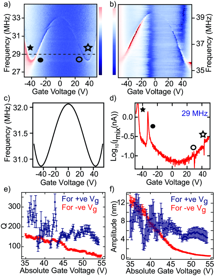
Fig.2a and 2b show the colorscale plot of as a function of and on a logscale spanning more than 3 decades. Data is taken by sweeping for each value of frequency. In the data from both the devices we see a symmetric evolution of the resonant frequency as a function of . The parabolic behavior is expected as the attractive force exerted by the gate on the wire is given by . An increase in enhances the tension in the NWSapmaz et al. (2003). We now discuss the particular W-shaped dispersion of modes as a function of . As is increased, initially the mode disperses negatively and after a certain threshold voltage it disperses with a positive slope. Although purely negatively and positively dispersing modes have been studied in detail before by Kozinsky et al. Kozinsky et al. (2006), we observe the crossover regime where these interactions compete. This particular dispersion can be understood using a toy-model in which a wire is suspended from a spring of force constant Ki above the substrate. The wire and the substrate make up the two electrodes of a capacitor. There are two consequences of increasing : first, it changes the equilibrium position by moving the NW closer to the substrate and second, it makes the local potential asymmetric and less steep. The effective force constant, Keff, is reduced, resulting in negative dispersion of the mode for . If the intrinsic force constant Ki had been independent of , the modes would always disperse negatively when motion occurs perpendicular to the gate plane. However, in general Ki can be written as ); where , , and are constants. With then, to a first approximation, Keff K. We find that the W-shape of the dispersion curve can be explained only if one considers the case where . The result of such calculations (Fig.2c) quantitatively explains the experimental observations. , the value at which the crossover from negative to positive dispersion occurs is a function of the dimensions of the NW and the capacitive geometry of the device. The effect of the device dimension is clearly seen in a larger value of in device-2 shown in Fig.2b where the doubly clamped beam is 120 nm thick, as against 100 nm for device-1 in Fig.2a (the lengths differ by 200 nm).
Next, we consider another complementary aspect of the data – the amplitude of the mixing current. Fig.2d shows (log-scale) as a function of . We see that the amplitude of the mixing current for the negative values of are significantly larger than those for positive for the same mechanical mode; this is also seen in Fig.1b. We now try to understand this asymmetry as our InAs NW are n-type semiconductors Dhara et al. (2009) as seen in Fig.1c. To understand this asymmetry we have carried out detailed fits of the experimental data for the amplitude of mixing current as a function of frequency using Eqn.1. The amplitude of oscillation at frequency is given by
| (2) |
where is the amplitude at resonant frequency , is the quality factor and is the relative phase difference between the and signals that depends on the device parameters like the contact resistance. Fitting from Eqns.1 and 2 allow us to extract the variation of as a function of as shown in Fig.2e (why ). We have also estimated the amplitude of oscillation using Eqns.1 and 2 by examining the ratio . A plot of the calculated amplitude () is seen in Fig.2f. We see that as the is increased and are observed to decrease. We also observe that there are noticeable differences in and for positive and negative values of . The values of and are larger for positive . One of the possible mechanisms that can explain this behavior in the amplitude is that with increasing one increases the density of electrons in the NW leading to reduction in the screening length. This implies that the simple geometrical capacitance is inaccurate particularly since the screening length can be comparable to NW diameter at low densities (at negative in our case). In our device geometry, using Thomas-Fermi approximation Black and Welser (1999), screening length is around 20-40 nm (diameter of our devices are 100 nm) and the distance between the nanowires and gate oxide 200nm. So, the screening length is a significant fraction of the diameter and the suspension distance - this plays a critical role in observing the effect of density gradients within the cross-section of the nanowire. In case of single walled carbon nanotube, diameter is 1-2 nm and height of suspension is typically 100nm or more Steele et al. (2009); Lassagne et al. (2009); Huttel et al. (2009a, b). Additionally the screening length in carbon nanotubes is typically several multiples of the nanotube diameter Sasaki (2002), so due to an increased ratio of suspension distance to diameter and the large screening length compared to the diameter it is very difficult to observe the physics we discuss for the case of nanowires in carbon nanotubes. We would like to point out that this is not a peculiarity of the InAs nanowires and should be seen in other semiconducting nanowire devices as well with similar dimensions. Additionally, if one considers the realistic case with non-uniform density of carriers in the NW due to the device geometry Khanal and Wu (2007) the NW will have a gradient of dielectric constant Richardson and Vinsome (1971). A gradient of dielectric constant Unterreithmeier et al. (2009) alongwith a change in capacitance as a function of the density changes the capacitive coupling of the NW to the gate. This results in differing amplitudes for two different electron densities. Our device geometry with NW diameter comparable to the gap accentuates this effect.
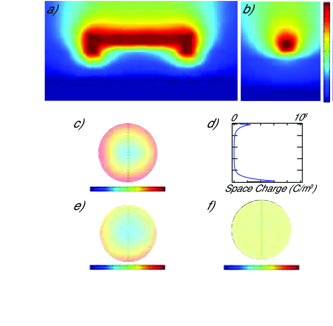
In order to better understand the effect of the gate voltage in tuning the spatial charge density across the cross-section of the nanowire we selfconsistently solve three dimensional Poisson’s equation using finite element method for our device geometry. We use approach followed by Khanal et al. Khanal and Wu (2007) by solving , throughout the space of the nanowire and its dielectric environment (here is dielectric constant, is the local electrostatic potential in the system due to applied gate voltage, and is space charge density inside the NW). The geometry consists of a 100 nm diameter and 1.5 m long InAs nanowire clamped by metallic electrodes. The wire is suspended 100 nm above a 300 nm thick silicon-oxide dielectric on the gate electrode. Inside the nanowire the where is the charge of an electron, is the density of the n-type dopants (cm-3), and are the densities of electrons and holes. The unintentional source of n-type dopants in our growth is Si and C, from the metal organic precursors and are assumed to be uniformly distributed throughout the nanowire. A selfconsistent calculation gives us the distribution of potential throughout the space and space charge density in the nanowire. Fig.3a and 3b show the colourscale distribution of potential when the V. In order to model the consequences of modifying gate voltage we calculated the distribution of space charge density through the nanowire for and V. Fig.3c, 3d, 3e, and 3f show the result of such a calculation for varying for space charge density in the center of the NW. For positive voltages the Fermi energy is very close to the conduction band of the InAs and as a result the charge density is very uniform while behaving as a metal like system. This simple modeling supports our arguments that a gradient of electron density can modify the capacitive coupling and the resulting amplitude. Further analysis is needed to solve self consistent solutions to the Poisson’s equation where the dielectric constant is itself a function of the density and the quantitative variation of and amplitude with sign of . Our measurements suggest a way to tune the efficiency of actuation by tuning the density of carriers.
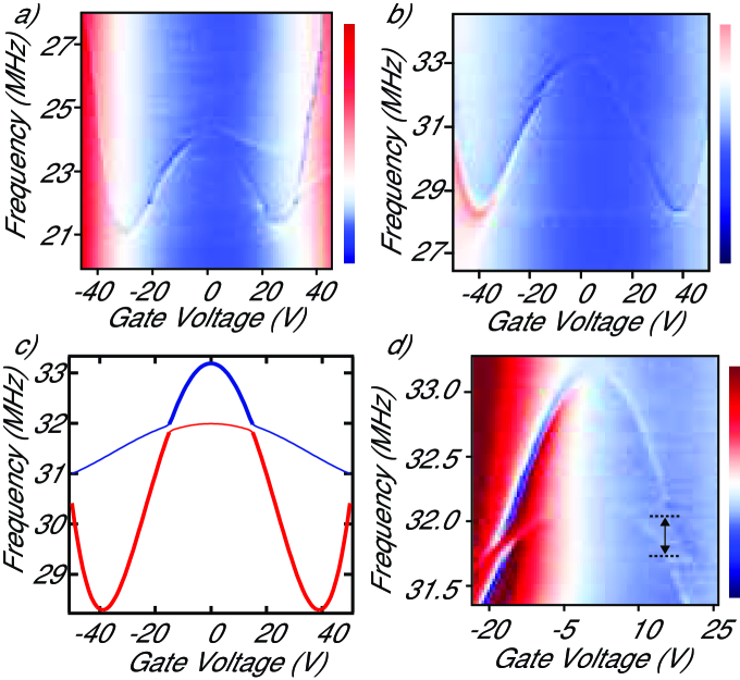
We next consider three other features of our data – first, the presence of other mechanical modes near the fundamental mode; second, the mixing of modes as a function of the , and third, the non-linear properties of NW oscillators driven to large amplitudes. Fig.4a and 4b show the plot of as a function of and for device-3 and device-2. It is well known that for a doubly clamped beam with no tension, with , and for the transverse modes. It is clear that if the fundamental mode () is described by a mode with zero nodes and moving in a plane perpendicular to the substrate, the other observed modes, in the frequency range near (Fig.4a, 4b), cannot be defined by and . We have observed the anticipated and modes at higher frequencies. The other modes beside the fundamental in Fig.4a, 4b, are explained due to geometrical asymmetry along the diameter in the NW (Fig.4c, details of this calculation provided in Supporting Information). These are the modes involving motion in a plane that is not perpendicular to the substrate. This would explain the less steep slope of the dispersion as a function of .
Fig.4a and 4b also show the mixing of the modes as a function of . The mode mixing can be seen clearly in Fig.4d which shows a close-up of the data in Fig.4b. Displacement along the transverse direction (perpendicular to ) will weakly affect the capacitance because of any slight asymmetry in the physical structure of the NW. The coupling coefficient appearing in the potential energy gives rise to mode-mixing (see Supporting Information). For the device shown in Fig.4b the minimum frequency gap in the region of level repulsion is MHz. The asymmetry in the amplitude of the modes away from the region of mixing can also be understood within this model.
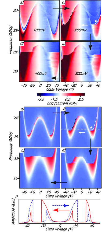
We next consider the non-linear response of these NEMS oscillators. Due to electrostatic actuation, the potential energy of the oscillator is asymmetric about the equilibrium position and has the form , where , and are coefficients depending on . We have experimentally probed the non-linear and hysteretic response of the device. Fig.5a, 5b, 5c, and 5d, show the experimentally measured non-linear response of this device leading to hysteretic behavior as function of with increasing amplitude of driving force. Here, is swept at a given drive frequency to measure the mixing current and several such sweeps are collated (the distinct response of sweeping the frequency at a fixed – a common mode to study non-linear response – is described in supporting information). There are two features that we would like to point out – first, in the region at the bottom of the W-shaped dispersion curve, two branches of the same mode merge into one broad peak where the oscillator has large amplitude over a wide range of and second, whenever during the sweep, one crosses the region with a local negative value for (here, is the resonant frequency at a particular ), shows a curved hysteretic j-shaped response (indicated by ), seen in Fig.5b. In order to understand and explain the experimentally observed hysteretic response as a function of , we have used the Duffing equation Landau and Lifshitz (1976) for our resonator. The result of such a calculation for amplitude is seen in Fig.5e, 5f, 5g, and 5h, with increasing amplitude of driving force. To calculate the amplitude we have only used the observed dispersion relation (W shape) as input for Duffing equation. There is a qualitative agreement between the experimentally measured data shown in Fig.5a-d and results of calculation using the Duffing equation shown in Fig.5e-h. We find that for every increase in excitation amplitude by 100 mV corresponds to an increase of a factor of 2.5 in the anharmonic component of the Duffing equation (from observing the calculated data). Additional aspect of the nonlinearity of the oscillator is also seen in the evolution of dispersion near as the actuation amplitude is gradually increased from 100 mV to 400 mV in Fig.5a-d. The negative dispersion is due to the softening of electrostatic force and with larger amplitude of oscillation the effective spring constant changes, as the wire samples a region with varying electric field; this difference is clearly seen in the dispersion near for the data shown in Fig.5 a and d.
Fig.5i, shows the line plot (along the dashed line in Fig.5f) of calculated amplitude for different sweep direction of and the resulting hysteresis. The observed hysteretic response, as a function of , is quite different from the hysteretic response as a function of drive frequency ( discussed in supporting information ). This non-linear response of our devices with may be utilized for charge detection Kr mmer and et al. (2000) as near the onset of non-linearity the change in amplitude as a function of is very large.
In summary, we have studied the electromechanical properties of doubly clamped InAs NW resonators. Their size and tunable electron density allow us to map behavior that has not been manifested in a single device. We have observed and quantitatively explained the competition between the softening of stiffness of the restoring force of the resonator due to the variation of the electrostatic force under variable gate voltage. At larger voltages, the stretching of the nanowire leads to increased stiffness resulting in a non-monotonic dispersion of the fundamental mode with . The screening of electric fields due to the variation in the density of the electrons in our suspended FET devices modifies the amplitude because the variation of the screening length spans the cross sectional dimension of our nanowire. Further, the non-linear properties of our device can be understood qualitatively using the Duffing equation that explains the hysteretic response of the amplitude as a function of gate voltage. Thus in a single device, we demonstrate, separate and account for three diverse behaviors. Our measurements indicate that measuring electromechanical response influenced by charge screening could lead, in the future, to new ways to probe spin physics by exploiting spin-dependent charge screening Zhang (1999). Probing the physics by tuning electron density in NEMS devices may help probe the role of defects Poklonski and Stelmakh (1983) and electron hopping as one moves from insulating to conducting regimes. Control over the non-linear dynamics may be achievable by controlling mode mixing and DC gate voltage.
This work was supported by Government of India. J. Parpia was supported by DMR-0457533.
References
- Ekinci and Roukes (2005) K. L. Ekinci and M. L. Roukes, Review of Scientific Instruments 76, 061101 (2005).
- Knobel and Cleland (2003) R. G. Knobel and A. N. Cleland, Nature 424, 291 (2003).
- Yang et al. (2006) Y. T. Yang, C. Callegari, X. L. Feng, K. L. Ekinci, and M. L. Roukes, Nano Letters 6, 583 (2006).
- Jensen et al. (2008) K. Jensen, K. Kim, and A. Zettl, Nat Nano 3, 533 (2008).
- Lassagne et al. (2008) B. Lassagne, D. Garcia-Sanchez, A. Aguasca, and A. Bachtold, Nano Letters 8, 3735 (2008).
- Chiu et al. (2008) H.-Y. Chiu, P. Hung, H. W. C. Postma, and M. Bockrath, Nano Letters 8, 4342 (2008).
- Zolfagharkhani et al. (2008) G. Zolfagharkhani, A. Gaidarzhy, P. Degiovanni, S. Kettemann, P. Fulde, and P. Mohanty, Nat Nano 3, 720 (2008).
- Rugar et al. (2004) D. Rugar, R. Budakian, H. J. Mamin, and B. W. Chui, Nature 430, 329 (2004).
- Munday et al. (2009) J. N. Munday, F. Capasso, and V. A. Parsegian, Nature 457, 170 (2009).
- LaHaye et al. (2004) M. D. LaHaye, O. Buu, B. Camarota, and K. C. Schwab, Science 304, 74 (2004).
- Regal et al. (2008) C. A. Regal, J. D. Teufel, and K. W. Lehnert, Nat Phys 4, 555 (2008).
- Sazonova et al. (2004) V. Sazonova, Y. Yaish, H. Ustunel, D. Roundy, T. A. Arias, and P. L. McEuen, Nature 431, 284 (2004).
- Steele et al. (2009) G. A. Steele, A. K. Huttel, B. Witkamp, M. Poot, H. B. Meerwaldt, L. P. Kouwenhoven, and H. S. J. van der Zant, Science 325, 1103 (2009).
- Lassagne et al. (2009) B. Lassagne, Y. Tarakanov, J. Kinaret, D. Garcia-Sanchez, and A. Bachtold, Science 325, 1107 (2009).
- Huttel et al. (2009a) A. K. Huttel, G. A. Steele, B. Witkamp, M. Poot, L. P. Kouwenhoven, and H. S. J. van der Zant, Nano Letters 9, 2547 (2009a).
- Huttel et al. (2009b) A. K. Huttel, B. Witkamp, M. Leijnse, M. R. Wegewijs, and H. S. J. van der Zant, Physical Review Letters 102, 225501 (2009b).
- Bunch et al. (2007) J. S. Bunch, A. M. van der Zande, S. S. Verbridge, I. W. Frank, D. M. Tanenbaum, J. M. Parpia, H. G. Craighead, and P. L. McEuen, Science 315, 490 (2007).
- Chen et al. (2009) C. Chen, S. Rosenblatt, K. I. Bolotin, W. Kalb, P. Kim, I. Kymissis, H. L. Stormer, T. F. Heinz, and J. Hone, Nat Nano 4, 861 (2009).
- Garcia-Sanchez et al. (2008) D. Garcia-Sanchez, A. M. van der Zande, A. S. Paulo, B. Lassagne, P. L. McEuen, and A. Bachtold, Nano Letters 8, 1399 (2008).
- Feng et al. (2007) X. L. Feng, R. He, P. Yang, and M. L. Roukes, Nano Letters 7, 1953 (2007).
- Carr et al. (1999) D. W. Carr, S. Evoy, L. Sekaric, H. G. Craighead, and J. M. Parpia, Applied Physics Letters 75, 920 (1999).
- Black and Welser (1999) C. T. Black and J. J. Welser, Electron Devices, IEEE Transactions on 46, 776 (1999).
- Stengel and Spaldin (2006) M. Stengel and N. A. Spaldin, Nature 443, 679 (2006).
- Kr mmer and et al. (2000) H. Kr mmer and et al., EPL (Europhysics Letters) 50, 101 (2000), 0295-5075.
- Duan and Lieber (2000) X. Duan and C. M. Lieber, Advanced Materials 12, 298 (2000).
- Dhara et al. (2009) S. Dhara, H. S. Solanki, V. Singh, A. Narayanan, P. Chaudhari, M. Gokhale, A. Bhattacharya, and M. M. Deshmukh, Physical Review B 79, 121311 (2009).
- Sazonova (2006) V. Sazonova, Ph.D. thesis, Cornell University (2006).
- Knobel et al. (2002) R. Knobel, C. S. Yung, and A. N. Cleland, Applied Physics Letters 81, 532 (2002).
- He et al. (2008) R. He, X. L. Feng, M. L. Roukes, and P. Yang, Nano Letters 8, 1756 (2008).
- Dayeh et al. (2007) S. A. Dayeh, C. Soci, P. K. L. Yu, E. T. Yu, and D. Wang, Applied Physics Letters 90, 162112 (2007).
- Li et al. (2007) H. Y. Li, O. Wunnicke, M. T. Borgstrom, W. G. G. Immink, M. H. M. van Weert, M. A. Verheijen, and E. P. A. M. Bakkers, Nano Letters 7, 1144 (2007).
- Levinshtein (1996) M. Levinshtein, Handbook Series On Semiconductor Parameters, vol. 1 (World Scientific Publishing Company, 1996).
- Sapmaz et al. (2003) S. Sapmaz, Y. M. Blanter, L. Gurevich, and H. S. J. van der Zant, Physical Review B 67, 235414 (2003).
- Kozinsky et al. (2006) I. Kozinsky, H. W. C. Postma, I. Bargatin, and M. L. Roukes, Applied Physics Letters 88, 253101 (2006).
- (35) Our devices show relatively low ( 150-600 ) as gold is soft and clamping losses could result.
- Sasaki (2002) K. Sasaki, Physical Review B 65, 195412 (2002).
- Khanal and Wu (2007) D. R. Khanal and J. Wu, Nano Letters 7, 2778 (2007).
- Richardson and Vinsome (1971) P. K. W. Richardson and D. Vinsome, Journal of Physics C: Solid State Physics 4, 2650 (1971), 0022-3719.
- Unterreithmeier et al. (2009) Q. P. Unterreithmeier, E. M. Weig, and J. P. Kotthaus, Nature 458, 1001 (2009).
- Landau and Lifshitz (1976) L. Landau and E. Lifshitz, Course of theoretical physics: Mechanics, vol. 1 (Butterworth-Heinemann, 1976).
- Zhang (1999) S. Zhang, Physical Review Letters 83, 640 (1999).
- Poklonski and Stelmakh (1983) N. A. Poklonski and V. F. Stelmakh, Physica Status Solidi (B) 117, 93 (1983).