Coulomb screening and collective excitations in biased bilayer graphene
Abstract
We have investigated the Coulomb screening properties and plasmon spectrum in a bilayer graphene under a perpendicular electric bias. The bias voltage applied between the two graphene layers opens a gap in the single particle energy spectrum and modifies the many-body correlations and collective excitations. The energy gap can soften the plasmon modes and lead to a crossover of the plasmons from a Landau damped mode to being undamped. Plasmon modes of long lifetime may be observable in experiments and may have potentials for device applications.
pacs:
71.10.-w,75.10.Lp,75.70.Ak,71.70.GmBilayer graphene (BLG) has attracted much attention due to its unique electronic characteristics, distinct from the Dirac gas in monolayer graphene and the Fermi gas in traditional semiconductor quantum wells mcca ; wang2 ; hwan . In addition, an energy gap between the conduction and valence bands of a BLG can be opened and tuned by introducing an electrostatic potential bias between the two graphene layers oost ; zhan ; stau ; min ; gava ; falk ; mcca1 ; mcca2 . This can be easily realized via one or more external gates to perpendicularly bias BLG and make it a potential component for integrated electronics. It is then very intriguing to understand some fundamental properties such as correlation and screening properties of electron gases in a biased BLG. As collective excitations, plasmon modes are a direct result of electronic correlation due to Coulomb interaction between electrons. Experimental detection of plasmon modes has recently become feasible and has been used to determine the dynamical behavior of electrons in graphene layers liu ; kram ; bost1 .
Previously, assuming zero or non-zero spin-orbit interaction induced energy gap, we have studied the Coulomb screening and collective excitation spectrum of intrinsic and doped monolayer graphenes at zero and finite temperatures in the random phase approximation (RPA) wang . Later, Qaiumzadeh and Asgari qaiu assumed an unspecified energy gap of arbitrary width for doped monolayer graphene and studied the corresponding ground-state properties at zero temperature in RPA. They concluded that the conductance and charge compressibility decrease with the band gap. Furthermore, a THz source has been proposed based on the stimulated plasmon emission in graphene rana and the absorption of THz electromagnetic radiation in gapped graphene has been estimated wrig . On the other hand, the Coulomb screening and the collective excitations in zero gap BLG have been studied in our previous work at zero and finite temperatures wang2 and by Hwang and Das Sarma hwan for the zero temperature case. In this paper we report on our studies of the correlations, screening, and the plamson spectrum of electron gases in a biased BLG.
In the effective-mass approximation mcca , the Hamiltonian describing electrons of moderate energies in the valley of a biased BLG reads
| (1) |
with and being measured from the point. The effective mass of the quadratic term is with the free electron mass, Å the C-C bond length on the graphene layer, eV the intra-layer coupling, and eV the direct inter-layer coupling. The second term arises from the electrostatic potential bias between the two graphene layers separated by a distance Å. The Hamiltonian is obtained by keeping only the linear term of the Tayler expansion on the small energy value in unit of , so it is valid for electrons of energy less than 0.4 eV which is adequate in our case. The indirect inter-layer coupling is neglected since it affects only the energy band in the range of less than 2 meV from the middle of the conduction-valence band gap wang2 .
The eigenenergy of the above Hamiltonian is with the eigenfunctions and for and respectively. Here is the azimuth of the vector , i.e., , and indicates the ratio of the kinetic energy to the potential bias with . The conduction band which touches the valence band at in unbiased BLG becomes separated from it by an energy gap equal to the potential bias . This gap converts the BLG from a semimetal into a semiconductor and accordingly modifies the optical and electric properties of the electrons inside. For finite , the density of states of the BLG diverges on the edge of the energy gap . At zero temperature, the carrier density in a BLG of Fermi energy is .
Following the well-established formalism for spin systems wang1 , we obtain the dielectric matrix of a biased BLG in the form of a unit matrix multiplied by a dielectric function with the bare Coulomb interaction and the electron-hole propagator
| (2) |
The factor four comes from the degenerate two spins and two valleys at and , is the Fermi function, and the vertex factor reads At or , . Similar to unbiased BLG, the interband vertical and back scatterings are both forbidden but the intraband back scattering is allowed in biased BLG.
It has been shown that the interlayer indirect C-C interaction introduces anisotropic fine structures near the Fermi energy in the range of 2 meV and leads to some interesting dielectric and collective phenomena wang2 . For systems with energy gap meV or with Fermi energy satisfying meV, this anisotropy becomes negligible. For large comparable to , the effect of the ”Maxican hat” at the bottom (top) of the conduction (valence) band mcca should be taken into account. Nevertheless, for moderate and , the model described here should be valid. Furthermore, we assume that the BLG is far enough from the substrate and the gate so a unit background dielectric constant is used in the calculation.
In intrinsic BLG where no net carrier exists, i.e., and the Fermi energy , intraband scattering is only allowed at non-zero temperatures. In Fig. 1, we have shown that the real part (, solid curve) and imaginary part (, dotted) of the dielectric function versus the energy in an intrinsic system with potential bias meV at a finite temperature 77 K for (a) m-1 and (b) m-1. In the small case, the intraband scattering introduces a dip for and a peak for of low energy as illustrated in the insets. Consequently, there exist two plasmon modes, one Landau damped and one almost undamped. The depth and the width of this real part dip increase with the temperature indicating the increase of intraband scattering strength and also the energy of the undamped plasmon mode. At , the threshold of interband single-particle excitation continuum (SPEC), steps up and a sharp peak of is observed thanks to the flat bottom and top of the energy bands. This peak may introduce additional plasmon modes and is similar to the case in gapped monolayer graphene wang . As increases, the dip ( peak) due to intraband scattering shifts quickly to the higher energy side while the peak ( step) due to the interband scattering moves only slowly. As a result, the well separated intra- and inter-band structures at small mix with each other and then separate again when increase as shown in Fig. 1(b).


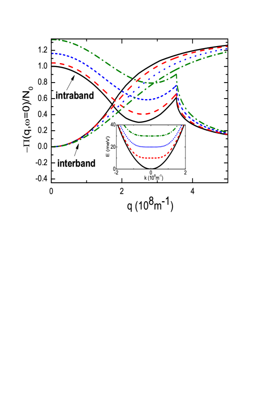
The effect of a bias on the zero-temperature propagator in doped BLG hwan with a fixed carrier density m-2 is studied in Fig. 2. The interband contribution decreases with the bias potential as the energy gap widens. The intraband contribution, on the contrary, increases with the bias since the energy dispersion leads to an enhancement of the density of states near the Fermi energy. Here one of the characteristics in BLG against in monolayer graphene wang2 ; hwan is the strong back scattering of electrons on the Fermi surface which results in an intraband peak at m-1. If the Fermi energy remains fixed as the bias increase, the carrier density decreases and the intra- (inter-) band contribution at large (small) becomes less sensitive to the bias and decreases (increases) with the bias.

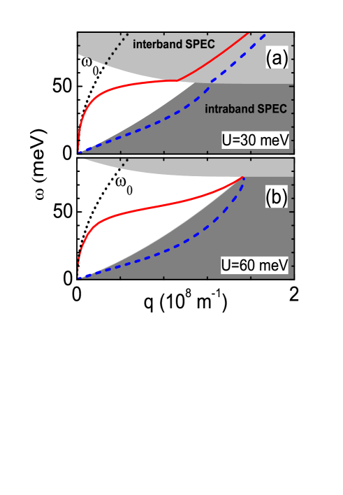
The plasmon modes are obtained by solving the zeros of the real part of the dielectric function and the corresponding imaginary part represents the damping rate of the plasmon modes. In Fig. 3, we plot the typical spectrum of plasmon modes (solid and dashed curves) in doped BLG at zero temperature under potential bias (a) meV and (b) meV. The upper light shadow is the interband SPEC edged at and the lower dark shadow is the intraband SPEC edged at . One undamped mode is located in the SPEC gap due to finite Fermi energy. In the long wavelength limit, its dispersion is the same as that of Fermi 2D gas of two valley, . However, compared to the plasmon dispersion in BLG without bias which is just slightly modified from that of Fermi 2D gas, this dispersion is greatly softened for finite as also shown in Fig. 4. Our numerical analysis shows that this is a result of the deformation near the bottom and top of the energy bands. Note that the lowered plasmon group velocity may be helpful for making a stimulated plasmon oscillator rana . A Landau damped mode is located just below the intraband SPEC edge as usually happens in traditional 2D Fermi gas but is pushed to lower energy at larger . The undamped mode can enter into the interband SPEC and becomes a slightly damped mode in some cases as shown in Fig. 3(a) under meV or merges with the damped mode and disappears near the cross of intra- and inter-band SPEC edges as shown in Fig. 3(b) under meV.

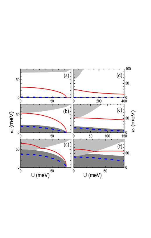
With the plasmon spectrum in mind, we now explore how affects the energy and damping properties of the modes. In the left panels of Fig. 4, we show versus at several typical when keeping the Fermi energy constant. As in Fig. 3, the light shadow indicates the interband SPEC and the dark shadow for the intraband one. At small as illustrated in (a), there is one undamped plasmon mode with energy located inside the SPEC gap of which the width is about and one damped mode of low frequency. When reaches and passes , the Fermi level drops below the conduction bottom and the two plasmon modes merge and disappear. At larger , the intraband SPEC edge shifts up and the interband one shifts down for and increases as shown in (b) and also in Fig. 3. Then the two SPECs will merge and the previous undamped plasmon mode enter the interband SPEC and become slightly damped. In this case, we may open the SPEC gap again by applying a stronger bias and transfer the slightly damped plasmon mode into a undamped as shown in (c). The versus curve forms a shoulder when it meets the interband SPEC reflecting the strong coupling between the single particle and collective excitations as also shown in other cases wang ; wang1 ; wang2 .
If remains constant as shown in the right panels, the Fermi vector is also constant but the shifts up with . This is clearly shown in (d) by the interband SPEC edge of small which is located near . The undamped plasmon mode continues to exist as increases and its energy varies slowly. This is because is always higher than the conduction bottom with a constant Fermi vector. decreases with as the effective mass near increases. For a large the plasmon mode located inside the interband SPEC and is slightly damped at small , one can always make it undamped by increasing the bias and widening the gap between the intra- and inter-band SPECs as shown in (f).
When an external gate voltage is applied to a BLG, the carrier density varies with the gate voltage as well as the energy gap. min ; gava ; mcca1 ; falk Although and can be dependent on each other in a nontrivial way, our result suggests that is proportional to in almost the same way in both doped and undoped BLG. This happens because is mainly determined by as illustrated in the right panels of Fig. 4. The variation of of small amount affects only in a very limited scale. Nevertheless, as shown in Fig. 4, the higher opens an wider energy gap in the SPEC and prolongs the lifetime of the plasmon modes. In other words, a gate voltage can vary the imaginary part of the dielectric constant at the plasmon energy and the effect may be observed in experiments.
In summary, a potential bias can be applied between the two graphene layers of a bilayer graphene with the help of a gate voltage. We have studied the effect of the potential bias on electronic correlations, Coulomb screening, and collective excitations at both zero and finite temperature. The potential bias opens a gap in the single particle energy spectrum and makes the semimetal bilayer graphene a semiconductor. As a result the dielectric function for the Coulomb interaction and the propagator function are modified significantly. The potential bias also opens a gap in the single-particle excitation spectrum and softens the collective excitation modes. This may result in undamped collective excitation modes that are observable in experiments. In the single gate configuration, the doping and gate voltage can vary the potential bias and the carrier density of the bilayer graphene and manipulate the energy and lifetime of the collective excitation modes inside.
We acknowledge helpful discussions with D. S. L. Abergel. X. F. W. acknowledges support from the startup fund for distinguished professors in Soochow University and T. C. acknowledges support from Canada Research Chair Program and the NSERC Discovery Grant.
References
- (1) E. McCann and V. I. Fal’ko, Phys. Rev. Lett. 96, 086805 (2006). K. S. Novoselov, E. McCann, S. V. Morozov, V. I. Fal’ko, M. I. Katsnelson, U. Zeitler, D. Jiang, F. Schedin, and A. K. Geim, Nature Phys. 2, 177 (2006); M. I. Katsnelson, K. S. Novoselov, and A. K. Geim, ibid. 2, 620 (2006).
- (2) X. F. Wang and T. Chakraborty, Phys. Rev. B 75, 041404(R) (2007).
- (3) E. H. Hwang and S. Das Sarma, Phys. Rev. Lett. 101, 156802 (2008).
- (4) J. B. Oostinga, H. B. Heersche, X. Liu, A. F. Morpurgo, and L. M. K. Vandersypen, Nature materials 7, 151 (2007).
- (5) Y. Zhang, T. T. Tang, C. Girit, Z. Hao, M. C. Martin, A. Zettl M. F. Crommie, Y. R. Shen, and F. Wang, Nature 459 820 (2009).
- (6) T. Stauber, N. M. R. Peres, F. Guinea, and A. H. Castro Neto, Phys. Rev. B 75, 115425 (2007).
- (7) H. Min, B. Sahu, S. K. Banerjee, and A. H. MacDonald, Phys. Rev. B 75, 155115 (2007).
- (8) P. Gava, M. Lazzeri, A. M. Saitta, and F. Mauri, Phys. Rev. B 79, 165431 (2009).
- (9) L. A. Falkovsky, Phys. Rev. B 80, 113413 (2009).
- (10) E. McCann, Phys. Rev. B 74, 161403(R) (2006).
- (11) E. McCann, D. S. L. Abergel, and V. I. Fal’ko, Sol. St. Comm. 143, 110 (2007).
- (12) C. Kramberger, R. Hambach, C. Giorgetti, M. H. R ummeli, M. Knupfer, J. Fink, B. B uchner, Lucia Reining, E. Einarsson, S. Maruyama, F. Sottile, K. Hannewald, V. Olevano, A. G. Marinopoulos, and T. Pichler1, Phys. Rev. Lett. 100, 196803 (2008).
- (13) Yu Liu, R. F. Willis, K. V. Emtsev, and Th. Seyller, Phys. Rev. B 78, 201403(R) (2008).
- (14) A. Bostwick, T. Ohta, T. Seyller, K. Horn and E. Rotenberg, Nature Physics 3, 36 (2007).
- (15) X. F. Wang and T. Chakraborty, Phys. Rev. B 75, 033408 (2007).
- (16) A. Qaiumzadeh and R. Asgari, Phys. Rev. B 79, 075414 (2009).
- (17) P. K. Pyatkovskiy, J. Phys.: CM 21, 025506 (2009).
- (18) F. Rana, IEEE Trans. Nanotech. 7, 91 (2008).
- (19) A. R. Wright, G. X. Wang, W. Xu, Z. Zeng, C. Zhang, Microelectronics Journal 40, 857 (2009).
- (20) X. F. Wang, Phys. Rev. B 72, 085317 (2005); ibid. 75, 079902(E) (2007).