Theory of (001) surface and bulk states in Y1-yCayBa2Cu3O7-δ
Abstract
A self-consistent model is developed for the surface and bulk states of thin Y1-yCayBa2Cu3O7-δ(YCBCO) films. The dispersions of the chain and plane layers are modelled by tight-binding bands, and the electronic structure is then calculated for a finite-thickness film. The dopant atoms are treated within a virtual crystal approximation. Because YCBCO is a polar material, self-consistent treatment of the long range Coulomb interaction leads to a transfer of charge between the film surfaces, and to the formation of surface states. The tight binding band parameters are constrained by the requirement that the calculated band structure of surface states at CuO2-terminated surfaces be in agreement with photoemission experiments. The spectral function and density of states are calculated and compared with experiments. Unlike the case of , where the surfaces are believed to be representative of the bulk, the densities of states at the YCBCO surfaces are shown to be qualitatively different from the bulk, and are sensitive to doping. The calculated spectral function agrees closely with both bulk-sensitive and surface-sensitive photoemission results, while the calculated density of states for optimally-doped YCBCO agrees closely with tunneling experiments. We find that some density of states features previously ascribed to competing order can be understood as band structure effects.
pacs:
74.55.+v,74.72.Gh,74.25.JbI Introduction
The density of states (DOS) measured by tunneling experiments in the (YBCO) family of high temperature superconductors is complicated. Several experiments on superconducting samples have measured densities of states with multiple energy scales.Valles et al. (1991); Maggio-Aprile et al. (1995); Yeh et al. (2001); Ngai et al. (2007); Das et al. (2008); Beyer et al. (2009); Fischer et al. (2007) Some experiments find a subgap featureYeh et al. (2001); Ngai et al. (2007) while others do not,Maggio-Aprile et al. (1995); Cren et al. (2000a); Das et al. (2008); Beyer et al. (2009) and all experiments near optimal doping find satellite features at energies larger than the gap energy. Many of these studies find that the spectra change qualitatively with doping and can vary significantly at different points on the sample surface.Ngai et al. (2007); Beyer et al. (2009) Spectral features have been interpreted in terms of band structure,Ngai et al. (2007) competing order,Beyer et al. (2008, 2009) and coupling to bosonic modes.Das et al. (2008)
In this work, we explore reasons why the YBCO single-particle spectrum is so complicated, particularly when compared to that of the related superconductor (BSCCO).Cren et al. (2000b); Pan et al. (2001); Howald et al. (2001) In BSCCO, there is a clear -wave-like gap in the density of states, and it has been possible to reproducibly extract detailed information about the band structureNorman et al. (1995); Markiewicz et al. (2005); Fischer et al. (2007) and superconducting state.Yusof et al. (1998); Hoogenboom et al. (2003) At present, there is no consensus on how to interpret the tunneling DOS in YBCO. In this work, we focus on two specific structural differences between BSCCO and YBCO, namely that YBCO is a polar material while BSCCO is not, and that YBCO has metallic one-dimensional CuO chains while BSCCO does not. We show that the confluence of these two factors explains some features of the experimentally-measured DOS. In particular, our results suggest that some features that were previously thought to indicate charge-ordering actually come from peculiarities of the YBCO band structure.
The polarity of the YBCO unit cell is important for several reasons. Unlike BSCCO, YBCO has no natural cleavage plane (i.e. no plane along which ionic forces vanish), making it difficult to prepare surfaces that are clean enough for experiments. More importantly for this work, there is a charge transfer between YBCO surfaces as a result of the electric fields generated by the polar unit cell. This charge transfer leads to the formation of surface states that can differ significantly from states in the bulk. In contrast, it is widely believed that the surface layers in BSCCO are representative of the bulk.
Surface charging in polar crystals has recently become prominent in the context of / interfaces.Nakagawa et al. (2006); Thiel et al. (2006) The essential idea is that, since the opposite faces of a polar unit cell have opposite charge, there is a potential difference between them. In a thin film, the potential difference between the top and bottom surfaces of the film is equal to the potential difference across a single unit cell times the number of unit cells spanning the film. The potential difference between the surfaces of the film is thus proportional to the film thickness, much like a parallel plate capacitor, and is typically large when the sample is more than a few unit cells thick. A “polar catastrophe” (i.e. a divergent electrostatic energy as the sample becomes macroscopically thick) is avoided by a transfer of charge between the two surfaces. This screening charge eliminates the potential difference across the film, but changes the doping at the surfaces and leads to the formation of surface states. The existence of surface states in YBCO has recently been confirmed by angle resolved photoemission (ARPES) experiments.Nakayama et al. (2007); Zabolotnyy et al. (2007)
The second aspect of YBCO that makes it distinct from BSCCO is the presence of layers of one-dimensional CuO chains, in addition to the CuO2 plane bilayers. The naïve view is that these chains carry charge in parallel to the CuO2 bilayers, but have little direct impact on the CuO2 layers. The chains are, therefore, generally ignored in models of YBCO. For in-plane transport experiments, this point of view appears justified since it is possible to eliminate the effects of the chains (which run parallel to the axis) by measuring transport in the -axis direction; however, the chains are not easily disentangled from most other types of experiment. For example, -axis currents (perpendicular to the planes) must pass through the CuO2 and CuO layers in series, so that the -axis resistivity is dominated by the Fermi surface mismatch between plane and chain layers.Atkinson and Carbotte (1997) As another example, CuO chains have been argued to cause an anomalous vortex core expansion at low magnetic fields in YBCO,Atkinson and Sonier (2008) which is connected to a small superconducting energy scale in the chains.Whelan and Carbotte (2000) In a similar vein, we find in this work that the effects of the chains are subtle, but are important for understanding some details of the density of states in the CuO2 layers.
In this work, we calculate the tunneling DOS for a tight-binding model of YBCO that is based on recent experimental ARPES measurements of the band structure. There have, over the years, been many attempts to measure the YBCO spectrum using ARPES but, for reasons discussed above, it is difficult to do reliably. Some of the first successful measurements were made by Schabel et al,Schabel et al. (1998a, b) who found a complicated set of bands, not all of which could be easily related to bands predicted by density functional theory (DFT) calculations. Later work by Lu et alLu et al. (2001) identified an anisotropic spectrum consistent with the presence of CuO chains, and measurements in confirmed the existence of a pair of chain Fermi surfaces in that material.Kondo et al. (2007) Recent experiments by Zabolotnyy et al,Zabolotnyy et al. (2007) and Nakayama et alNakayama et al. (2007) mapped out the Fermi surfaces of the surface states in some detail. Most recently Okawa et alOkawa et al. (2009) have succeeded in imaging states in the bulk, and were able to partially map the Fermi surface and superconducting gap near the middle of the Brillouin zone.
The goal of this work is to develop a self-consistent model for surface and bulk states in Y1-yCayBa2Cu3O7-δ, and to use this model to understand details of the tunneling DOS. We remark that YBCO is sufficiently three-dimensional that it is not possible to model surface states by considering a single isolated CuO2 layer, as is frequently done to model BSCCO. Instead, we develop a model for a -axis oriented film of thickness unit cells.
The approach we take is phenomenological. In Sec. II, we develop a model Hamiltonian for YBCO from least-squares fits of a tight-binding dispersion to the surface states measured in Ref. Nakayama et al., 2007. We focus on optimal and overdoped YBCO, where we hope to avoid complications arising from competing phases or quantum critical points. The ARPES spectrum gives us the two-dimensional (2D) dispersion curves for the surface states; we assume that these dispersions are rigid, meaning that dispersions for bulk CuO2 layers may be obtained by shifting the surface dispersions up or down in energy. This process allows us to infer the structure of the bulk bands based on the measured surface states. We find that the inferred bands agree with the measured bulk Fermi surface from Ref. Okawa et al., 2009. We then perform self-consistent calculations for the electrostatic potential in a finite-thickness film; this gives us the band-bending profile near the surfaces. We add superconductivity to the CuO2 layers by hand, using a phenomenological relationship between the magnitude of the order parameter and the charge density. In this way, it is found that the order parameter is smaller on CuO2-terminated surfaces than in the bulk. Finally, we calculate the superconducting DOS and normal state spectral functions for both surface and bulk layers. We discuss the results of these calculations in Sec. III. In this section, we conclude that, unlike in BSCCO, the density of states is sensitive to details of the band structure, and that these details naturally explain some of the features seen experimentally.

II Method
We consider a thin film consisting of Nc unit cells, stacked along their -axis, as illustrated in Fig. 1. Each unit cell contains three conducting layers (two CuO2 planes and one CuO chain layer) and three insulating layers (a Y1-yCay layer and two BaO layers). The total number of conducting layers is therefore . Experimentally, it is known that YBCO cleaves at the BaO layer, so that the top conducting layer may be either a CuO chain layer or a CuO2 plane layer. To study both cases, we assume that the first layer () is composed of CuO chains, and the last layer () is a CuO2 plane.
Of the three nonconducting layers, two (the BaO layers) are nominally neutral and are not explicitly considered in the model. The yttrium and calcium atoms are nominally in the Y3+ and Ca2+ states and are retained in calculations of the long-ranged Coulomb potential.
Of the three conducting layers, it is assumed that only the CuO2 planes are intrinsically superconducting, and that the chains are superconducting because of their proximity to the planes. The proximity model for chain superconductivity has been discussed at length elsewhere.Tachiki et al. (1990); O’Donovan and Carbotte (1997); Atkinson (1999); Morr and Balatsky (2001) The essential idea is that single-electron hopping between the chain and plane layers leads to mixing of the electronic wavefunctions, and to induced pairing in the chain layer.
The mean-field Hamiltonian of the system is
| (1) |
where and is the creation operator for a spin- electron in the conducting layer with 2D wave vector . is given by
| (2) |
where is the 2D chain (plane) energy dispersion in conducting layer . The matrix elements and are for plane-chain and plane-plane hopping respectively. We remark that, in BSCCO, the plane-plane hopping matrix element has a strong -dependence; ARPES experimentsOkawa et al. (2009) and DFT calculationsAndersen et al. (1995) agree that the -dependence in YBCO is weaker, and we have neglected it here as a way of reducing the number of fitting parameters in our model.
For the intralayer dispersions, we use tight-binding models with nearest neighbor and third-nearest neighbor hopping for the chains and planes respectivley:
| (3) | |||||
| (4) | |||||
where the values of , and are shown in table 1. The potential includes short and long range Coulomb interactions, as well as offset potentials for the plane and chain layers, and the chemical potential. The method of calculating is discussed below.
It is known that the superconducting order parameter in the CuO2 planes has symmetryYe and Li (2007) as a result of the orthorhombic crystal structure. From experiments,Smilde et al. (2005) the s-wave component is approximately of the d-wave component, and we assume that this ratio holds at both the surfaces and in the bulk. Denoting the d-wave and s-wave components in layer by and respectively, we have
| (5) |
Note that, although the order parameter is zero in the chains, superconductivity is induced by the proximity effect. We adopt the phenomenological expression for in the CuO2 layers
| (6) |
where is the charge density in plane and . We expect (6) to be valid on the overdoped side of the phase diagram. At optimal doping (with planar charge density in the bulk), this gives a -wave order parameter of magnitude meV, which is close to values inferred from recent ARPES measurements.Okawa et al. (2009) Equation (6) also implies that the gap vanishes when the electron concentration is less than . The value of is not well-known and is probably material-dependent (depending, for example, on the level of doping-related disorder); the canonical form for gives , but tunneling experimentsNgai et al. (2007) on Y1-yCayBa2Cu3O7-δ suggest that superconductivity is still present at this doping level in YBCO. Our choice seems reasonably consistent with these experiments.
The potentials in (3) and (4) are calculated from a self-consistent mean-field treatment. We write
| (7) |
where is the electrostatic potential, and includes the chemical potential and the energy of the chain (plane) tight binding orbitals. We determine and by specifying the bulk plane and chain charge densities at optimal doping (), which we take to be and electrons per 2D unit cell respectively. Note that, once is chosen, is set by the constraint of charge neutrality, given by Eq. (11) below. Our self-consistent calculations then find eV at optimal doping. We assume that the tight binding orbitals are not modified by doping, so that is held constant througout this work. In our calculations chemical doping modifies the band structure only through the electrostatic potential .
The Coulomb potential is then calculated self-consistently within the Hartree approximation, under the assumption that the charge is uniformly distributed within each layer. For the planar geometry shown in Fig. 1,
| (8) |
where the Y1-yCay layers are implicitly included in the sum over and
| (9) |
In (8), is the intraorbital Coulomb potential for the CuO2 layers, which we take to be 4 eV. The total 2D charge density in layer is , where is the charge density of the ionic cores. Here, is measured relative to the Cu3+ and O2- states, so that
| (10) |
All charge densities are in units of , where Å is the 2D lattice constant. Electrical neutrality requires that
| (11) |
In Eq. (8), is the -coordinate of layer , in units of the -axis lattice constant Å. Within a unit cell, the layers are at (chain), (first plane), (Y layer), and (second plane).Böttger et al. (1996) The weak doping dependence of these values is ignored here. The dielectric constant in (8) is not well known, but is believed to be around , which is the value taken here.
For a given potential , the charge density in layer is found from the eigenvalues and eigenstates of via
| (12) |
where is the Fermi function, the factor of 2 is for spin, and is the number of k-points in the sum. The band index ranges from 1 to because the number of bands in the film is equal to twice (including spin) the number of conducting layers. The updated charge density is used to re-calculate , which is then used in the next iteration for . The iterations proceed until the difference between in two consecutive iterations is less than . To reduce the computational workload, is calculated in the normal state.
| Parameter | Value |
|---|---|
| 105 meV | |
| -0.277 | |
| 0.234 | |
| -0.042 | |
| 500 meV | |
| 61 meV | |
| 1.1 |
We finish this section with a brief discussion of the fitting procedure used to get the model parameters shown in Table 1. As discussed above, we fit the 2D dispersions for the CuO2 layers to the surface states measured in Ref. Nakayama et al., 2007. In order to avoid complications from the chains, we fit the energy spectrum for an isolated CuO2 bilayer to the measured bands in regions of the Brillouin zone far from the chain Fermi surface. The model bilayer has bonding and antibonding bands, with energies , which allows us to determine , and . One potential difficulty with this fitting process is that it assumes that the electrostatic potential is the same in the top two CuO2 layers, meaning that we attribute the experimental bilayer splitting entirely to . If we allow for a potential difference between the CuO2 layers making up the bilayer (due to band bending at the surfaces), then . Self-consistent calculations reported in the next section suggest meV while the measured meV; it follows that modifies the band energies by less than 1% and can safely be neglected.
There are, at present, no reliable measurements of the chain band structure. We therefore assume that strong correlations are not significant in the CuO chains (which are roughly quarter-filled), and that the chain bandwidth of eV from DFT is reasonable.Andersen et al. (1995) This gives the intrachain hopping matrix element meV. The hardest parameter to establish is , the chain-plane coupling. We show results for multiple values of in Sec.III.2, and find that the experimental density of states is reasonably well fit for for YBa2Cu3O6.92.
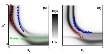
We show the results of our fitting procedure in Fig. 2. In this figure, we compare calculated surface and bulk spectral functions at the Fermi energy with the surface and bulk spectral functions measured by ARPES. The calculations are in good agreement with the experiments, which suggests that the assumptions made in developing our model are reasonable.
III Results and Discussion
III.1 Self-consistent potential, charge density, and superconducting order parameter
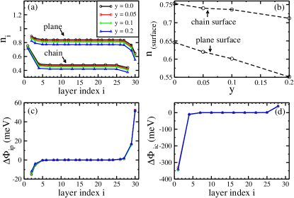
Figure 3 shows the results of self-consistent calculations for the charge density and electrostatic potential. We take the specific case of Y1-yCayBa2Cu3O6.92, which corresponds to optimal doping when and to overdoping when . The self-consistently determined charge density is shown in Fig. 3(a) as a function of layer index . (Recall that the layer indices and label the CuO chain-terminated and the CuO2 plane-terminated surfaces respectively.) As discussed in the introduction, Fig. 3(a) shows that there is charge transfer from the plane-terminated surface to the chain-terminated surface. This charge screens the electric field produced by the polar unit cells, so that the electric potential is constant across the thin film except near the surfaces. This is shown in Fig. 3(c) and (d). In these figures, we have plotted the difference
| (13) |
between the potential in layer and the potential for a plane (chain) in the bulk in order to make the comparison between different values simpler. is nonzero within a screening length of the surfaces and is positive (negative) at the plane (chain) surface. The charge density on the plane (chain) surface is correspondingly smaller (larger) than in the bulk as shown in Fig. 3(a).
We note that , the potential shift at the chain-terminated surface, is roughly seven times larger than , the potential shift at the plane-terminated surface. This ratio is approximately the same as the ratio of the plane and chain densities of states (in the normal state); because of the small density of states in the chains, a large chemical potential shift is required at the chain-terminated surface to accommodate the charge transferred from the plane-terminated surface.
Figure 3 also shows the effect of Ca substitution. Despite the proximity of the Ca ions to the CuO2 layers, changes by roughly the same amount in both the CuO2 and CuO layers. The one notable exception to this is at the chain surface, where the electron concentration changes by roughly half as much as in the bulk [Fig. 3(b)].
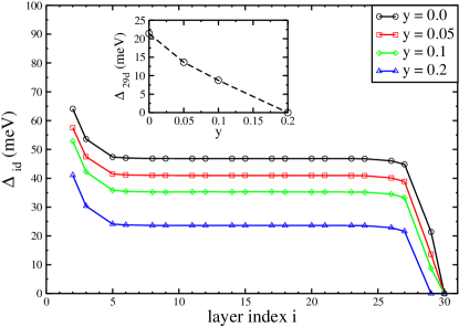
Figure 4 shows the -wave superconducting order parameter as a function of layer index in the CuO2 plane layers, and for different levels of Ca doping. Because is calculated phenomenologically from Eq. (6), it follows . Thus, is larger than in the bulk near the chain surface and smaller than in the bulk near the plane surface. In our calculations, actually vanishes at the CuO2 surface layer (), although there is a spectral gap due to proximity coupling to the subsurface layers. Note that recent ARPES experiments,Zabolotnyy et al. (2007); Nakayama et al. (2007) found that the surface is nonsuperconducting, but tunneling experimentsValles et al. (1991); Maggio-Aprile et al. (1995); Yeh et al. (2001); Ngai et al. (2007); Das et al. (2008); Beyer et al. (2009); Fischer et al. (2007) found a clear superconducting gap at the surface. We will show in the next section that the size of the superconducting gap at the CuO2 surface is sensitive to how the surface is prepared.
III.2 Density of states and spectral function
The main results reported in this work are for the layer-dependent density of states and spectral function. The density of states at energy in layer is given by
| (14) |
where is the total number of -points, and is spectral function in layer ,
| (15) | |||||
Note that the eigenstates and eigenenergies describe electrons () or holes () depending on the spin index. In this work, all results for are shown for the normal state at , while results for are shown in the superconducting state.
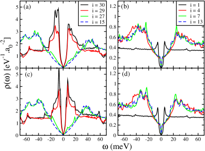
Results for Y1-yCayBa2Cu3O6.92 with and are shown in Fig. 5. This figure shows that the density of states at the surfaces is very different from in the bulk, for both the CuO2 planes and CuO chains. Notably, the -wave gap is significantly smaller at the surfaces than in the bulk. In the CuO2 layers, this reflects the suppression of near the surface due to the decreased electron density in the surface layers. This is consistent with bulk-sensitive ARPES experiments that found a gap of order 42 meV,Okawa et al. (2009) and surface-sensitive tunneling experiments, which consistently find that the gap is meV.Valles et al. (1991); Maggio-Aprile et al. (1995); Yeh et al. (2001); Ngai et al. (2007); Das et al. (2008); Beyer et al. (2009); Fischer et al. (2007) In the chain layers, the reduced gap at the surface reflects the reduced proximity coupling at the chain surface, in part because the chain has only one nearest neighbor CuO2 plane. Our calculation shows that the DOS obtains its bulk value within a few layers of either surface.
We note that, relative to the conventional model of a single-layer -wave superconductor, the DOS in Fig. 5 shows a lot of structure. In particular, the CuO2 surface (for ) has a main gap of about 10 meV, whose coherence peaks are split into pairs of closely-spaced peaks, and a satellite “shoulder” at about 20 meV. Shoulder features have been commonly observed in tunneling experiments, and have been attributed to pairing,Ngai et al. (2007) and to competing order.Beyer et al. (2009) In our calculations, this structure comes from the interplay of pairing and band structure effects, namely the mixing of chain and plane states resulting in an orthorhombic distortion of the Fermi surfaces. This is illustrated in Fig. 6, which shows the layer-resolved spectral function at the Fermi energy. We see from this figure that chain-plane coupling strongly distorts the Fermi surfaces in the region of the Brillouin zone. This distortion is particularly important for the CuO2 layers, because there is a van Hove singularity near the point in the undistorted spectrum. The DOS is therefore sensitive to small changes in the Fermi surface shape, caused either by chain-plane coupling, by doping, or by band-bending (changes in the electrostatic potential) near the surfaces. Thus, the addition of 5% Ca changes the electron density by only electrons per CuO2 plaquette but qualitatively changes the shape of the coherence peaks [compare Fig. 5(a) and (c)]; in Fig. 6, we see that the main effect on the CuO2 surface layer () is indeed near the point, where the spectral weight is reduced by Ca doping.
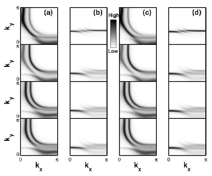
In Fig. 6, the intensity of strongly depends on the amount of hybridization between chain and plane states. The Fermi surface at the CuO-terminated surface () is relatively undistorted, indicating weak chain-plane coupling. By contrast, the chain Fermi surface in the bulk is more strongly hybridized to the CuO2 plane states and is correspondingly washed out. This is a possible reason that the chain Fermi surface was imaged in surface-sensitive ARPES measurementsZabolotnyy et al. (2007); Nakayama et al. (2007) but not in bulk-sensitive measurements.Okawa et al. (2009)
We remark that the amount of hybridization between chains and planes is strongly -dependent, even though the matrix element is independent of . This is because the hybridization at each depends on the energy difference between the chain and plane bands at that value of . Because these bands have different symmetries, the energy difference (and thus the hybridization) is a strong function of . It follows that the amount of hybridization at is a strong function of the relative positions of chain and plane Fermi surfaces, with the hybridization being largest where the Fermi surfaces cross. This explains the difference between the surface () and bulk () spectral functions shown in Fig. 6. A more extensive discussion of this point can be found in Ref. Atkinson, 1999.
The degree to which the chain and plane Fermi surfaces hybridize determines the size of the induced gap in the chain layers. The small gap at the CuO surface (Fig. 5) is thus due to the weak hybridization of the surfaces chains with the underlying CuO2 planes. In the bulk, the chain DOS shown in Fig. 5 has a main gap of about 20 meV, and a small gap of about 4 meV. The small gap originates from sections of the chain Fermi surface that are only weakly coupled to the planes (namely, ) while the large gap comes from sections of the Fermi surface that are strongly coupled to the planes (). The small gap was discussed previously as a possible source for the subgap structure measured in some tunneling experiments.Ngai et al. (2007)
Having discussed general features of the DOS and spectral function, we now discuss how these are affected by changes in specific model parameters. First, we allow for the possibility that the surface layers of the YBCO thin film are doped by the adsorption of atoms or molecules onto the surfaces. Adsorption happens naturally, for example, when YBCO is exposed to air, and deliberate potassium adsorption has been used to control the electron concentration in CuO2 surface states.Hossain et al. (2008) In this work, we are interested in the possibility that the adsorbate layers partially screen the electric fields at the YBCO surfaces. We model this by assuming that the adsorbed layer has an average charge density of () at the CuO2 (CuO) surface, where . In our self-consistent calculations, the effect of the adsorbate charge is to reduce the charge transfer between the chain and plane surfaces.
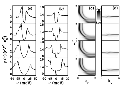
Figure 7 shows the effect of on the density of states and spectral function. We see that even a relatively small adsorbate charge density has a significant effect on both and at the surfaces. In particular, and at the surfaces are increasingly similar to the bulk as increases. This follows directly from the fact that the charge densities at the surfaces approach their bulk values as increases. In the CuO2 layers, this results in a larger from Eq. (6), while in the CuO layers, this results in an increased hybridization between the surface chains and the adjacent CuO2 plane.
The CuO2 spectrum for shown in Fig. 7 is consistent with existing tunneling experiments on optimally-doped YBCO. For this case, we obtain coherence peaks at the CuO2 surface at meV and a satellite peak at meV, in approximate agreement with Refs. Maggio-Aprile et al., 1995; Cren et al., 2000a; Beyer et al., 2009 (when comparing with experiments, recall that a peak at negative energy in the DOS corresponds to a peak at positive voltage bias in a tunneling experiment). We note that having a charged adsorbate layer is not the only way to obtain agreement with experiments; a different value for the dielectric constant, for example, will affect the surface charge density, and consequently the DOS. Whether or not our model is correct in all details, it demonstrates that existing tunneling measurements on optimally-doped YBCO can be explained within a band picture.
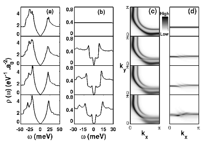
Throughout this work, we have assumed that the plane-chain coupling parameter is meV. This is the hardest of the model parameters to establish, and was chosen because it gives reasonable results for and . Figure 8 shows the effect of varying on the density of states and spectral function. Not surprisingly, chain-plane coupling has little effect on the DOS at the CuO2 surface, apart from a shift of a weak negative-energy satellite peak away from the Fermi energy with increasing . In contrast, the chain surface is strongly influenced by coupling to the CuO2 layer; the CuO chains are metallic when , and an induced gap appears when is nonzero. The induced gap grows approximately linearly with and has both a subgap and a main gap, as discussed earlier. The spectral function also changes with increasing , becoming increasingly distorted near .

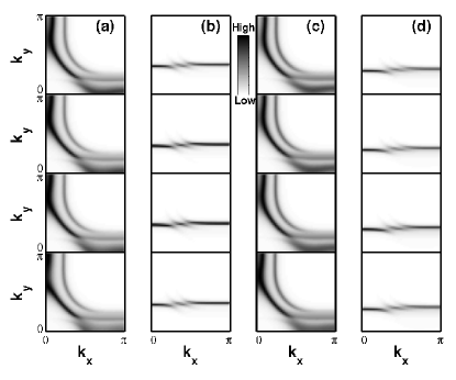
Finally, we look more closely at the effects of Ca doping. In Ngai et al,Ngai et al. (2007) samples with up to 20% Ca substitution for Y were studied, while in Yeh et alYeh et al. (2001), 30% Ca-doped samples were studied. In Fig. 9, we show a series of calculations for the surface DOS of a Y1-yCayBa2Cu3O6.92 thin film. Results are shown for both and . The corresponding spectral functions are shown in Fig. 10.
As discussed above, the DOS exhibits subgap, main gap, and satellite features. In Ngai et al, the three features were attributed to superconductivity on different regions of the Fermi surface. This is generally consistent with our findings here although we have found it difficult to attribute some satellite peaks to specific Fermi surface elements. Experimentally, the ratio between the satellite, main gap, and subgap energies was found to be approximately constant as a function of Ca doping, and this was argued to show that there is a common pairing mechanism for all three features. In our model the energies of the satellite and subgap features in Fig. 9 also scale with the main gap.
In some cases, our calculations reproduce the detailed structure of the experimental spectra. For , Ngai et al showed two types of spectrum. The first is remarkably similar to that shown for in Fig. 9(c), having pronounced coherence peaks and satellite features resembling shoulders. Spectra of this type are also measured in optimally-doped () samples.Maggio-Aprile et al. (1995); Ngai et al. (2007); Cren et al. (2000a); Beyer et al. (2009) The good agreement between our calculations and the measured spectra suggests that our model captures the essential physics of the surface states in optimally-doped YBCO.
The second type of measured spectrum qualitatively resembles that shown for in Fig. 9(d), having weak coherence peaks, a subgap feature, and satellite peaks (indicated by arrows in Fig. 9). However, there is a discrepancy between our calculations and the experiments; at higher Ca doping levels, the measured spectra continue to exhibit three sets of peaks while the satellite peaks in our calculations become less prominent. Given the sensitivity of the DOS to small changes in the model parameters, it is plausible that this discrepancy can be corrected by small changes to the model. It is also possible that extrinsic effects not considered here, for example tunneling matrix elements that emphasize the and regions of the Brillouin zone,Martin et al. (2002); Nieminen et al. (2009) could increase the prominence of the satellite features in tunneling experiments. However, we also cannot rule out the possibility that our simple model for Ca substitution is overly naïve.
Another feature of the DOS that is not explained by our model is the large residual DOS measured experimentally; the DOS is never seen to vanish at in the superconducting state, and is often 50% of the normal state DOS. It is not clear whether the residual DOS is intrinsic (for example, due to pair breaking at the surface) or extrinsic (coming from surface states in an adsorbate layer). It is possible that a full description of the YBCO surface states will require a proper accounting of this residual DOS.
IV conclusions
We have studied the surface and bulk states of Y1-yCayBa2Cu3O6.92 with within a tight-binding model. The model parameters for the CuO2 planes are extracted from photoemission experiments, and self-consistent calculations are used to relate the surface and bulk states. We have calculated the density of states and spectral function as functions of adsorbed surface charge density, chain-plane coupling, and Ca doping. Our main findings are that
-
•
our model produces results which are in simultaneous agreement with surface and bulk ARPES measurements. This supports two key assumptions of the model, that the surface and bulk bands are connected by a simple chemical potential shift and that the Coulomb potential can be treated in a planar approximation.
-
•
the DOS in optimally-doped YBCO can be quantitatively explained by our model. In particular, shoulders measured in the density of states that were previously attributed to pairing or to competing order are found to be band structure effects.
-
•
the superconducting DOS is sensitive to small changes in the model parameters. This suggests that, in materials with CuO chains, small changes in doping of the surface states can have a qualitative effect on the density of states, purely as a result of changes to the band structure. This should be contrasted with BSCCO where it is believed that the doping dependence of the DOS is primarily due to strong correlations.
-
•
we can understand some features of Ca-doped YBCO; for example, our calculations find densities of states at the chain surface with subgap, main gap, and satellite features similar to experiments. However, we have not understood the dependence of this spectrum on Ca concentration.
Acknowledgments
We would like to acknowledge helpful coversations with J. Mannhart, T. Kopp, J. Wei, and J. Ngai. K.P. thanks The Commission on Higher Education Grant, Thailand (Grant No.12/2548) for financial support. This work was supported by NSERC of Canada and by SFB 484 from the DFG. This work was, in part, made possible by the facilities of the Shared Hierarchical Academic Research Computing Network (SHARCNET:www.sharcnet.ca) and Compute/Calcul Canada.
References
- Valles et al. (1991) J. M. Valles, R. C. Dynes, A. M. Cucolo, M. Gurvitch, L. F. Schneemeyer, J. P. Garno, and J. V. Waszczak, Phys. Rev. B 44, 11986 (1991).
- Maggio-Aprile et al. (1995) I. Maggio-Aprile, C. Renner, A. Erb, E. Walker, and O. Fischer, Phys. Rev. Lett. 75, 2754 (1995).
- Yeh et al. (2001) N.-C. Yeh, C.-T. Chen, G. Hammerl, J. Mannhart, A. Schmehl, C. W. Schneider, R. R. Schulz, S. Tajima, K. Yoshida, D. Garrigus, et al., Phys. Rev. Lett. 87, 087003 (2001).
- Ngai et al. (2007) J. H. Ngai, W. A. Atkinson, and J. Y. T. Wei, Phys. Rev. Lett. 98, 177003 (pages 4) (2007).
- Das et al. (2008) P. Das, M. R. Koblischka, H. Rosner, T. Wolf, and U. Hartmann, Physical Review B (Condensed Matter and Materials Physics) 78, 214505 (pages 5) (2008).
- Beyer et al. (2009) A. D. Beyer, M. S. Grinolds, M. L. Teague, S. Tajima, and N.-C. Yeh, EPL 87, 37005 (2009).
- Fischer et al. (2007) O. Fischer, M. Kugler, I. Maggio-Aprile, C. Berthod, and C. Renner, Reviews of Modern Physics 79, 353 (pages 67) (2007).
- Cren et al. (2000a) T. Cren, D. Roditchev, W. Sacks, and J. Klein, EPL (Europhysics Letters) 52, 203 (2000a).
- Beyer et al. (2008) A. Beyer, C.-T. Chen, M. Grinolds, M. Teague, and N.-C. Yeh, Physica C: Superconductivity 468, 471 (2008), ISSN 0921-4534.
- Cren et al. (2000b) T. Cren, D. Roditchev, W. Sacks, J. Klein, J.-B. Moussy, C. Deville-Cavellin, and M. Laguës, Phys. Rev. Lett. 84, 147 (2000b).
- Pan et al. (2001) S. H. Pan, J. P. O’Neal, R. L. Badzey, , C. Chamon, H. Ding, J. R. Engelbrecht, Z. Wang, H. Eisaki, S. Uchida, et al., Nature 413, 282 (2001).
- Howald et al. (2001) C. Howald, P. Fournier, and A. Kapitulnik, Phys. Rev. B 64, 100504 (2001).
- Norman et al. (1995) M. R. Norman, M. Randeria, H. Ding, and J. C. Campuzano, Phys. Rev. B 52, 615 (1995).
- Markiewicz et al. (2005) R. S. Markiewicz, S. Sahrakorpi, M. Lindroos, H. Lin, and A. Bansil, Phys. Rev. B 72, 054519 (pages 13) (2005).
- Yusof et al. (1998) Z. Yusof, J. F. Zasadzinski, L. Coffey, and N. Miyakawa, Phys. Rev. B 58, 514 (1998).
- Hoogenboom et al. (2003) B. W. Hoogenboom, C. Berthod, M. Peter, O. Fischer, and A. A. Kordyuk, Phys. Rev. B 67, 224502 (2003).
- Nakagawa et al. (2006) N. Nakagawa, H. Y. Hwang, and D. A. Muller, Nat. Mater. 5, 204 (2006).
- Thiel et al. (2006) S. Thiel, G. Hammerl, A. Schmehl, C. W. Schneider, and J. Mannhart, Science 313, 1942 (2006).
- Nakayama et al. (2007) K. Nakayama, T. Sato, K. Terashima, H. Matsui, T. Takahashi, M. Kubota, K. Ono, T. Nishizaki, Y. Takahashi, and N. Kobayashi, Phys. Rev. B 75, 014513 (pages 7) (2007).
- Zabolotnyy et al. (2007) V. B. Zabolotnyy, S. V. Borisenko, A. A. Kordyuk, J. Geck, D. S. Inosov, A. Koitzsch, J. Fink, M. Knupfer, B. Büchner, S.-L. Drechsler, et al., Phys. Rev. B 76, 064519 (pages 6) (2007).
- Atkinson and Carbotte (1997) W. A. Atkinson and J. P. Carbotte, Phys. Rev. B 55, 3230 (1997).
- Atkinson and Sonier (2008) W. A. Atkinson and J. E. Sonier, Phys. Rev. B 77, 024514 (pages 8) (2008).
- Whelan and Carbotte (2000) N. D. Whelan and J. P. Carbotte, Phys. Rev. B 62, 15221 (2000).
- Schabel et al. (1998a) M. C. Schabel, C.-H. Park, A. Matsuura, Z.-X. Shen, D. A. Bonn, R. Liang, and W. N. Hardy, Phys. Rev. B 57, 6090 (1998a).
- Schabel et al. (1998b) M. C. Schabel, C.-H. Park, A. Matsuura, Z.-X. Shen, D. A. Bonn, R. Liang, and W. N. Hardy, Phys. Rev. B 57, 6107 (1998b).
- Lu et al. (2001) D. H. Lu, D. L. Feng, N. P. Armitage, K. M. Shen, A. Damascelli, C. Kim, F. Ronning, Z.-X. Shen, D. A. Bonn, R. Liang, et al., Phys. Rev. Lett. 86, 4370 (2001).
- Kondo et al. (2007) T. Kondo, R. Khasanov, J. Karpinski, S. M. Kazakov, N. D. Zhigadlo, T. Ohta, H. M. Fretwell, A. D. Palczewski, J. D. Koll, J. Mesot, et al., Physical Review Letters 98, 157002 (pages 4) (2007).
- Okawa et al. (2009) M. Okawa, K. Ishizaka, H. Uchiyama, H. Tadatomo, T. Masui, S. Tajima, X.-Y. Wang, C.-T. Chen, S. Watanabe, A. Chainani, et al., Physical Review B (Condensed Matter and Materials Physics) 79, 144528 (pages 9) (2009).
- Tachiki et al. (1990) M. Tachiki, S. Takahashi, F. Steglich, and H. Adrian, Z. Phys. B Cond. Mat. 80, 161 (1990).
- O’Donovan and Carbotte (1997) C. O’Donovan and J. P. Carbotte, Phys. Rev. B 55, 1200 (1997).
- Atkinson (1999) W. A. Atkinson, Phys. Rev. B 59, 3377 (1999).
- Morr and Balatsky (2001) D. K. Morr and A. V. Balatsky, Phys. Rev. Lett. 87, 247002 (2001).
- Andersen et al. (1995) O. K. Andersen, A. I. Liechtenstein, O. Jepsen, and F. Paulsen, J. Phys. Chem. Solids 56, 1573 (1995).
- Ye and Li (2007) X.-S. Ye and J.-X. Li, Phys. Rev. B 76, 174503 (pages 6) (2007).
- Smilde et al. (2005) H. J. H. Smilde, A. A. Golubov, Ariando, G. Rijnders, J. M. Dekkers, S. Harkema, D. H. A. Blank, H. Rogalla, and H. Hilgenkamp, Phys. Rev. Lett. 95, 257001 (pages 4) (2005).
- Böttger et al. (1996) G. Böttger, I. Mangelschots, E. Kaldis, P. Fischer, C. Krüger, and F. Fauth, Journal of Physics: Condensed Matter 8, 8889 (1996).
- Hossain et al. (2008) M. A. Hossain, J. D. F. Mottershead, D. Fournier, A. Bostwick, J. L. McChesney, E. Rotenberg, R. Liang, W. N. Hardy, G. A. Sawatzky, J. S. Elfimov, et al., Nat. Phys. 4, 527 (2008).
- Martin et al. (2002) I. Martin, A. V. Balatsky, and J. Zaanen, Phys. Rev. Lett. 88, 097003 (2002).
- Nieminen et al. (2009) J. Nieminen, H. Lin, R. S. Markiewicz, and A. Bansil, Phys. Rev. Lett. 102, 037001 (pages 4) (2009).