Investigation of the Photocurrent in Bulk Heterojunction Solar Cells
Abstract
We investigated the photocurrent in poly(3-hexylthiophene-2,5-diyl) (P3HT):[6,6]-phenyl-C61 butyric acid methyl ester (PCBM) solar cells by applying a pulsed measurement technique. For annealed samples, a point of optimal symmetry (POS) with a corresponding voltage of 0.52–0.64 V could be determined. Based on macroscopic simulations and results from capacitance–voltage measurements, we identify this voltage with flat band conditions in the bulk of the cell, but not the built-in voltage as proposed by [Ooi et al., J. Mater. Chem. 18 (2008) 1644]. We calculated the field dependent polaron pair dissociation after Onsager–Braun and the voltage dependent extraction of charge carriers after Sokel and Hughes with respect to this point of symmetry. Our analysis allows to explain the experimental photocurrent in both forward and reverse directions. Also, we observed a voltage–independent offset of the photocurrent. As this offset is crucial for the device performance, we investigated its dependence on cathode material and thermal treatment. From our considerations we gain new insight into the photocurrent‘s voltage dependence and the limitations of device efficiency.
pacs:
71.23.An, 72.20.Jv, 72.80.Le, 73.50.Pz, 73.63.BdI Introduction
Organic solar cells have improved greatly in the last years, reaching 5–6 % power conversion efficiency (PCE) today.Park2009 However, the Shockley diode equation cannot explain the voltage dependent photocurrent in organic solar cells based on a physical model. schilinsky2004 The detailed process leading from photoinduced polaron pairs to extracted charge carriers and external photocurrent needs better understanding to push development of these devices systematically.deibel2009c The first step in this process is singlet exciton formation upon absorption of a photon, usually on the polymer. Then, the exciton has to diffuse to a polymer-fullerene interface within its lifetime, where, due to the high electron affinity of the fullerene, a polaron pair is created via ultrafast charge-transfer.sariciftci1992 These polaron pairs are still Coulomb-bound due to a low dielectric constant of the organic material system (typically 3–4), and have to be dissociated to free polarons. Provided the free polarons arrive at their respective electrodes, the last step is charge extraction.
In this paper, we investigate the symmetry and voltage dependence of the photocurrent, and compare this to a model that takes field dependent polaron pair dissociation and voltage dependent charge extraction into account. The photocurrent , defined as the difference of illuminated and dark current, , can experimentally be accessed using pulsed illumination (inset in Figure 1). This is necessary to avoid a major overestimation due to device heating.ooi2008
We find the photocurrent of annealed P3HT:PCBM solar cells to have a point of optimal symmetry (POS). The photocurrent shows a point symmetry with respect to POS (see Figure 1), and the corresponding voltage is in the range of 0.52–0.64 V. While these values agree with results of Ooi et al.ooi2008 , our interpretation differs. We identify this voltage as the quasi flat band case–with flat bands in the bulk of the solar cell–which is well below the built-in voltage. Accordingly, our considerations lead to new insights into the origin of the photocurrent.
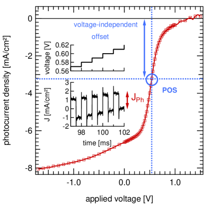
As shown in Figure 1, the photocurrent is composed of two contributions. The first is voltage-dependent and symmetric with respect to POS. The second contribution is a voltage-independent offset. This constant offset is usually negative, thereby increasing the short-circuit current and PCE. As the magnitude of this offset is crucial for device performance, we investigated its dependence on thermal treatment, cathode material and active layer thickness in detail.
In order to describe the voltage dependence of , we use a combination of Braun–Onsager braun1984 ; onsager1938 theory and charge extraction as calculated by Sokel and Hughes. sokel1982 This combination was proposed by Mihailetchi et al. mihailetchi2004a and could for the first time explain the experimental photocurrent in reverse direction. However, they calculated effective voltage and field with respect to the physically ill-defined voltage , at which . As we will show, this is correct only in the special case where coincides with . In general, contact effects result in a lower value of . Consequently, we consider voltage and electric field relative to instead of . Calculating polaron pair dissociation and charge extraction with respect to the point of symmetry now allows to describe the experimental photocurrent for solar cells with different electrode material. Using a pulsed measurement technique also makes the photocurrent in forward direction accessible, and shows that the model can describe the data in both directions.
II Experimental
All samples investigated were spin-coated from solution of a 1:1 weight ratio of P3HT and PCBM in chlorobenzene, onto indium tin oxide/glass substrates coated with poly(3,4-ethylenedioxythiophene):poly(styrenesulfonate). After an annealing step at 140 , metal contacts were applied by thermal evaporation; either Ca (3 nm) followed by Al (110 nm) or only Ag (120 nm). All fabrication and characterization took place in a nitrogen atmosphere glovebox. The cells with Ca/Al cathode had fill-factors (FF) of about 60 % and PCE of 2–3 %, as determined with a Xe-lamp, adjusted to simulate standard testing conditions (STC).shrotriya2006
The photocurrent measurements were performed based on the setup proposed by Ooi et al. ooi2008 , using a white 10 W LED for pulsed illumination. The pulse duration was set to 0.5 ms at a duty cycle of 50 %, giving the cell ample time to reach steady-state after switching the light on/off. The illumination level was equivalent to one sun, based on comparison of the short-cuircuit current () reached with the LED to the reached under simulated STC. The active layer thickness was determined with a Veeco Dektak 150 profilometer.
For the capacitance–voltage (CV) measurements we applied a 5 kHz AC voltage with an amplitude of 40 mV to our cells and performed a DC bias sweep. It was carried out under nitrogen atmosphere and without any incident light to the device to prevent distortions due to charge carrier generation. Data acquisition was carried out with an Agilent E4980A LCR-meter in parallel RC circuit mode. The reasonability of this working mode has been proven by preceding impedance measurements that showed a clear semicircle (with a negligible offset impedance of about 10 , corresponding to the series resistance ) in Cole–Cole representation for our cells. Since we have Schottky-like contacts at the metal–semiconductor interfaces of our devices, the value of was determined by the intercept of a linear fit of the Mott–Schottky plot.
All presented simulations were done solving the one dimensional differential equation system of Poisson‘s equation and the continuity equations for electron and holes in a numerical iterative approach,selberherr1984 ; deibel2008a implicitly assuming a band-like transport. A 100 nm thick bulk-heterojunction solar cell is calculated at a temperature of K containing electrons and holes with equal mobilities of cm2/Vs.baumann2008 For the active material, the effective medium approach is used, leading to effective electrical bandgap of eV between the donor HOMO (highest occupied molecular orbital) and the acceptor LUMO (lowest unoccupied molecular orbital) level and an effective dielectric constant of .baumann2008 The effective charge carrier densities of LUMO and HOMO—describing the spatial charge carrier densities of electrons and holes by Fermi-Dirac statistics—were set to cm-3. The interfaces towards the electrodes are assumed to possess injection barriers of 0.1 eV without any surface recombination.rauh2010
Illumination is taken into account by a homogenous charge carrier generation rate over the whole device. This simplification avoids band bending due to local differences of the charge carrier densities caused by optical interference inside the sample. We use Langevin theory to describe bimolecular charge carrier recombination of free polarons to the ground state.langevin1903 The combination of charge carrier generation and recombination leads to the following net generation rate:
| (1) |
with the elementary charge , the dielectric constant , the Boltzmann constant and the intrinsic charge carrier density .
The result of this system are spatially resolved values for the electrical potential and electron and hole densities in form of quasi-Fermi potentials. In order to create a band structure, the potentials have to be transformed into an energy level. Since experimental values of device work functions are not available, the electron conducting contact (here aluminum) is set to a typical value of -4.25 eV,sze1981 which determines the absolute value of all other potentials.
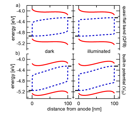
In Figure 2 the resulting band structures are presented in the dark and under illumination for two important bias voltages. First, a voltage resulting in flat bands—and therefore zero electric field , being the spatial derivative of the potential—in the middle of the sample, and second the built-in voltage for comparison.
III Results and Discussion
III.1 Origin of
The photocurrent shows a high symmetry with respect to POS, with a corresponding voltage in the range of 0.52–0.64 V for annealed solar cells with Ca/Al cathode under 1 sun. This agrees with findings of Ooi et al.,ooi2008 who reported a of 0.58–0.60 V for cells with Al cathode.
To understand this symmetry in , we look at the energy bands in the solar cell. Due to the band bending at the contacts, a case of flat bands in the whole device does not exist. However, our macroscopic simulation shows flat band conditions with zero electric field in the bulk of the cell at an applied voltage of 0.66 V (Figure 2a). We call this the quasi flat band (QFB) case, which is well below the built-in voltage at 0.90 V (Figure 2b).
The reason why the bias must be reduced from in order to achieve flat bands in the bulk is the band bending at the electrodes, which is a consequence of the boundary conditions for the quasi-Fermi levels at the interfaces. Ideally, the electrodes inject charge carriers of one type into the organic semiconductor and extract the other type. This generates a strong diffusive current in the contact region which is, in thermal equilibrium, accompanied by a high electric field in the opposite direction, especially next to the electrodes. As shown in Figure 2, the resulting band bending is almost independent of illumination. Only the quasi-Fermi levels are affected, indicating a higher charge carrier density under illumination.
This reduced voltage was published by Kemerink et al., but incorrectly identified as .kemerink2006 At QFB, the electric field is zero in the bulk of the solar cell and finite in vicinity of the contacts, while at the field is finite at every position in the cell.
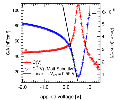
Capacitance–voltage measurements—conducted in the dark—further support the interpretation of being the quasi flat band case. The capacitance (where is the electric charge) depends on the differential variation of the electric field in the bulk, which approaches zero in this case whereby the capacitance approaches infinity. An extrapolation of to zero (linear fit to the Mott–Schottky plot, see Figure 3) yields , which therefore corresponds to the quasi flat band voltage. This is a common technique to determine the flat band voltage in inorganic semicondutors, blood but has already been applied to organic devices.yakuphanoglu2008 ; bisquert2008 We found to be 0.5–0.6 V, which agrees with the observed values for .
The quasi flat band case is distinct and can explain the symmetry of the photocurrent. Energy bands with zero slope present a special, symmetric situation, as a relative bias in either direction will cause the photogenerated carriers in the bulk to flow equally strong, but in different directions. In conclusion of this, we propose to correspond to the case of flat bands in the bulk of the active layer, with finite electric field in vicinity of the contacts, caused by band bending due to injection barriers. Hence, the electric field in the bulk will be proportional to an effective voltage . In contrast to Ooi et al., ooi2008 we do not assume to equal the built-in voltage , but to be considerably smaller.
III.2 Voltage-independent offset of
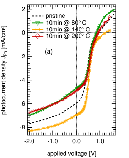
As mentioned above, the photocurrent is composed of two contributions. The first is voltage-dependent and symmetric with respect to POS. The second contribution is a voltage-independent offset, which is crucial for device performance and can be influenced by processing parameters. Figure 4 shows the influence of cathode material and annealing conditions on the photocurrent. While the shape of remains similar, the offset is critically dependent on both cathode material and thermal treatment. With respect to the pristine sample, the offset decreases after thermal treatment at 80 or 200 , but increases upon treatment at 140 (Figure 4a). Using Ag as cathode material yields a much smaller offset than Ca/Al, while the shape of the photocurrent curves is very similar (Figure 4b). is also smaller for cells with Ag cathode, with values of about 0.45 V, which is a direct consequence of the higher injection barriers. Active layer thickness influences the magnitude of the offset as well. The highest negative offset, up to 4.1 , was observed for solar cells with Ca/Al cathode, active layer thickness of 120 nm and thermal annealing at 140 . These cells had the highest and PCE.
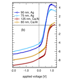
As this voltage-independent offset can be influenced by the choice of cathode material without changing the shape of the photocurrent significantly, we assume the contact regions to be responsible for the offset. The voltage dependent part of then corresponds to the photocurrent generated in the bulk of the solar cell.
Ooi et al. explained this offset with self-selective electrodes,ooi2008 resulting in a constant diffusion current , where is the elementary charge, the diffusivity and the concentration of photogenerated charge carriers at the selective electrode. In contrast to this predicted dependence, we observed a maximum (negative) offset for a thickness of about 120 nm, with smaller offsets for thinner and thicker devices (not shown).
As an alternative explanation for this constant offset, we propose the band bending in vicinity of the contacts, which—independently of applied bias—has only one direction and results in an electric field high enough for efficient polaron pair dissociation (see Figure 2). The contact regions would then give a constant contribution to , which depends on the degree of band bending—and therefore the height of the injections barriers—while the bulk region contributes to as a function of applied voltage and causes the symmetry.
The exact nature of this offset and its dependence on the cathode material has to be further investigated. A highly negative offset is crucial for device performance, and should be optimized, e.g. by choice of cathode material.
III.3 Voltage vs. field dependence
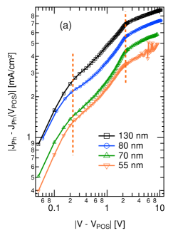
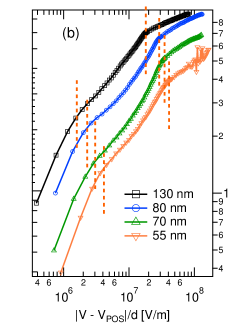
The active layer thickness has only little influence on the voltage dependence of the observed photocurrent (Figure 5(a)). Of course the absolute value of is higher for thicker cells, but the shape of is very similar for cells with thicknesses between 55 and 130 nm. This is surprising, since e.g. polaron pair dissociation and thereby are supposed to be dependent on electric field .deibel2009 In the simplest approximation, assuming a constant slope in energy bands over the whole extension of the device, the effective field is the fraction of effective voltage and active layer thickness:
| (2) |
Characteristic points of the photocurrent, indicated by red dashed lines in Figure 5, lie on top of each other when plotted against effective voltage . When plotted against the calculated field (Equation (2)), the curves of disperse (Figure 5(b)). This indicates that the approximation for the internal field in Equation (2) is not realistic. The reason for this is the voltage drop at the contacts (Figure 2), which greatly reduces the electric field in the bulk of the cell. In addition the photocurrent is not only governed by field dependent polaron pair dissociation, but also depends on the extraction of charge carriers. As described below, the active layer thickness does not influence this extraction mechanism.
III.4 Polaron pair dissociation and charge extraction
To describe the voltage dependence of the photocurrent, we propose a model that takes field-dependent polaron pair (PP) dissociation and voltage dependent polaron extraction by drift and diffusion into account. A well-known model to describe field-dependent PP dissociation was presented by Braun in 1984.braun1984 Using the field dependence for ion-pair dissociation by Onsager and Langevin recombination for polarons,onsager1938 ; langevin1903 Braun derives the following PP dissociation probability:
| (3) |
where is the PP dissociation rate. It can be calculated by detailed balance from the recombination rate and the Coulomb binding energy, which depends on the PP radius . is the decay rate of a PP to the ground state. Since and do not influence independently, we use their product as a single parameter. deibel2009
Upon successful separation, the polarons need to travel to the electrodes to be extracted. This part can be described with a term introduced by Sokel and Hughes.sokel1982 They solved the problem of photoconductivity in insulators analytically, neglecting dark current, trapping and recombination. The negligence of recombination is a resonable approximation.pivrikas2005 ; deibel2008b ; deibel2009prb The result depends on temperature and applied voltage :
| (4) |
Using an effective voltage and a calculated field , and adding the constant offset , the overall photocurrent can be written as:
| (5) |
This combination of Braun-model for polaron pair dissociation and the Sokel–Hughes term for charge extraction was first proposed by Mihailetchi et al.,mihailetchi2004a but with the assumption that . This corresponds to the special case of a vanishing offset, where equals . Also, they used a Gaussian distribution of polaron pair radii to calculate the dissociation efficiency in the Braun model. While this assumption seems reasonable, a fixed value for could describe our data better than a distributed one.
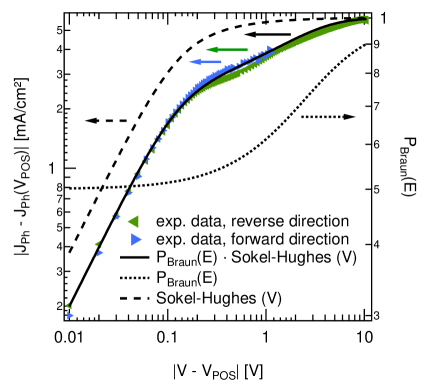
As shown in Figure 6, the product of PP dissociation after Braun and extraction after Sokel–Hughes (Equation (5)) describes the experimental photocurrent well in both forward and reverse directions. A set of parameters in a narrow range could be employed to describe the experimental photocurrent of solar cells with different active layer thickness and cathode material over the whole measured range (Figure 7).
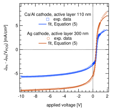
Using Equation (2) to calculate , effective values of about 400 nm for were used in the model, almost independent of measured device thickness and clearly exceeding it. This is a consequence of the voltage drops at the contacts (Figure 2). Low injection barriers result in a high band bending in vicinity of the electrodes and reduced electric field in the bulk of the cell, corresponding to a seemingly greater . The approximation is therefore flawed.
The saturated, voltage-dependent part of the photocurrent is typically 5–8 , with higher values for thicker cells. The dielectric constant was set to 3.5 and temperature to 310 K (slightly above room temperature to account for heating under illumination). The product of spatially averaged mobility and PP lifetime (with respect to the ground state) was set to 1–3 and the PP radius to 1.8–2.0 nm.
Using this parameter set, the dissociation efficiency of polaron pairs in the bulk can be calculated to be 40–60 % at zero field. However, extraction is the limiting factor at low effective voltages. Only at higher effective voltages, the field dependence of polaron pair dissociation determines the shape of the photocurrent.
IV Conclusions
By use of a pulsed measurement technique, we find a point of symmetry for the photocurrent at 0.52–0.64 V in P3HT:PCBM organic solar cells, which agrees with results from capacitance–voltage measurements. Based on our macroscopic simulation, we identify this voltage as the point of flat bands in the bulk of the solar cell, the quasi flat band case, well below the built-in potential. We find a voltage-independent offset of the photocurrent, which is crucial for high , which depends both on thermal annealing conditions and cathode material. We also propose a possible origin of this offset with the band-bending close to the contacts. Active layer thickness has an influence on this offset, but surprisingly little impact on the shape of .
A model including polaron pair dissociation, based on Braun–Onsager theory, and extraction, based on the work by Sokel & Hughes, can describe our data for different solar cells with a narrow range of parameters. The electric field in the bulk of the cell is greatly reduced by the injection barriers. At zero electric field, polaron pair dissociation efficiency is 40–60 %.
Since the maximum power point is close to , where the effective voltage is zero, the photocurrent under operating conditions is largely determined by the voltage independent offset. For best device performance it is necessary to maximize this constant contribution from the contact regions and simultaneously enhance polaron pair dissociation and polaron extraction in the bulk.
Acknowledgements.
The authors thank the Bundesministerium für Bildung und Forschung for financial support in the framework of the MOPS project (contract no. 13N9867). V.D.’s work at the ZAE Bayern is financed by the Bavarian Ministry of Economic Affairs, Infrastructure, Transport and Technology.References
- (1) S. H. Park, A. Roy, S. Beaupre, S. Cho, N. Coates, J. S. Moon, D. Moses, M. Leclerc, K. Lee, and A. J. Heeger, Nature Photonics 3, 297 (2009)
- (2) P. Schilinsky, C. Waldauf, J. Hauch, and C. J. Brabec, J. Appl. Phys. 95, 2816 (2004)
- (3) C. Deibel, Phys. Stat. Sol. A 206, 2731 (2009)
- (4) N. S. Sariciftci, L. Smilowitz, A. J. Heeger, and F. Wudl, Science 258, 1474 (1992)
- (5) Z. E. Ooi, R. Jin, J. Huang, Y. F. Loo, A. Sellinger, and J. C. deMello, Journal of Materials Chemistry 18, 1644 (2008)
- (6) C. L. Braun, J. Chem. Phys. 80, 4157 (1984)
- (7) L. Onsager, Phys. Rev. 54, 554 (1938)
- (8) R. Sokel and R. C. Hughes, J. Appl. Phys. 53, 7414 (1982)
- (9) V. D. Mihailetchi, L. J. A. Koster, J. C. Hummelen, and P. W. M. Blom, Phys. Rev. Lett. 93, 216601 (2004)
- (10) V. Shrotriya, G. Li, Y. Yao, T. Moriarty, K. Emery, and Y. Yang, Adv. Funct. Mater. 16, 2016 (2006)
- (11) S. Selberherr, Analysis and simulation of semiconductor devices (Springer, 1984)
- (12) C. Deibel, A. Wagenpfahl, and V. Dyakonov, phys. stat. sol. (RRL) 2 4, 175 (2008)
- (13) A. Baumann, J. Lorrmann, C. Deibel, and V. Dyakonov, Appl. Phys. Lett. 93, 252104 (2008)
- (14) D. Rauh, C. Deibel, and V. Dyakonov, unpublished
- (15) P. Langevin, Ann. Chim. Phys. 28, 433 (1903)
- (16) S. M. Sze, Physics of semiconductor devices, Second edition (John Wiley & Sons, Inc., 1981)
- (17) M. Kemerink, J. M. Kramer, H. H. P. Gommans, and R. A. J. Janssen, Appl. Phys. Lett. 88, 192108 (2006)
- (18) P. Blood and J. W. Orton, The Electrical Characterization of Semiconductors: Majority Carriers and Electron States (Techniques of Physics) (Academic Press, 1992)
- (19) F. Yakuphanoglu and B. F. Senkal, Polym. Adv. Technol. 19, 1882 (2008)
- (20) J. Bisquert, G. Garcia-Belmonte, A. Munar, M. Sessolo, A. Soriano, and H. J. Bolink, Chem. Phys. Lett. 465, 57 (2008)
- (21) C. Deibel, T. Strobel, and V. Dyakonov, Phys. Rev. Lett. 103, 036402 (2009)
- (22) A. Pivrikas, R. Österbacka, G. Juška, K. Arlauskas, and H. Stubb, Synth. Met. 155, 242 (2005)
- (23) C. Deibel, A. Baumann, and V. Dyakonov, Appl. Phys. Lett. 93, 163303 (2008)
- (24) C. Deibel, A. Wagenpfahl, and V. Dyakonov, Phys. Rev. B 80, 075203 (2009)