Conductance in Co|Al2O3|Si|Al2O3 Permalloy with asymmetrically doped barrier
Abstract
We report on dependence of conductance and tunnelling magnetoresistance on bias voltage at different temperatures down to 2K in CoAl2O3(10Å)Si()Al2O3(2Å)Permalloy magnetic tunnel junctions. Complementary low frequency noise measurements are used to understand the conductance results. The obtained data indicate the breakdown of the Coulomb blockade for thickness of the asymmetric silicon layer exceeding 1.2Å. The crossover in the conductance, the dependence of the tunnelling magnetoresistance with the bias voltage and the noise below 80K correspond to 1 monolayer coverage. Interestingly, the zero bias magnetoresistance remains nearly unaffected by the presence of the silicon layer. The proposed model uses Larkin-Matveev approximation of tunnelling through a single impurity layer generalized to 3D case and takes into account the variation of the barrier shape with the bias voltage. The main difference is the localization of all the impurity levels within a single atomic layer. In the high thickness case, up to 1.8Å, we have introduced a phenomenological parameter, which reflects the number of single levels on the total density of silicon atoms.
I Introduction
The discovery of large tunnelling magnetoresistance (TMR) at room temperature Moodera et al. (1995); Miyazaki and Tezuka (1995) has strongly renewed the interest in spin tunnelling phenomena. Up to very recently the main efforts were concentrated on the increase of tunnelling magnetoresistance values by using ferromagnetic electrodes with the highest possible spin polarization (half metallic ferromagnetism), searching for new types of insulating barriers (including the so called spin filters LeClair et al. (2002)), or a combination of both approaches, where the ferromagnetic/insulator interface design could also play an important role for spin polarized tunnelling. The last approach has recently provided an enormous progress in the TMR values at room temperatures. It has been demonstrated that in epitaxial Fe/MgO/Fe magnetic tunnel junctions (MTJ), where there exist conditions for coherent propagation of specific spin orbitals from one ferromagnetic electrode to the other one, TMR has reached experimentally values up to 410 Yuasa et al. (2006). This fact, supported by theoretical calculations predicting a TMR of more than 1000 have further increased both the fundamental and technological interest in spin polarized tunnelling.
Another possible research direction, which remains however poorly explored, is related to tunnelling in complex (hybrid) junctions. Indeed, the manipulation of the barrier by doping with magnetic or nonmagnetic impurities, or inserting magnetic, for example see reference Schelp et al. (1997), nonmagnetic Shyu et al. (2003) (even superconducting Takahashi et al. (1999); Shyu et al. (2003)) quantum dots (QD), would add a new degree of freedom to spin polarized tunnelling and strongly enhance the versatility of spintronic devices based on spin polarized tunnelling. Tunnelling in such hybrid, but non magnetic devices, has been intensively studied during the last two decades and especially in single electron transistors where the gate electrode is attached to quantum dots separated by two barriers each with a metallic contact (emitter and collector)Maekawa (2006).
Recent theoretical studies of hybrid spintronic devices with two ferromagnetic leads contacting single or double quantum dots have revealed plenty of new interesting phenomena related with the interplay between magnetic tunnelling processes and spin/charge accumulation on quantum dots. From the experimental side, some few groups have demonstrated that Coulomb interaction may indeed play an important role not only in ferromagnetic granular systems Yakushiji et al. (2002) (as occurs in the corresponding nonmagnetic analogs), but also in ferromagnetic single electron tunnelling devices constructed either from a 2D electron gas Ono et al. (1996) or when a single metallic nanoparticle is contacted by ferromagnetic electrodes Bernand-Mantel et al. (2006). It has also been reported that in ultrasmall nanoparticles, with a diameter between 5-10nm, their electronic structures (i.e. quantum effects) may also influence spin polarized tunnelling Deshmukh and Ralph (2002). Other interesting examples of spin polarized tunnelling in hybrid structures include ferromagnetic leads contacting carbon nanotubes Jensen et al. (2005) or a C60 molecule Pasupathy et al. (2004).
Actually, from the technological point of view, it is easier to attach ferromagnetic leads via tunnelling barriers to an array instead of to a single quantum dot. This method, despite the evident drawback due to some distribution in QD sizes and the corresponding charging energies, adds evident versatility to the design of the experiment, allowing continuous tuning between two different regimes: (i) weak doping regime where QDs are substituted by impurities and (ii) strong doping regime. In the second regime one would expect the QD charging energy to reduce continuously with the average dot size, allowing sequential electron transport through an otherwise blocked channel (Coulomb blockade) in addition to direct tunnelling.
Therefore, the knowledge of different mechanisms affecting the conductance, and especially its dependence on the applied bias, could be an important instrument for a comparative analysis of noise and transport. We should, however, note that the bias dependence of conductivity and TMR in real magnetic tunnel junctions, is still poorly understood. The most accepted model Slonczewski (1989), which does not take into account the possible defects inside the barrier, predicts an attenuation of the polarization due to the decrease of the difference between the height of the barrier and the bias voltage. However, the observed reduction in conductivity usually exceeds the predicted effect.
Two theories have been developed in order to explain the anomalous reduction in TMR. The first one explores the existence of impurity states, which reduce the spin current polarization and influence the conductance of the junctions at low bias Bratkovsky (1997). The second one involves inelastic tunnelling as the main origin of unpolarized current Zhang et al. (1997). This point of view has been also supported by the measurement of inelastic tunnelling in magnetic tunnel junctions Moodera et al. (1998). Later on Ding et al Ding et al. (2003) have also detected a tunnelling magnetoresistance in vacuum based magnetic tunnel junctions with a reduced dependence on the bias voltage. These results indicate a possible influence of the impurity states on the polarization of the tunnel current.
For the nonmagnetic tunnel junctions with (nonmagnetic) nanoparticles inside the barrier the presence of a zero bias anomaly was first reported and explained by Giaever Zeller and Giaever (1969). The main mechanism responsible for the appearance of the threshold voltage is Coulomb blockade, which controls two steps tunnelling. In this model the threshold voltage is distributed from 0 V to a maximum voltage . In the doped tunnel junctions is given by the size of the doping particles, which determines a charging energy, given by the capacitance of the particles. This provides some distribution in the population of electrons inside the particles.
The two steps tunnelling in a magnetic tunnel junction has been later treated using the other method developed by Glazman and Matveev Glazman and Matveev (1988); Larkin and Matveev (1987). This theory states that the current is defined, in each particle, by the tunnelling rates from one of the electrodes to the central particle, and from the island to the other electrode. As soon as conductance and spin current polarization are modified, a modification of the dependence on voltage of the tunnelling magnetoresistance may be expected. Indeed, when the bias voltage is increased, the number of allowed two steps processes is also increased.
Previously to this work, Jansen et al. Jansen and Moodera (2000) studied MTJs with Si nanoparticles up to 1.8Å introduced in a symmetric position. They observed gradual suppression of tunnelling magnetoresistance. In the present work Si particles were introduced asymmetrically inside the barrier. While symmetric doping effectively separates the barrier into two parts with similar tunneling rates, the asymmetric doping is expected to affect weakly the largest tunneling rate minimizing the influence of the nonmagnetic Si doping (at least for relatively weak doping levels).
This work presents an experimental study of electron transport in Co(100Å)/Al2O3(10Å)/Si()/Al2O3(2Å)/Py(100Å) hybrid magnetic tunnel junctions, where the largest barrier is 5 times larger than the short one. We observed a continuous transition between the weak (Si impurities) and strong (array of Si quantum dots) regimes. In order to discriminate the different conductance regimes, we study the temperature and bias dependence of both the conductivity and TMR as a function of Si doping.
II Experimental details.
Details of sample preparation have been published previously Jansen and Moodera (2000). For silicon doped samples, the tunnel barriers were deposited in two steps. After deposition of the underlying Co electrode, a first tunnel barrier was formed by deposition and subsequent oxidation of 10 Å of Al. Subsequently, sub-monolayer amounts of Si ( in the following) were deposited on the Al2O3 surface, followed by a second Al layer deposition (2 Å) and oxidation, resulting in a “-doped” Al2O3|Si|Al2 O3 tunnel barrier. After the deposition of the barrier 100 Å of permalloy were deposited, in order to form the second magnetic layer. All the samples thicknesses were measured using a quartz monitor. The quality of the Al layers and the Al2O3 has been previously tested in Ref. Moodera et al. (1997); Jansen et al. (2000). In the following the positive bias voltage corresponds to the application of the voltage in the top electrode, while the negative to application of the voltage in the bottom one.
Measurements were performed using a computer controlled system Guerrero et al. (2005), which allows to detect the dynamic resistance, the DC value of the current and the voltage, and the noise in the device under study. Biasing of the samples was done at a constant current, applied using a calibrated source. It also allowed to modulate the applied current. A square waveform was used in order to detect the transfer function of the line and the dynamic resistance of the junctions. The voltage response of the devices was amplified by using DC coupled low noise amplifiers. The amplified signal was recorded in an analog-digital converter.
The measurement of the noise uses the same biasing technique and the same low noise amplifiers, which were placed in the top part of a cryostat. The pre-amplified signals are further amplified by additional low-noise amplifiers (Stanford Research SR560). A spectrum analyzer SR780 calculates the cross-correlation spectrum of the voltage noise, containing thermal, shot and contributions. The obtained dynamic resistance allows to convert the voltage noise into the current noise. Extrinsic noise, introduced by the amplifiers and the current source, was removed by using the data extracted from a careful calibration performed on resistors at low temperatures. In the experiments we measured 9 different samples, 2 of each Si thickness, except for =0.6Åwhere we only charaterized 1.
III Conductance, zero bias anomaly and tunnelling magnetoresistance
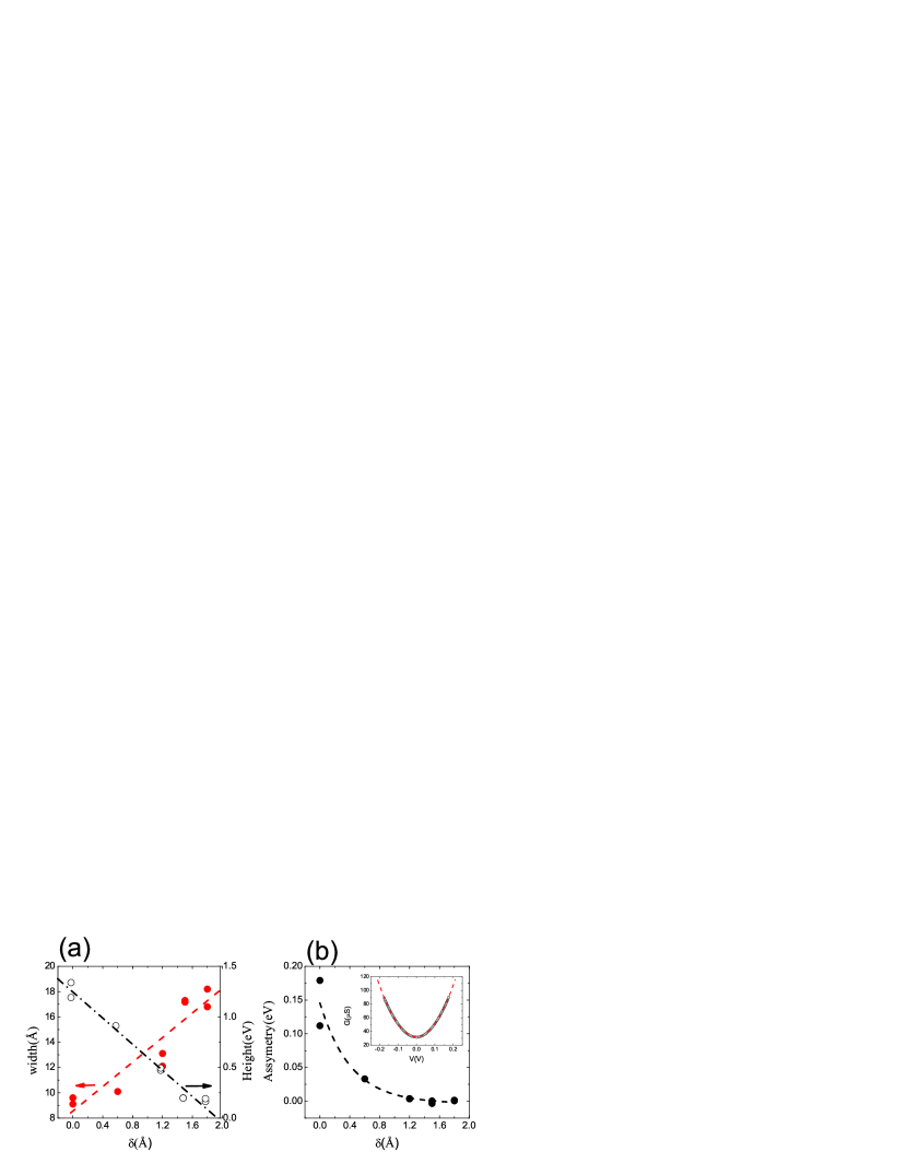
At room temperature the dependence of the conductance on the bias voltage fits well to a parabolic function (see inset to Fig. 1b). The parabolic dependence of the conductance, being due to direct tunnelling, was explained within the Brinkman-Dynes-Rowell (BDR) model Brinkman et al. (1970), which describes the tunnelling conductance as a function of the parameters of a trapezoidal barrier: the width, the average height and the difference between the sides of the barrier, such difference being known as asymmetry.
The results of the fits are plotted in Fig. 1, showing in general an increase of the barrier width with Si doping. However, the increase of the width does not correspond with the deposited Si thickness. As to the height of the barrier, it clearly diminishes when the silicon is introduced inside the barrier. At present we have no clear explanation for this reduction. One of the possible reasons could be some decrease of the work function of the aluminium oxide. This explanation, however, contradicts the observed variation of the barrier asymmetry (Fig. 1), which decreases with the thickness of the Si layer. The disagreement between the deposited thickness and the obtained parameters using the BDR model could be attributed either to the simplification made by the model, which assums a trapezoidal barrier, a parabolic band structure and the WKB approximation, or to defects inside the barrier that should diminish the barrier height. However the obtained results present evidence that the Si layer affects the barrier properties beyond the errors committed in the estimation procedure.
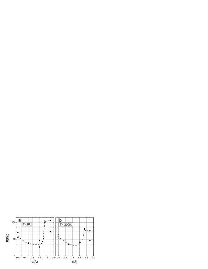
The tunnelling resistance of the studied Si doped MTJs measured at 2 K and 300 K, in the zero bias limit, is plotted in Fig. 2. The observed enhancement of the resistance when the temperature is lowered rules out the presence of pinholes even for the highest silicon thickness Rudiger et al. (2001); Jonsson-Akerman et al. (2000). There is an increase of the resistance for 1.5 Å, both at room and low temperatures, whereas at lower concentrations the resistance trend is to decrease. This fact indicates a change of the regime in the conductance, which will be further confirmed in the dependence of the conductance on the bias voltage and the TMR.
III.1 Dependence of the conductance on the voltage at low temperatures
While at room temperature conductance is a parabolic function of the bias, at low temperatures (below 100 K), the dependence of conductance on the bias changes substantially. On the one hand, all MTJs at low biases (V30 mV) present a peak in the resistance. Usually such a peak is called zero bias anomaly (ZBA). On the other hand, high bias conductance regimes (above 100 mV) show a strong variation with silicon thickness.
To show more clearly the qualitative change of conductance regime with Si doping we present the bias dependence of the normalized conductance
| (1) |
The dependence of ZBA vs. Si thickness, plotted in Fig. 4, shows that the resistance peak, being weakly dependent on for low Si thickness, strongly increases for the high doping region. The crossover region corresponds to the thickness of approximately =1.2 Å.
The experimental data presented above may be understood within the two-step model as follows. If the formation of silicon islands starts for a Si thickness =1.2 Å, then the enhanced resistance peak (ZBA) could be attributed to the appearance of a new energy scale in the electron transport through the barrier, related with the finite electron capacitance of the silicon islands, being practically absent for the small Si thickness range. This hypothesis is supported by the plot of the normalized bias voltage dependence of the conductance, Fig. 3. Clearly in the conductance of the junctions with higher Si doping levels there is a crossover at a certain voltage. At higher voltage the dependence of the conductance becomes less pronounced, whereas the junctions with low doping maintain the same behavior, as expected in a non-doped tunnel junction with electron transport due to direct tunneling.
The change of the conductance regime is also evident from comparison of the lower bias conductance for undoped MTJs and those with highest Si doping (corresponding to =1.8 Å). As can be seen in the (b) graph in Fig. 3, both curves show structure in G(V) at low bias close to V=30 mV. The similarity of these weak anomalies both for the undoped and doped MTJs indicate their common origin, most probably related with electron conduction mechanisms through the aluminium oxide barrier.


We have observed that generally, for all MTJs studied, the low bias conductance varies linearly with temperature at low temperatures (T<20 K). Within the Coulomb blockade model this could be attributed to a variation in the thermally activated population of electrons inside the islands Wolf (1989), which determines the slope of the conductance at zero bias. In brief, the conductance at zero bias and low temperatures could be expressed as
| (2) |
where is the charging energy needed to introduce an electron in the metallic layer. At 0 V the number of charged islands is given by the exponential term. Then, at low temperatures, the conductance is proportional to the number of charged particles in thermal equilibrium . Although the temperature dependence of conductivity of the different MTJs studied varies in nearly two orders of magnitude, the normalized (to 2 K) low temperature slope in the linear dependence of conductivity vs. temperature was found to be much weakly dependent on the silicon thickness, with an average value of K-1 but with a rather large dispersion (Fig. 5).

III.2 Tunneling magnetoresistance
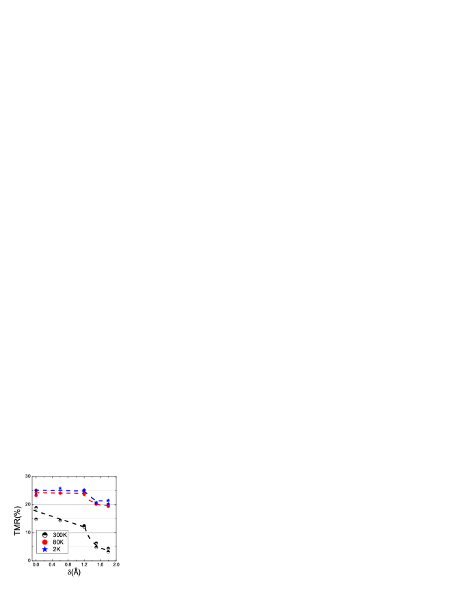
The dependence of the tunnelling magnetoresistance on Si thickness is shown in figure 6. This plot represents the zero bias tunnelling magnetoresistance, obtained by using the following definition of TMR
| (3) |
where and are the resistance in the antiparallel and the parallel states, respectively.
We have analyzed zero bias TMR vs. Si thickness for three different temperatures (300 K, 80 K, 2 K). The influence of the silicon doping on TMR is strongest at room temperature, suppressing TMR in nearly one order of magnitude for the highest Si thickness (1.8 Å). The low temperature TMR values, however, remain nearly unaffected by the silicon. The step-like reduction of TMR at low temperatures (of about 10 at 77 K and 2 K) was observed for a Si thickness of 1.2 Å. This apparent reduction of the tunnelling magnetoresistance may be directly linked to variation of the ZBA with Si content (shown in Fig. 4).
Indeed, for small Si thickness, only direct tunnelling is possible, due to Coulomb blockade. This weakly changes TMR at low temperatures for small bias, which does not activate possible spin mixing due to the spin flip processes introduced by the Si. The Coulomb blockade is suppressed for the doping range of 1.5 Å, as indicated by conductance vs. voltage measurements (Fig. 3), opening new conductance channels related to two-step tunnelling via the array of Si dots. The newly opened conductance channels create also a source of unpolarized current due to spin mixing and loose of spin memory of the electrons tunnelling through the array of Si dots. Suppression of Coulomb blockade just for the Si thickness bigger than 1.2Å could be due to activation of a segregation process of Si atoms to nanometer scale dots, acting as a real capacitance. This is contrary to the behaviour in low Si thickness junctions, where seems reasonable to suppose that Si could be more homogenously diluted inside the Al2O3 barrier in form of impurities and defects. In fact, two step tunnelling could, in principle, affect the conductance for both regimes discussed above. This is due to the unavoidable presence of defects inside the barrier, even without Si doping Guerrero et al. (2006), which mix the spin currents and are a source of an unpolarized current. Therefore, this implies the presence of a finite characteristic spin-flip time on the defects and on the silicon layer both for the low and the high Si thickness regimes Barnas and Fert (1999).
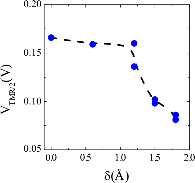
The analysis of bias dependence of TMR which follows further supports our hypothesis. In order to analyze the bias dependence of TMR as a function of Si thickness, we have found the voltage needed to suppress a TMR to its half (zero bias) value (i.e. to TMR(0 V)/2). This parameter, called is shown in Fig.7, plotted as a function of the silicon thickness. Evidently, there is a crossover from a nearly constant regime below =1.2 Å, to a strongly decreasing one as a function of , for Si thicknesses above one monolayer. The low Si doping regime with nearly constant proves the presence of two step tunnelling through localized states, with character and density of states nearly unchanged up to Si thickness of 1.2 Å.
When seems that the effective capacitance corresponding to localized states inside the barrier is reduced, increasing dramatically the number of states available inside the barrier for tunnelling. The new transport channels serve as a source of unpolarized current, which explains the much stronger voltage dependence of TMR for large Si doping.
IV Theoretical model
To account for the above discussed experimental features of electronic transport in tunnel junctions, we calculate now theoretically transport characteristics as a function of bias voltage using the model of rectangular tunneling barrier with a thin layer of impurities (Si atoms) which create a number of impurity levels inside the barrier. In the limit of low density of Si levels, the current is due to direct tunneling in each spin channel, and the current density can be calculated from the formula
| (4) |
where is the in-plane wavevector component of an electron incident on the barrier, is the transmission amplitude for an electron with wavevector and spin , while and are the spin-dependent energy band edges on the left and right sides of the junction, respectively, which depend on the applied voltage as and (here and are the corresponding band edges at zero voltage). Apart from this, the integration in Eq. (4) is over the electron energy , and is the Fermi-Dirac distribution function.
To calculate the tunneling probability for a nonzero voltage applied to the system we use a semiclassical approximation for the wavefunction inside the barrier with a slope of potential. This is justified in case when the variation of the barrier height is small at the electron wavelength , which restricts the bias voltage to , where is the barrier width.
IV.1 Impurity-mediated tunneling
As the density of impurities grows, an additional mechanism of tunneling through the impurity levels inside the barrier becomes more effective than the direct tunneling. In the frame of the Larkin-Matveev Larkin and Matveev (1987) model, the resonant tunneling through the structure is described by the transition probabilities . More specifically, is the probability of transition from the state described by the wavevector on the left side of the barrier to the state corresponding to the wavevector on the right side (from now on we drop the spin index referring to the tunneling in different spin channels), and is given by the formula
| (5) |
where and are the matrix elements for transitions between the states of the corresponding leads and of the -th impurity, whereas is the width of the impurity level associated with tunneling from the localized level through the barrier. The sum in Eq. (5) runs over all impurities. The factor is the imaginary unit.
An important point is that the matrix elements and include a phase factor depending on the location of the impurity inside the barrier,
| (6) |
| (7) |
where is the junction area, and are the in-plane and out-of-plane components of the -th impurity position, (and similarly for ), while is the inverse localization length of the impurity wavefunction. We assume that the impurities are randomly distributed in the plane, i.e. is a random variable, whereas is the same for all impurities.
Assuming that the energy level and the level width do not depend on the position , and averaging over in the plane, we obtain the following formula for the electric current:
| (8) |
After calculating the average , one finds that the current density in the resonance-impurity channel consists of two terms, and can be written as
| (9) |
The first term in Eq. (9) is linear in the 2D impurity density and describes the transitions through completely isolated single levels. Such transitions do not conserve the in-plane components of and . The second term in Eq.(9) is nonlinear in and describes the electron transitions through the impurity plane. For such transitions the corresponding in-plane components of electron wavevectors are conserved.
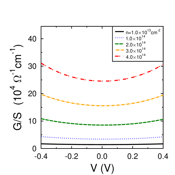
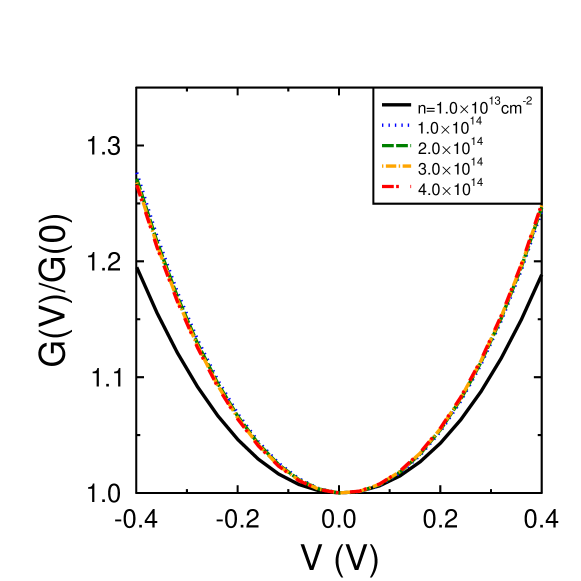
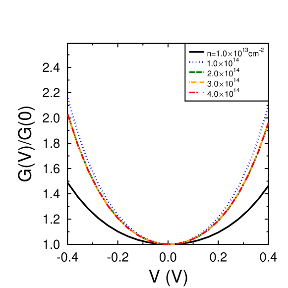
In our calculations we include all three channels. The total conductance per unit area, , is presented in Fig. 8 for parallel magnetic configuration and for indicated impurity concentrations. The width of the tunnel barrier is taken as nm, and the Si atoms are located within the plane of nm, measured from the center of the barrier. The energy structure corresponds to the majority and minority bands in Co, eV and eV, respectively. The height of the barrier is assumed to be eV. In turn, in Fig. 9 we show the reduced conductance, .
It should be noted that the conductance as well as the reduced conductance are slightly asymmetric with respect to bias reversal, see Fig. 8 and Fig. 9. This asymmetry is here associated with tunneling through single impurity levels which are located asymmetrically within the barrier. In our calculations we assumed that the impurities are located in the barrier close to the interface between the barrier and one of the electrodes – like in experiments discussed above. Such an asymmetry of impurity position with respect to the center of tunnel barrier leads to the asymmetry of the conductance .
IV.2 Role of Coulomb interaction
When the density of impurity levels grows, the conductance calculated within the model described above and including both direct and impurity-mediated tunneling increases monotonically (see Fig. 8). The experimental data (Fig. 2), however, reveal a rather sharp increase of the resistance to much higher values when the density crosses a critical value corresponding to nearly complete filling of one atomic layer with Si atoms. The results for TMR presented in Figs. 6 and 7 also show that the physics of tunneling is substantially different for the density of Si atoms corresponding to complete filling of the plane.
We assume that the physical reason of such transition is related to a dramatic increase of the role of Coulomb interaction in the conductance through the Si levels. This effect can be also described by the decrease of the number of active levels, which are able to transmit electrons through the barrier. Indeed, if some Si atoms form a small cluster, then the cluster of several atoms acts as a single level for transmission because the Coulomb interaction prevents two or more electrons to occupy the same cluster. Thus we can assume that Eq. (9) describes the conductance as a function of the density of effective levels, , corresponding to the number of impurity clusters. As the density of Si atoms approaches the critical value , the value of decreases rapidly. If and the density of Si atoms keeps growing then it corresponds to increasing thickness of the layer completely filled with the Si atoms. In such a case the Coulomb interaction is suppressed as there are no small clusters anymore, and the conductance can be described using a model of three-layer structure with well-defined properties of each of the layers. One can expect that the properties of the Si layer in such a structure are close to those of layered amorphous Si.
It should be emphasized that the direct tunneling is also suppressed in the vicinity of . This is related to the Coulomb repulsion of electrons transmitted through the barrier from the charged impurity clusters, so that the electrons can tunnel through the barrier only in those areas, which are free from the impurity clusters or islands. One can describe this by a local increase of the tunneling barrier in the areas filled with clusters. This effectively leads to an increase of the average tunneling barrier.

Using the above described ideas we have calculated the resistance as a function of , taking into account all three channels of conductivity as described above, but instead of the number of impurities we put in Eqs. (8),(9) an effective number of levels , which we assumed to change rapidly from at cm-2 to a constant value cm-2. We also corrected the contribution due to direct tunneling making it strongly dependent on in the vicinity of the transition point . More specifically, we reduced this contribution for by modeling the dependence of the tunnel barrier on : for we take independent of but for we assume that this value increases by eV, which corresponds to suppression of the direct tunneling due to the ’screening’ from the large impurity clusters within the Si layer. The results for the resistance as a function of are presented in Fig. 10. As one can note, the theoretical curve is qualitatively similar to the experimental one.
Further improvement of the model can be made by taking into account the dependence of the impurity density of states on energy in the vicinity of the Fermi level, . One can assume that the function has a minimum near in accordance with the shape of the density of states (DOS) in amorphous Si (see, for example, Refs. Lee and Chang (1994); Allan et al. (1998)). The DOS profile in the vicinity of the minimum at in amorphous a-Si can be approximately presented as a sum of the DOS tails related to the conduction and valence bands, , where eV-1atom-1, and meV. In the vicinity of the minimum at one can use the parabolic approximation
| (10) |
where .
V Discussion
Several attempts have been made previously trying to understand the possible role of Coulomb blockade in the tunnelling current and magnetoresistance for ferromagnetic leads contacting a quantum dot Barnas and Fert (1998); Barnaś et al. (2000). These works predict an oscillation in TMR(V) with a period given by the charging voltage. Experimentally, for tunnelling through an array of dots, the oscillatory behaviour has been reported only for the magnetic tunnelling junctions with a barrier doped with cobalt nanoparticles. Those junctions had rather small ferromagnetic electrodes area A=0.50.5 m2 with the conduction almost completely blocked at low bias Yakushiji et al. (2002), and TMR oscillating with the period predicted theoretically. Other experiments, which also studied spin dependent electron transport through arrays of dots doping the barrier of magnetic tunnel junctions, have reached conclusions in respect to conductance similar to those reported here, i.e observation of a non-oscillating increase of the conductivity with bias, when Coulomb blockade is suppressed by the applied voltage Ono et al. (1996); Schelp et al. (1997); Brückl et al. (1998); Shyu et al. (2003).
The above cited reports employed different devices in order to study spin dependent tunnelling through a medium controlled by Coulomb blockade, and two of them specifically Ref. Schelp et al. (1997) and Ref. Yakushiji et al. (2002) used qualitatively similar magnetic tunnel junction devices. In these papers a granular film, consisting of nanometer size cobalt particles (with radius close to 2.5 nm) was embedded in a matrix of aluminium oxide. This array of Co dots was deposited on top of the aluminium oxide barrier (2.7nm in the first case Schelp et al. (1997) and 1-2 nm in the second one Yakushiji et al. (2002))and was covered by the second aluminium oxide barrier. The top barrier was different in the studies mentioned above. While the first paper Schelp et al. (1997) used a 1.5 nm thick secondary barrier, the later work did not use any alumina barrier to cover the Co nanoparticles, which probably produced an uncontrolled secondary barrier. Another difference is related to the junctions area. In the first study a rather big (4.510-2 mm2) area MTJ was used, while the second work studied Coulomb blockade controlled spin dependent tunnelling in MTJ’s with much smaller area junction. All different studies of the spin dependent transport in MTJ’s with nanoparticle doped barrier, with the exception of Yakushiji et al., Yakushiji et al. (2002), reported a staircase dependence of the IVs presumably due to single electron charging effects, and did not show any conductance oscillation.
Although our samples have a silicon layer inside the barrier, instead of a magnetic layer introduced in the previous reports, the observed behaviour of the conductance vs. voltage is in general similar to the data reported for spin tunnelling through arrays of magnetic nanoparticles Schelp et al. (1997), with exception of the dependence of TMR on bias voltage which is smoother (V0.5 V, Schelp et al. (1997)) than in our samples.
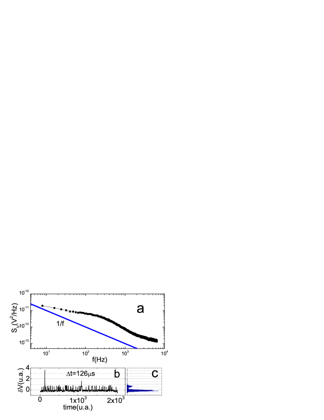
A further confirmation of the role of the Coulomb blockade in our samples could be observed in the noise at low frequency in the studied samples. Whereas for low Si doping ( 1.2 Å), the power spectrum at low temperatures is ”white” (i.e. nearly frequency independent) and corresponds well to the shot noise expected for direct tunnelling in a tunnel junction (or for two-step tunnelling through strongly asymmetric barriers), for 1.5 Åa random telegraph noise (RTN), Fig. 12, contribution becomes evident for bias voltages above a critical value. The appearance of RTN for 1.2 Åmight be understood as a consequence of the suppression of Coulomb blockade.
RTN has been previously reported for nonmagnetic tunnel junctions and some other devices such as field effect transistors or quantum dots connected to metallic leads Peters et al. (1999). As to the tunnel junctions, RTN has been usually attributed to resistance fluctuations due to a single or few fluctuators Kogan (1996). The RTN was usually found for rather small area (below 1m2) junctions and low temperatures, because in this case the tunnel resistance is controlled by a few fluctuating defects, providing two-state fluctuations of the resistance. In the case of rather large tunnel junctions, as in the present study, the observation of RTN could not be described by the above models, involving direct influence of single or few defects fluctuations on the resistance. A non-uniform current distribution, induced by pin-holes, which are a source of ”hot spots” just before the MTJs are broken down by the intensity of current, would neither explain the observed voltage dependence of the RTN. Indeed, our experimental data, particularly the current-voltage characteristics and the temperature dependence of the conductance show absence of pinholes and the above mentioned ”hot spots”.
As discussed above, for thick enough silicon layers 1.2 Å the effective capacitance of the Si dots becomes small enough to break down the Coulomb blockade above a certain bias voltage. This increases the electron population of the island due to the two steps tunnelling events and enhances the tunnelling conductance.
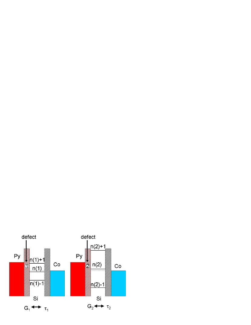
It is evident that in the system under study the capacitance of the Si dots and, correspondingly, the Si dots population, should be distributed over the MTJ area, providing a possible variation of the local tunnelling current as a function of the spatial coordinate. In addition, the two-level systems situated close to the Si dots seem to introduce also time dependent fluctuations or RTN in the tunnelling current through these dots. The unavoidable dependence of the tunnelling current on the coordinate may enhance the effective contribution to the overall conductance from only a few fluctuators, resulting in a noise contribution additional to 1/ due to effective ”amplification” of some conductance fluctuations responsible for RTN from these few defects. This is represented schematically in the Fig. 13: the change in the charge in the defect yields two states with different tunneling rates (), hence different conductance. The origin of the different times lies in the different levels inside the dots, which are determined by the capacitance, thus by the local environment. Of course, in our tunnel junction there are many defects, but at low temperatures there are only several of them active because the trapping-detrapping process uses to be thermally activated.
VI Conclusions
To conclude, we have carried out an extensive study of electron transport in CoAl2O3Py magnetic tunnel junctions asymmetrically doped with Si. Our experimental data suggest that the observed behaviours of conductance vs Si doping are closely related, clearly indicating a suppression of the Coulomb blockade regime for Si layer thicknesses above about one monolayer. Although no staircase behavior of the conductance was observed for the regime of suppressed Coulomb blockade, as in some other systems Yakushiji et al. (2002), the observed behavior of tunnelling conductance is rather similar to the one reported long time ago by Giaever Zeller and Giaever (1969), which was successfully explained as due to the presence of a large amount of particles inside the barrier. For a fixed bias voltage applied in equilibrium, these particles might have very different electron population, even though their capacitances are characterized by rather narrow size distributions, giving rise to some distribution of the maximum threshold voltage suppressing Coulomb blockade Vch. This leads to the observed zero bias anomaly in our samples. On the other hand, the variation of the electron population in each particle may explain the suppression of the predicted Barnas and Fert (1998) Coulomb oscillations, which could be present only for a constant equilibrium electron population in Si particles across the junction area. One of the ways to reach a more uniform electron population in the Si particles could be the reduction of the area of the junctions as in Ref. Yakushiji et al. (2002), implying tunnelling through a smaller array of nanoparticles with a size distribution narrower than in the present case.
Acknowledgements.
This work was supported by funds from the Spanish Comunidad de Madrid (Grant No. P2009/MAT-1726) and Spanish MICINN (Grants No. MAT2006-07196, No. MAT2009- 10139, Consolider Grant No. CSD2007-00010). As a part of the European Science Foundation EUROCORES Programme Grant No. 05-FONE-FP-010-SPINTRA, work was supported by funds from the Spanish MEC (MAT2006-28183-E), Polish Ministry of Science and Higher Education as a research project in years 2006 2009, and the EC Sixth Framework Programme, under Contract No. ERAS-CT-2003-980409. The work was also supported by ESF-AQDJJ programme, FCT Grant PTDC/FIS/70843/2006 in Portugal, and by the Polish Ministry of Science and Higher Education as a research project in years 2007 2010 (V.K.D.). Work in MIT is supported by NSF Grant No. DMR-0504158 and ONR Grant No. N00014-06-1-0235.References
- Miyazaki and Tezuka (1995) T. Miyazaki and N. Tezuka, Journal of magnetism and magnetic materials 139, L231 (1995).
- Moodera et al. (1995) J. Moodera, L. Kinder, R. Wong, and R. Meservey, Physical Review Letters 74, 3273 (1995).
- LeClair et al. (2002) P. LeClair, J. K. Ha, H. J. M. Swagten, J. T. Kohlhepp, C. H. van de Vin, and W. J. M. de Jonge, Applied Physics Letters 80, 625 (2002).
- Yuasa et al. (2006) S. Yuasa, A. Fukushima, H. Kubota, Y. Suzuki, and K. Ando, Applied Physics Letters 89, 042505 (2006).
- Schelp et al. (1997) L. F. Schelp, A. Fert, F. Fettar, P. Holody, S. F. Lee, J. L. Maurice, F. Petroff, and A. Vaurès, Phys. Rev. B 56, R5747 (1997).
- Shyu et al. (2003) J. H. Shyu, Y. D. Yao, C. D. Chen, and S. F. Lee, Journal of Applied Physics 93, 8421 (2003).
- Takahashi et al. (1999) S. Takahashi, H. Imamura, and S. Maekawa, Physical Review Letters 82, 3911 (1999).
- Maekawa (2006) S. Maekawa, Concepts in Spin Electronics (Oxford University Press, New York, 2006).
- Yakushiji et al. (2002) K. Yakushiji, S. Mitani, K. Takanashi, and H. Fujimori, Journal of Physics D-Applied Physics 35, 2422 (2002).
- Ono et al. (1996) K. Ono, H. Shimada, S. ichi Kobayashi, and Y. Ootuka, Journal of the Physical Society of Japan 65, 3449 (1996).
- Bernand-Mantel et al. (2006) A. Bernand-Mantel, P. Seneor, N. Lidgi, M. Mu oz, V. Cros, S. Fusil, K. Bouzehouane, C. Deranlot, A. Vaures, F. Petroff, and A. Fert, Applied Physics Letters 89, 062502 (2006).
- Deshmukh and Ralph (2002) M. M. Deshmukh and D. C. Ralph, Phys. Rev. Lett. 89, 266803 (2002).
- Jensen et al. (2005) A. Jensen, J. R. Hauptmann, J. Nygrd, and P. E. Lindelof, Physical Review B 72, 035419 (2005).
- Pasupathy et al. (2004) A. N. Pasupathy, R. C. Bialczak, J. Martinek, J. E. Grose, L. A. K. Donev, P. L. McEuen, and D. C. Ralph, Science 306, 86 (2004).
- Slonczewski (1989) J. Slonczewski, Physical Review B 39, 6995 (1989).
- Bratkovsky (1997) A. M. Bratkovsky, Phys. Rev. B 56, 2344 (1997).
- Zhang et al. (1997) S. Zhang, P. M. Levy, A. C. Marley, and S. S. P. Parkin, Physical Review Letters 79, 3744 (1997).
- Moodera et al. (1998) J. S. Moodera, J. Nowak, and R. J. M. van de Veerdonk, Phys. Rev. Lett. 80, 2941 (1998).
- Ding et al. (2003) H. F. Ding, W. Wulfhekel, J. Henk, P. Bruno, and J. Kirschner, Physical Review Letters 90, 116603 (2003).
- Zeller and Giaever (1969) H. R. Zeller and I. Giaever, Phys. Rev. 181, 789 (1969).
- Glazman and Matveev (1988) L. Glazman and K. Matveev, JEPT Letters 48, 445 (1988).
- Larkin and Matveev (1987) A. I. Larkin and K. A. Matveev, Zh. Eksp. Teor. Fiz. 93, 1030 (1987).
- Jansen and Moodera (2000) R. Jansen and J. S. Moodera, Phys. Rev. B 61, 9047 (2000).
- Moodera et al. (1997) J. S. Moodera, E. F. Gallagher, K. Robinson, and J. Nowak, Applied Physics Letters 70, 3050 (1997).
- Jansen et al. (2000) R. Jansen, B. Davis, C. T. Tanaka, and J. S. Moodera, Surface Science 463, 109 (2000).
- Guerrero et al. (2005) R. Guerrero, F. G. Aliev, R. Villar, J. Hauch, M. Fraune, G. Güntherodt, K. Rott, H. Brückl, and G. Reiss, Applied Physics Letters 87, 042501 (2005).
- Brinkman et al. (1970) W. Brinkman, R. Dynes, and J. Rowell, Journal of Applied Physics 41, 1915 (1970).
- Rudiger et al. (2001) U. Rudiger, R. Calarco, U. May, K. Samm, J. Hauch, H. Kittur, M. Sperlich, and G. Guntherodt, Journal of Applied Physics 89, 7573 (2001).
- Jonsson-Akerman et al. (2000) B. J. Jonsson-Akerman, R. Escudero, C. Leighton, S. Kim, I. K. Schuller, and D. A. Rabson, Applied Physics Letters 77, 1870 (2000).
- Wolf (1989) E. Wolf, Principles of Electron Tunneling Spectroscopy (Oxford science publications, New York, 1989).
- Guerrero et al. (2006) R. Guerrero, F. G. Aliev, Y. Tserkovnyak, T. S. Santos, and J. S. Moodera, Physical Review Letters 97, 266602 (2006).
- Barnas and Fert (1999) J. Barnas and A. Fert, Journal of Magnetism and Magnetic Materials 192, L391 (1999).
- Allan et al. (1998) G. Allan, C. Delerue, and M. Lannoo, Physical Review B 57, 6933 (1998).
- Lee and Chang (1994) I.-H. Lee and K. Chang, Physical Review B 50, 18083 (1994).
- Barnas and Fert (1998) J. Barnas and A. Fert, Phys. Rev. Lett. 80, 1058 (1998).
- Barnaś et al. (2000) J. Barnaś, J. Martinek, G. Michałek, B. R. Bułka, and A. Fert, Phys. Rev. B 62 (2000).
- Brückl et al. (1998) H. Brückl, G. Reiss, H. Vinzelberg, M. Bertram, I. Mönch, and J. Schumann, Phys. Rev. B 58, R8893 (1998).
- Peters et al. (1999) M. Peters, J. Dijkhuis, and L. Molenkamp, Journal of Applied Physics 86, 1523 (1999).
- Kogan (1996) S. Kogan, Electronic Noise and Fluctuations in solids (Cambridge University Press, Cambridge, 1996).