Optical absorption spectrum in disordered semiconductor multilayers
Abstract
The effects of chemical disorder on the electronic and optical properties of semiconductor alloy multilayers are studied based on the tight-binding theory and single-site coherent potential approximation. Due to the quantum confinement of the system, the electronic spectrum breaks into a set of subbands and the electronic density of states and hence the optical absorption spectrum become layer-dependent. We find that, the values of absorption depend on the alloy concentration, the strength of disorder, and the layer number. The absorption spectrum in all layers is broadened because of the influence of disorder and in the case of strong disorder regime, two optical absorption bands appear. In the process of absorption, most of the photon energy is absorbed by the interior layers of the system. The results may be useful for the development of optoelectronic nanodevices.
I Introduction
Low-dimensional quantum structures, such as quantum wells and superlattices, wires and dots have attracted great interest in the last few years, due to their possible application in nanodevices Harrison . Among these structures, multilayers and superlattices, with thickness of few nanometers, are of considerable experimental and theoretical interest because of their specific electronic and optical properties and many promising areas of applications. For example, multilayer semiconductors are very useful for laser diodes, leading to low threshold current, high power, and weak temperature dependence devices Razeghi .
It has been demonstrated that, by using semiconductor nanostructures instead of bulk structures, the threshold current may be reduced by more than ten times due to the abrupt energy dependence of the density of states in low-dimensional structures which can enhance the light amplification mechanisms and thus allows lasing to occur at lower currents Asada . Furthermore, the optical absorption in semiconductors which is governed by the electronic density of states, is strongly affected by the impurities Fuchs ; Shinozuka1 ; Shinozuka2 . For instance, using a semiconducting alloy A1-xBx, composed of two semiconductors A and B with different band gap energies, one can tune the operation of an optical device at desired wavelength.
There are many different theoretical approaches that can be used for studying the electronic properties of disordered semiconductors (see for instance Gonis ). Among them, the coherent potential approximation (CPA) Soven ; Velick ; Gonis is one of the most widely used methods to study chemically disordered systems. In this approximation the multiple scattering on a single site is taken into consideration and this approach is fairly good for any values of bandwidth and scattering potential.
According to the work of Onodera and Toyozawa Onodera ; Toyozawa , the optical absorption spectra of substitutional binary solid solutions can be classified into persistence and amalgamation types in a unified theory. In the persistence type, two exciton peaks corresponding to the two constituent substances are observed, as seen in alkali halides with mixed halides such as KCl1-xBrx. In the amalgamation type, however, only one exciton state appears, which can be seen in alkali halides with mixed alkalis such as KxRb1-xCl. These two typical cases can be distinguished by a parameter which is the ratio of the difference of the atomic energies in the two constituent substances to the energy-band width. In the persistence type, this difference is large compared to the bandwidth and the electronic spectrum is split into two bands, while, when this ratio is small, the impurity band is united with the host band and in this case, which corresponds to the amalgamation type, a single band appears. We should note that the transition from the amalgamation type to the persistence type also depends on the value of impurity concentration Onodera .
Based on the Onodera-Toyozawa theory and the CPA, optical properties of various disorder systems have been investigated Yoshikawa ; Shinozuka1 ; Shinozuka2 ; Bakalis ; Takahashi . Recently, Shinozuka et al. Shinozuka1 ; Shinozuka2 studied the effect of chemical disorder on the electronic and optical properties of bulk, quantum well and wire systems within the CPA. Because of the absence of periodicity in the confinement directions in the quantum wells and wires, the electronic and optical properties of these systems become site-dependent. In their calculations, however, such a dependence has not been included. This site-dependence may be important in operation of nanoscale devices and will be included in our calculations.
The aim of this work is to extend the CPA for the doped semiconductor multilayers to investigate the influence of substitutional disorder on the local density of states (LDOS) and optical absorbtion spectrum in each layer of the system and in both the persistence and amalgamation types. The paper is organized as follows: in Sec. II, by applying the single-site approximation to the layered structures in the presence of chemical disorder, we present our theory and derive equations for the LDOS and optical absorption. The numerical results and discussion for the behavior of desired quantities in terms of the alloy concentration and the scattering-strength parameter are given in Sec. III. The concluding remarks are given in section IV.
II Model and formalism
We consider a multilayer structure where the layers are stacked along the -direction and labeled by integer number . The number of layers in this direction is , hence . The lattice structure of the system is assumed to be a simple cubic with lattice spacing and the (001) orientation of the layers is taken to be normal to these layers. The multilayer is a semiconducting alloy of the form , where atom (such as Si) and atom (such as Ge) occupy randomly the lattice sites with concentration . We use the single-band tight-binding approximation with nearest-neighbor hopping and the on-site delta function-like potential. The Hamiltonian for a single electron (or a Frenkel exciton) in this system is given by
| (1) |
where denotes the positional vector in the plane and the on-site potential is assumed to be and with probabilities and when the lattice site () is occupied by the and atoms, respectively. The arrangement of these atoms is completely random. The hopping integral is equal to for the nearest neighbor sites and zero otherwise. We assume that the hopping integral only depends on the relative position of the lattice sites, that is, only the diagonal disorder is considered. The introduced randomness is treated by the CPA Soven ; Gonis . In this approximation, one seeks to replace a disordered alloy with an effective periodic medium. This CPA medium is characterized by a local (i.e., momentum-independent), energy-dependent self-energy, , called the coherent potential. In some disordered low dimensional systems such as the quantum wires Nikolic ; Saffar and the multilayers Okiji ; Hasegawa , the self-energy depends on the position of atomic sites, due to the absence of translational symmetry in some directions. Therefore, in this study the self-energy depends on the layer number, i.e., because of the quantum confinement along the -direction. Accordingly, the multilayer Hamiltonian is replaced by an effective medium Hamiltonian defined by
| (2) |
The physical properties of the real system can be obtained from the configurationally averaged Green’s function which is replaced in the CPA with an effective medium Green’s function defined by the following Dyson equation Saffar
| (3) | |||||
where is the clean system Green’s function and its matrix element is given by
| (4) |
here, is the mixed Bloch-Wannier representation of and is expressed as
| (5) |
and
| (6) |
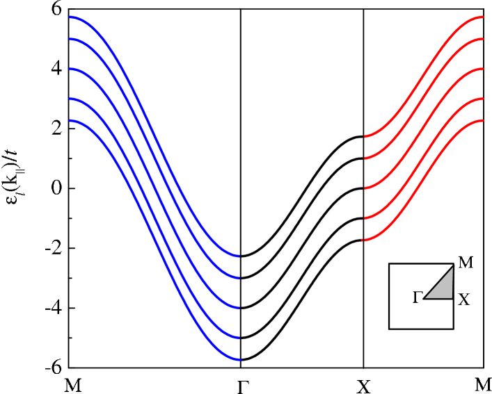
is the clean system band structure. In Eq. (4), is a wave vector parallel to the layer and the summation is over all the wave vectors in the first Brillouin zone (1BZ) of the two-dimensional lattice Gonis , is the mode of the subband, is the number of lattice sites in each layer, and is a positive infinitesimal.
Now, to determine the coherent potential in each layer (say ), we consider an arbitrary chosen site in the effective medium (layer) describe by . Then, we apply the condition that the average scattering of a carrier by the chosen site in the medium is zero. This condition for any site in the th layer is given by
| (7) |
where, is the single-site -matrix which represents the multiple scattering of carriers by and atoms in the effective medium, denotes average over the disorder in the system, and is the diagonal matrix element of the Green’s function of the th effective layer and for can be written as
| (8) |
We should note that, the effective Green’s function, , depends on and the two dimensional wave vector via .
From Eq. (7) one can derive an equation for the self-energy of th layer. Then, using such an equation and also Eq. (3), which gives a system of linear equations, one can obtain self-consistently the self-energy and the Green’s function in each layer. Then, the LDOS in the th layer is calculated by
| (9) |
In order to calculate the optical absorption spectrum, we assume that both the and atoms have equal transition dipole moments Onodera ; Toyozawa . Accordingly, when the th subband is optically excited the layer-dependent optical absorption is given by the component of the LDOS. The reason is that (i.e., point in the inset of Fig. 1) is the bottom of the conduction band at each layer. We should note that, in the case of bulk materials, (in three dimensions) is the minimum point in the exciton band. In this study gives the minimum energy for each subband. Therefore, the optical absorption of the th layer, due to the creation of an exciton in the system, can be expressed as
| (10) |
If it is assumed that, the self-energy does not depend on the layer number (i.e., the assumption of translational invariant along the -direction), then a simple expression for Eq. (10) is obtained, as it was assumed in Refs. Shinozuka1 ; Shinozuka2 . In the present work, the behavior of this function in each layer of the system which depends on the number of layers, alloy concentration and the strength of scattering processes via the self-energy will be studied in Sec. III.
III Results and discussion
To study the electronic and optical properties of the system, we perform our numerical results for and characterize the scattering-strength parameter by , where is the half-bandwidth of either constituent. We also emphasize that, the calculation of is not restricted to the lowest subband, because the results showed that component in other subbands is finite and hence, all the subband contributions must be included.
In order to see the effect of quantum confinement on the clean system, is shown in Fig. 1 along the high symmetry directions in the 1BZ. We observe five energy subbands due to the five atomic layers. Each of the subbands crosses the energy axis at the symmetry points with vanishing slope. In other words, there are states with zero group velocity which are responsible for the singularities in the LDOS of each layer and will be shown below in the case of and . Since the behavior of electronic states and the modification of energy band due to the influence of chemical disorder play a significant role in determining the optical properties of the disordered system, the LDOS should be analyzed in detail.
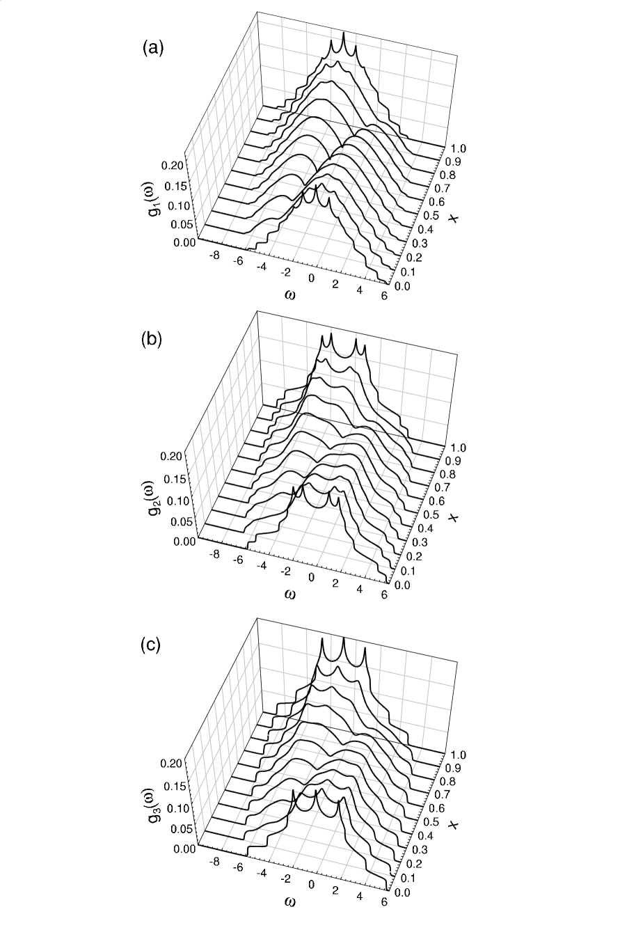
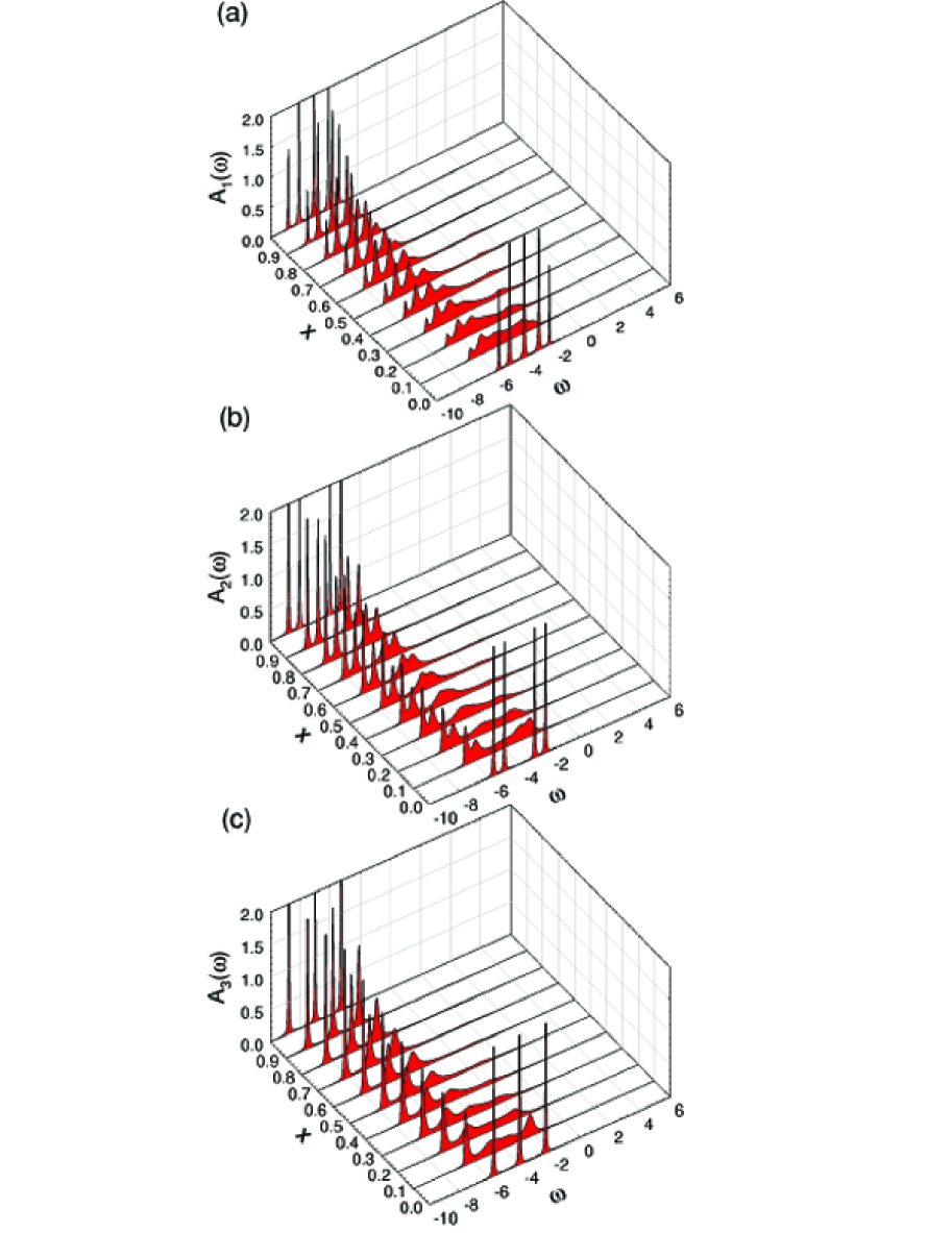
In Figs. 2 and 3 we plot the layer-dependence of LDOS and the optical absorption spectrum for which corresponds to . Because of the symmetry of the system in the -direction, the electronic states for the layers =1 and , and also for and are similar to each other. For this reason, we have investigated our desired quantities in the layers =1, 2, and 3. The figures show how the value of alloy concentration influences the and . In the case of and , the LDOS of all layers shows a steplike behavior for the states around the bottom and the top of the band, while, sharp features are observed for energies around the center of band. Both the steplike and sharp features (van-Hove singularities) in the LDOS, which correspond to the symmetry points of the 1BZ, comes from the two-dimensional nature of the multilayer. The position of sharp peaks in the electronic density of states is different in various layers due to the quantum confinement along the confined direction. With increasing the electronic spectra are shifted to the low-energy side and the steplike behavior and sharp peaks gradually disappeared. In the case of maximum disorder, i.e., at the LDOS is completely symmetric with respect to the center of band. The steplike and sharp features in the localized states are reproduced for . Also, it is clear that, a cusp may appear in the LDOS, depending on the value of alloy concentration. This effect, which is related to the value of , confirms that such electronic spectra belong to the amalgamation type.
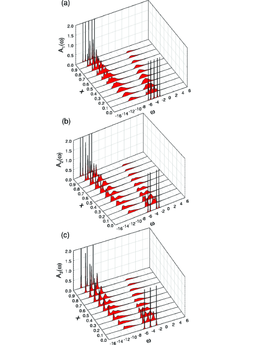
In a clean system, i.e., in the case of or , shows sharp peaks at the edges of the subbands. However, in a system with substitutional disorder, the absorption peaks are broadened and their heights decrease. Based on the behavior of electronic states, with increasing , as shown in Fig. 3, the optical absorption spectrum shifts to the low-energy side, due to its dependence on the bottom energy of the subbands. The maximum value of corresponds to the cases of and , because the van Hove singularities for these values of are significantly large. Thus, we can conclude that, in doped semiconductor multilayers, impurities with lower (higher) site energy in comparison with the energy of host atoms and with finite concentration , decrease the strength of optical absorption, i.e., the height of peaks in , and incident photons with low (high) energy are needed.
Another interesting feature is that optical absorption of the surface layers, i.e., layers and , is smaller than that of the interior layers, due to the influence of surface states [compare the maximum value of with that of and at the lowest energies in Fig. 3]. This indicates that in multilayer systems, the value of optical absorption in each layer depends on the layer number, and the interior layers play a major role in such a process. This feature, which has not been predicted in the previous studies Shinozuka1 ; Shinozuka2 , is important in operation of semiconductor optoelectronic nanodevices.
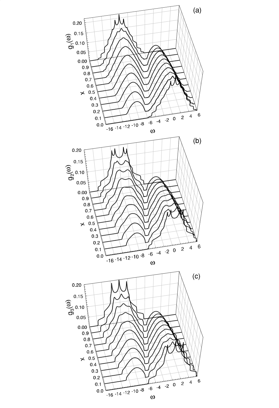
To investigate the another aspect of the electronic and optical properties of the system, we have shown in Figs. 4 and 5, and for which corresponds to . We can clearly see that a gap appears in the LDOS for each value of and the electronic spectra split into two bands corresponding to the two constituent crystals; the lower- (higher-) energy band in this figure corresponds to the () atoms. Accordingly, these electronic spectra belong to the persistence type. This gap opening is a consequence of scattering process of carriers by random distribution of the elements in the alloy, and its magnitude depends on the strength of disorder. Our analysis of the behavior of LDOS is similar to that of Fig. 2.
Fig. 5 clearly indicates that in the case of strong disorder regime, consists of two bands and the spectrum stretches toward the higher-energy side. With increasing , the optical absorption spectrum of the -type band decreases and shifts to the high-energy side, while the spectrum of the -type band increases and shifts to the low-energy side. Here, we should mention that, under certain conditions, the width of optical absorption spectrum in disordered quantum wires can be considerably stronger than that of the present system Fuchs . An interesting point in Fig. 5 is that, in spite of the symmetry of for with respect to the center of electronic spectrum, the optical spectrum is not symmetric and the lower band shows a higher value of absorption which is due to the fact that only the component contributes to this process.
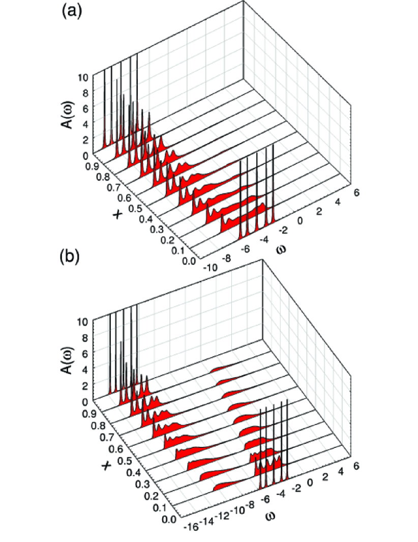
It is important to mention that the optical absorption spectrum from each layer is not a measurable quantity in experiment and only the bulk (total) optical absorption spectrum, , is possible. In order to obtain this quantity we should sum over the optical absorption of all layers, i.e., . The total optical absorption are shown in Fig. 6(a) and 6(b) for and , respectively. From the figures we see that, in the case of , the absorption spectrum has sharp peaks at the bottom of the optical band for all values of , and shows that the value of total optical absorption at the band minimum of the amalgamation type (Fig. 6(a)) is higher than that of the persistence type (Fig. 6(b)). The numerical results also confirm that, as in the bulk materials, the transition from the amalgamation type to the persistence type in multilayers depends on two parameters and Onodera ; Toyozawa .
IV Conclusion
Using the single-band tight-binding theory and the single-site CPA, we have studied the influence of substitutional disorder on the electronic and optical properties of disordered semiconductor multilayers. The results of this theory which is able to predict either the persistent or amalgamated bands, indicate that the optical absorption is governed by the electronic density of states, which is stronger near the bottom of the band. The values of absorption depend on the layer number, the concentration of chemical disorder, and the scattering-strength parameter. In addition, we found that the interior layers in comparison with the surface layer, have significant contribution in the optical absorption of the system.
The obtained results clearly indicate that, studying the dependence of quantum size effects on the optical properties of doped semiconductors is important for better understanding the process of optical absorption in layered structures, and will be helpful for designing optoelectronic nanodevices.
References
- (1) P. Harrison, Quantum Wells, Wires and Dots, Theoretical and Computational Physics (Wiley, New York, 2000).
- (2) M. Razeghi, Fundamental of Solid State Engineering, 2nd ed. (Springer, New York, 2006).
- (3) M. Asada, Y. Miyamoto, and Y. Suematsu, IEEE J. Quantum Electron. 22, 1915 (1986).
- (4) C. Fuchs and R.V Baltz, Phys. Rev. B 63, 085318 (2001).
- (5) Y. Shinozuka, H. Kida, and M. Fujibayashi, Phys. Stat. Sol. (b) 229, 553 (2002).
- (6) Y. Shinozuka, Jpn. J. Appl. Phys. 45, 8733 (2006).
- (7) A. Gonis, Green Functions for Ordered and Disorderd Systems (North-Holland, Amsterdam) Studies in Mathematical Physics, Vol. 4, (1992).
- (8) P. Soven, Phys. Rev. 156, 809 (1967).
- (9) B. Velický, S. Kirkpatrick, and H. Ehrenreich, Phys. Rev. 175, 747 (1968).
- (10) Y. Onodera and Y. Toyozawa, J. Phys. Soc. Jpn. 24, 341 (1968).
- (11) Y. Toyozawa, Optical Processes in Solids (Cambridge University Press, New York, 2003).
- (12) S. Yoshikawa and M. Aihara, J. Phys. Soc. Jpn. 76, 044712 (2007).
- (13) L.D. Bakalis, I. Rubtsov, and J. Knoester, J. Chem. Phys. 117, 5393 (2002).
- (14) M. Takahashi, Phys. Rev. B 70, 035207 (2004).
- (15) K. Nikolić and A. MacKinnon, Phys. Rev. B 47, 6555 (1993).
- (16) A. Saffarzadeh, Phys. Rev. B 76, 214201 (2007).
- (17) A. Okiji, H. Nakanishi, K. Sakata, and H. Kasai, Jpn. J. Appl. Phys. 31, L706 (1992).
- (18) H. Hasegawa, Phys. Rev. B 47, 15073 (1993).