Analytical study of non-linear transport across a semiconductor-metal junction
Abstract
In this paper we study analytically a one-dimensional model for a semiconductor-metal junction. We study the formation of Tamm states and how they evolve when the semi-infinite semiconductor and metal are coupled together. The non-linear current, as a function of the bias voltage, is studied using the non-equilibrium Green’s function method and the density matrix of the interface is given. The electronic occupation of the sites defining the interface has strong non-linearities as function of the bias voltage due to strong resonances present in the Green’s functions of the junction sites. The surface Green’s function is computed analytically by solving a quadratic matrix equation, which does not require adding a small imaginary constant to the energy. The wave function for the surface states is given.
Keywords:
Non linear transport, Keldysh, Surface states, Resonancespacs:
72.10.Fk, 73.20.-r, 73.21.Hb, 73.21.Hb1 Introduction
The electronic properties of surfaces and interfaces has many fascinating features, associated with the formation of surface states, modification of the band structure and corresponding density of states, and electronic transport Ibach . Strongly localized surface states are known since a long time to be present at the interface of semiconductors and metals Tamm and have been shown to influence the conductance of scanning tunneling microscopy (a quasi-one-dimensional process) Kobayashi . Also these states have recently been found in one-dimensional metamagnetic materials Kivshar . Therefore the characterization of these states is an important aspect of the physics of surfaces of materials and interfaces between two different solids.
In the fields of one-dimensional physics, specially those related to device applications, the transport properties are of crucial importante, and therefore it is important to study the effect that surfaces and interfaces have on these properties. Of particular interest to us is the non-linear transport through a semiconductor-metal interface. The non-linear transport requires the use of non-equilibrium methods, which were first introduced in this context by Caroli et al. Caroli . Following these early developments, the calculation of the current through a two-band system, connected to one-dimensional metals, including the effect of disorder on the semiconductor was soon performed Glick , and latter revisited by other authors Bishop . As old as these investigations may be, transport across one-dimensional metal-semiconductor-metal systems is still an active research topic Mathur , specially in the field of quasi one-dimensional organic conductors.
Except for very simple models, such as transport across an impurity Sautet88 ; Mizes91 ; Khomyakov05 ; Sols , the transport calculations using the non-equilibrium Green’s functions method are all numerical. This is so due to the fact that both the surface Green’s function of the contacts and the Green’s functions of the system (often called device) are obtained by the inversion of very large matrices, a process that in general has no analytical solution. There is even the wide-spread idea that the only surface Green’s function that can be computed analytically is that of a semi-infinite one-dimensional chain Sankey (the surface Green’s functions of a cubic lattice reduce to the solution of a onedimensional problem with analytical solution Ferry ).
Usually, the surface Green’s function of a given lead is computed using a recursive method developed long ago Rubio . The convergence of this method is constrainted by the value of a small imaginary positive number added to the energy of the Green’s function. There is however an alternative method to compute the surface Green’s function that does not depend on the value of that small imaginary part; it even works with the small imaginary part equal to zero, a limit that is implicit in the definition of the Green’s function Dy ; Dy2 . As we show bellow, this method can be used to obtain analytical expressions for the surface Green’s function of a system with two atoms per unit cell, by solving a quadratic matrix equation.
It is our purpose, in this paper, to study analytically, within a simple toy model, the formation of Tamm states at the interface of a semiconductor-metal junction and its non-linear transport, as a function of the bias voltage across such interface. We certainly recognize our study to be that of a toy model problem, but the fact that all quantities can be computed analytically makes our results relevant for the study of more sophisticated models where no analytical solution exists. We will compute all the needed Green’s function analytically, which in turn give analytical expressions for the tunneling probability and for the system density matrix. To our best knowledge this study has not been done before.
The paper is organized as follows, in Sec. 2 we formulate the problem in terms of an infinite dimensional block tridiagonal matrix and explain how to derive the needed Green’s function as well as the method of solution for the surface Green’s functions. In Sec. 3 we study the existence of surface states in the semiconductor and metal surfaces and how these states evolve to sharp resonances when the semiconductor and the metal are coupled. In Sec. 4 we compute the charge current through the interface for arbitrarily large bias voltage and the local electron occupation at the sites of the interface. Finally, in Sec. 5 we give our conclusions.
2 Hamiltonian toy model and formalism
In order to give a analytical description of the properties of a semiconductor-metal junction we consider here a one-dimensional model. In Fig. 1 we depict the model used. The unit cells have two atoms. In the case of the semiconductor the atoms are different ( and in Fig. 1); in the metal all the atoms are equal ( in Fig. 1). The doubling of the unit cell in the metal is only a matter of convenience, since it allow us to write the Hamiltonian as a tridiagonal block matrix (see below). The junction takes place in the unit cell . The terminal atoms of the semiconductor and the metal are represented by the letters and , respectively. In the semiconductor the hopping within a unit cell is and between unit cells is . In the metal the hopping is . The local energies in the semiconductor are and for atoms and , respectively, and for the metal atoms the local energy is represented by . In general we expect that the atoms at the surface of a metal, say, have different local energies and be connected to the bulk atoms by different hopping parameters. This fact introduces the parameters , , , . The hopping across the interface is . The reader may note that the model has a somewhat large number of parameters. This is necessary, since at the interface of both the metal and the semiconductor both the hopping and the on-site energies are modified relatively to their bulk values. Naturally, the number of parameters can be greatly reduced if we do not take into consideration the effect of the surface on the model parameters. Although our study is aimed to a general description of the effects of surfaces on the non-linear transport across an interface, its application to a real system is a possibility; this would require us to use the values of the parameters appropriate to the system under study. We note, however, that all energies are given in units of , and therefore the parameter values used in the simulations can apply to a general system.

If we denote the semiconductor Hamiltonian by , the metal Hamiltonian by , and the junction Hamiltonian by (defined by unit cell ), the full Hamiltonian of the problem, written in the local atomic basis, reads
| (1) |
where the matrices and are the coupling between the semiconductor and the junction and the metal and junction, respectively. If we write and explicitly, the Hamiltonian (1) acquires a block tridiagonal form and reads
| (2) |
where the several matrices are given by
| (3) |
| (4) |
| (5) |
and
| (6) |
Since we want to study the properties of the junction, we need to compute local quantities. This is best accomplished using Green’s functions. The full Green’s function of the system is defined by
| (7) |
where we have chosen the retarded function (denoted with the superscript), and is an infinite identity matrix. The matrix form of the Green’s function is
| (8) |
The quantity of interest is , which is shown to have the form
| (9) |
where the matrices and are the self energies and have the form
| (10) |
where the Green’s functions and are the surface Green’s function of the Hamiltonians and , respectively. These Green’s functions are defined as
| (11) |
with and a similar equation defining . It is possible to find a close form for and Dy ; Sankey , reading
| (12) | |||||
| (13) |
(In the Appendix we give a simple derivation of Eqs. (12) and (13).) The solution of (12) and (13) can in general be done numerically only, by using a decimation procedure Rubio , or a direct iterative solution Sankey . In these two methods it is necessary to introduce a small imaginary part, that is is replaced by , where is a finite number. The rate of convergence of the two methods depend of the value of , which we would like to be as small as possible. There is however another method available which is based on the solution of a quadratic matrix equation Dy ; Dy2 ; Kim and that does not require the use of a finite value of . This method was recently used in the context of transport through molecular junctions Dahnovskya ; Dahnovskyb , but has been essentially forgotten by the community working on surface Green’s functions applied to non-linear transport. Let us explain how this last method works considering, for this purpose, the solution of . We start by defining an auxiliary quantity , which allows to write Eq. (12) as
| (14) |
We now assume that there is a similarity transformation that diagonalizes the matrix , defined as , where is a diagonal matrix, . Using we can write Eq. (14) as
| (15) |
Writing as , where and are vector columns of two elements, we obtain that the solution for and reduces to the solution of a quadratic eigenvalue problem of the form
| (16) |
Equation (16) has non-trivial solutions if the following determinant is zero
| (17) |
The solution of Eq. (17) produces in principle four eigenvalues , of which only two are physical. In general the solution of the quadratic matrix equation has to done numerically, but for our matrix an analytical solution exists. For real eigenvalues , convergence of the solution for requires that . All the imaginary eigenvalues satisfy the condition , that is the imaginary ’s can be written as
| (18) |
and the choice of the sign is made in order to satisfy the analytical properties of , namely . Alternatively, a small positive imaginary part can be added to the energy, and the correct choice of are those solutions that lie in the unit circle.
3 Local electronic properties at equilibrium
In this section we want to address the electronic properties of the junction when the chemical potential of the semiconductor and the metal are equal, and therefore there is no current flowing through the system. To that end we need to compute , , and ; they are all 22 matrices. For the case of , Eq. (17) has the form
| (19) |
which has three solutions, and
| (20) |
with . For the correct choice of is
| (21) |
and for , the correct choice is
| (22) |
For the eigenvector is
| (23) |
where in any real number. For , the eigenvector is
| (24) |
with , and given by
| (25) |
with any real number. It is now a simple task to compute and its inverse, from which , and therefore , is obtained. The surface Green’s function is given by
| (26) |
Using exactly the same procedure we obtain for the equation
| (27) |
with
| (28) |
and
| (29) |
with .
The calculation of requires the determination of the self energies. These are simply obtained as
| (30) |
and
| (31) |
The matrix elements and are, after some algebra, simply given by
| (32) | |||||
| (33) |
At first sight, Eq. (33) does not look like the surface Green’s function of a semi-infinite one-dimensional chain (that is because we used two atoms per unit cell for the metal) peres , however simple algebraic manipulations show that can be put in the known form
| (34) |
for and a similar equation for . Using Eqs. (30) and (31), is given by
| (35) |
with , and
| (36) | |||||
| (37) |
If , the two systems are decoupled, and is the surface Green’s function of the semiconductor and is the surface Green’s function of the metal.
In some conditions, the existence of surfaces in a material give rise to surface states. In semiconductors these states lie in the gap of the semiconductor. These type of states are determined by the condition , with a real number. When is imaginary, , resonant states are determined from ; will be related to the width of the resonance. The local density of states at the junction atoms is given by (either with zero or finite )
| (38) | |||
| (39) |
where and are the local density of states at and atoms, respectively.
Considering first the case , the case in which the two systems are decoupled, the surface states of the semiconductor satisfy the condition , with real, and the resonances satisfy the condition . Similar expression hold for the metal with replaced by . In Fig. 2 we plot the imaginary and the real parts of and .
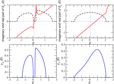
In the case of the metal, the condition corresponds to the maximum of the density of states, which represents a very broad resonance. In the case of the semiconductor we see that in the gap we have , with real, thus corresponding to a pole in the Green’s function and, therefore, representing a surface or Tamm state. Let us calculate the wave function of the Tamm state (for simplicity we consider the case ). The general wave function has the form
| (40) |
where and are position-base states at the sites of the chain, and and are the corresponding amplitudes. The matrix elements of the Hamiltonian, and leads to
| (41) | |||
| (42) |
where is the Heavyside function, with . The above equations are subject to the boundary condition . We now make the observation that for , there is a non trivial solution for the amplitudes given by the recursive relation
| (43) |
and all . The wave function of the surface state is therefore given by
| (44) |
with obtained from the normalization of the wave function. Clearly, for the surface state to exist we need , the case we used in our numerical calculations. For the surface state is absent. In the particular case a Shockley state will develop in the gap, which is not a surface state. Also for the metal there are some conditions where localized states can form at the surface. Let us take the semi-infinite one-dimensional metal introduced in Fig. 1, whose Hamiltonian reads
| (45) |
and we have assumed all the hoppings equal. Proposing a localized wave function of the form
| (46) |
and writing the Schrödinger equation as
| (47) | |||||
| (48) |
we obtain for the energy of the localized state
| (49) |
with the solution of
| (50) |
Since must be larger than zero we must have and the energy of the localized state is
| (51) |
located below the bottom of the metal band. So, in this special condition it is possible for the metal to develop a localized state at the surface. If we generalize the above case and include the possibility that the hopping between the site and the site is , the wave function of the localized state has to be generalized to
| (52) |
and the Schrödinger equation has now the form
| (53) | |||||
| (54) | |||||
| (55) |
whose solution gives and
| (56) |
and the energy is still given by . Since we must have only some values of the parameters produce surface states, in particular we must have (which is not the case considered in the simulations.).
We now make finite coupling the semiconductor and the metal. In Fig. 3 we plot the imaginary and the real parts of for different values of .
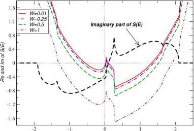
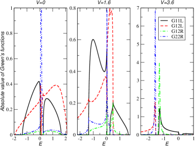
Because contains now contributions from both the imaginary parts of and there will be a finite imaginary part in the energy range of the semiconductor’s gap. As a consequence the Tamm state previously located in the gap becomes now a sharp resonance and is visible in the local density of states , as we show in Fig. 4.
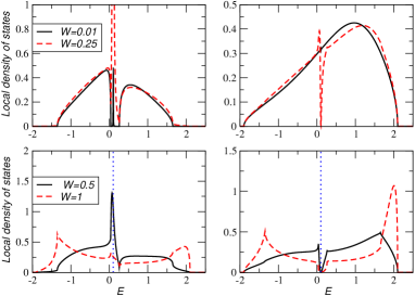
Of particular interest is the strong transfer of spectral weight from the density of states of the metal to the resonance in the semiconductor, given rise to an anti-resonance in the density of states of the metal. It is interesting that the high density of states persists where the resonance was located even when is no longer zero, albeit small. Only for large values of , such as , a large transfer of spectral weight to resonances at lower and higher energies takes place. From Fig. 3 we see that for moderate values of , even when we have , no sharp resonance appear in the local density of states because is very large at those points. For strong resonances appear at the lower and top edges of the bands.
4 Transport properties
We now study the non-equilibrium transport across the junction. This is done using the non-equilibrium Green’s function method keldysh . This method is particularly suited to study the regime where the system has a strong departure from equilibrium, such as when the bias potential is large. The system is however in the steady state. Since the seminal paper of Caroli et al. on non-equilibrium quantum transport Caroli , that the method of non-equilibrium Green’s functions become generalized to the calculation of transport quantities of nanostructures. There are many places where one can find a description of the method Ferry ; Datta ; Jauho , but an elegant one was recently introduced in the context of transport through systems that have bound states, showing that the problem can be reduced to the solution of a kind of quantum Langevin equation Sen .
The general idea of this method is that two perfect leads are coupled to our system, which is usually called the device. In our case the device is defined by the junction, a two site system, involving the and sites. The Green’s function of the device has to be computed in the presence of the leads. This corresponds to our Green’s function. Besides the Green’s function we need the effective coupling between the leads and the system (the junction) which are determined in terms of the self-energies as
| (57) |
therefore the effective coupling depends on the surface Green’s function of the perfect leads. According to the general theory the two leads are in thermal equilibrium at temperatures and chemical potential and are connected to the system at some time . The bottom line is that the total current through the device is given by (both spins included)
| (58) |
where the transmission is given by
| (59) |
Performing the trace we obtain
| (60) |
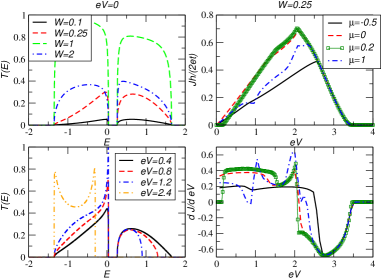
Because we are applying a bias voltage across the junction, we choose and . Also the electrostatic potential has to change continuously between the semiconductor and the metal. We choose that the variation of the potential is proportional to the distance to the electrodes, therefore the local energies in the junction have to be modified according to
| (61) |
The sites of the metal are shift by . Since is computed using and this depends on and on , will also be a function of the bias potential . The choice made in Eq. (61) corresponds to the solution of the discrete Poisson equation ignoring the charge fluctuations taking place to screen the external electric field. (In general terms, to determine the potential at sites and we would have to solve the Poisson equation coupled to the solution of the Schrödinger equation Hasegawa ; Yonemitsu , but the above transformation of and gives a good first approach to the exact result.) One technical aspect worth stressing here is the fact that, in general, non-linear transport should be done in a self-consistent way. This is the case in two situations: (i) when interactions (Coulomb or phonons, say) are taken into account; (ii) when the potential inside the conductor is relevant for transport. In the case we are considering here the conductor is reduced to a two-site system in the absence of interactions. Therefore, a self-consistent calculation is not needed.
Since the transmission function depends on the imaginary part of the surface density of states, the gap due to semiconductor shows up. From Fig. 5 we see that the current across the junction is only linear upon for very small values of the bias potential. As is further increased non-linearities in start to develop due to the energy dependence of , which is strongly influenced by the resonances shifting in energy as we vary the bias (see left down panel of Fig. 5); for large (say 2) the upper band of the semiconductor non longer contributes to the transport, due to the relative shift of the local density of states induced by . Also at large resonances develop in at both lower and higher energies; this effect is seen at the bottom left panel of Fig. 5 for eV. As the junction is strongly biased the current starts being suppressed due to the relative motion of the local energy of sites in the junction and the bands of the semiconductor. For large bias, the on-site energy of the junction’s sites moves to lower energies and these states are no longer available to the electrons coming from the semi-conductor. A qualitative model for tunneling across a one-site system also presents the general features seen for in Fig. 5, except that the effects due to resonances are not present Jauho . Naturally, when the chemical potential of the semiconductor lies on the gap it is necessary a finite bias voltage to produce a current.
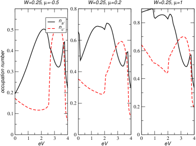
The average number of electrons, per spin, at the site of the device is given by
| (62) |
Specializing to the sites and we obtain
| (63) | |||
| (64) |
where the are the Fermi functions, and are defined as
| (65) | |||
| (66) |
From Figure 6 we see that the local electronic density at and sites is a highly non-linear function of the bias potential. This behavior can only be understood by looking at the behavior of the matrix elements of the junction Green’s function both as a function of energy and bias voltage. Clearly there are many resonances in the Green’s function matrix elements, which renders the analysis rather difficult. For small and intermediate bias voltage we have:
| (67) |
and
| (68) |
These inequalities are due to the relatively large value of relatively to . On the other hand, when the voltage increases, the above inequalities transform, roughly, into approximated equalities.
As a general trend, and will decrease at relatively large values of , due to the dependence of the energies and on (see Eq. (61)); this is specially the case for small coupling between the semiconductor and the metal (small ). In the case of small coupling, the contribution due to the off-diagonal Green’s function is small, since this latter quantity is proportional to and therefore its contribution to and (see Eq. (64)) is proportional to . So, in this case, the occupancy of the sites and is only due to the electronic wave-function coming from the system to which the corresponding site is directly connected.
For large bias voltage the matrix elements that contribute to develop large resonances which contribute to the increase of relatively to at eV.
It turns out that the details of the behavior of and depend some what on the relative strength of the hopping parameters and on-site energies.
5 Summary and conclusions
In this paper we have studied a simple one-dimensional model of semiconductor-metal junction. The advantage of this simplification is that all the features can be studied using analytical expressions. We have shown that the semi-infinite metal does generate surface states in particular conditions. For the semiconductor surface states can form in the gap. Resonances can be formed local density of states of the metal if the surface parameters are very different from those in the bulk. The energy position of such resonance is given by
| (69) |
In the case and , is simply the energy of the maximum of the local density of states.
When the interface is formed by making the parameter finite, the surface state formed in the gap of the semiconductor becomes a resonance, because the density of states of the metal is finite in the gap of the semiconductor. This is a consequence of the choice of the parameters for the semiconductor for the metal. We could as well have chosen a different set of parameters, such that the density of states of metal was zero in the gap of the semiconductor. In this case the surface state, as pole of the full Green’s function, would still survive as long as the renormalization of its energy due to the finiteness of the real part of the metal Green’s function would not move it away from the gap. As changes the resonances in the semiconductor and in the metal drift in energy
These resonances have a strong impact on the transport properties of the junction, because for fixed values of , their energy location is dependent on the bias voltage which changes the on-site energies of the atoms in the junction. Their effect is even more dramatic on the electronic occupancy of the atoms in the junction.
Although our system is a very simple one, the features seen in this case will also be present on more realistic cases. However, in the context of quasi one-dimensional organic conductors our calculations have direct relevance; for example, the electronic transport in a molecular wire will develop features as those described here close to the contacts to the metallic leads.
Acknowledgments
This work was supported by FCT under the grant
PTDC/FIS/64404/2006. The author acknowledges Ricardo M.
Ribeiro for a critical reading of the manuscript.
Appendix A Simple derivation of Eq. (13)
References
- (1) Harald Ibach, Physics of Surfaces and Interfaces, (Berlin: Springer, 2006).
- (2) I. Tamm, Phys. Z. Sowjetunion 1, 733 (1932).
- (3) Katsuyoshi Kobayashi, Phys. Rev. B 65, 035419 (2002).
- (4) Nikos Lazarides, George P. Tsironis, and Yuri S. Kivshar, Phys. Rev. E 77, 065601 (2008).
- (5) C. Caroli, R. Combescot, P. Nozieres, and D. Saint-James, J. Phys. C:Solid St. Phys., 4, 916 (1971); idem, ibidem, 4, 2598 (1971); idem, ibidem, 5, 21 (1972).
- (6) William R. Bandy and Arnold J. Glick, Phys. Rev. B 13, 3368 (1976); idem, ibidem, Phys. Rev. B 16, 2346 (1977).
- (7) Z. G. Yu, D. L. Smith, A. Saxena, and A. R. Bishop, Phys. Rev. B 56, 6494 (1997); Phys. Rev. B 59, 16001 (1999).
- (8) F. Hernandez-Ramirez, A. Tarancon, O. Casals, E. Pellicer, J. Rodriguez, A. Romano-Rodriguez, J. R. Morante, S. Barth, and S. Mathur, Phys. Rev. B 76, 085429 (2007).
- (9) P. Sautet and C. Joachim, Phys. Rev. B 38, 12238 (1988).
- (10) H. Mizes and E. Conwell, Phys. Rev. B 44, 3963 (1991).
- (11) P. A. Khomyakov, G. Brocks, V. Karpan, M. Zwierzycki, and P. J. Kelly Phys. Rev. B 72, 35450 (2005).
- (12) N. M. R. Peres and F. Sols, J. Phys.: Condens. Matter 20, 255207 (2008).
- (13) John Tomfohr and Otto F. Sankey, J. Chem. Phys. 120, 1542 (2004).
- (14) M. P. López Sancho, J. M. López Sancho, and J. Rubio, J. Phys. F: Met. Phys. 15, 851 (1985).
- (15) K. S. Dy, Shi-Yu Wu, and T. Spratlin, Phys. Rev. B 20, 4237 (1979).
- (16) James D. Brasher and K. S. Dy, Phys. Rev. B 22, 4868 (1980).
- (17) Nicholas J. Higham and Hyun-Min Kim, IMA J. Numer. Anal. 20, 499 (2000).
- (18) Aleksey Kletsov, Yuri Dahnovsky, and J. V. Ortiz, J. Chem. Phys. 126, 134105 (2007).
- (19) Aleksey Kletsov and Yuri Dahnovsky, Phys. Rev. B 76, 035304 (2007).
- (20) N. M. R. Peres, T. Stauber, and J. M. B. Lopes dos Santos, Phys. Rev. B 79, 035107 (2009).
- (21) L. P. Keldysh: Sov. Phys. JETP 20, 1018 (1065).
- (22) David K. Ferry and Stephen M. Goodnick, Transport in Nanostructures, (Cambridge: Cambridge University Press, 2001).
- (23) Supriyo Datta, Electronic Transport in Mesoscopic Systems, (Cambridge University Press: Cambridge, 2005).
- (24) Hartmut Haug and Antti-Pekka Jauho, Quantum Kinetics in Transport and Optics of Semiconductors, 2ed, (Springer: Berlin, 2008).
- (25) Abhishek Dhar and Diptiman Sen, Phys. Rev. B 73, 085119 (2006).
- (26) Kenji Yonemitsu, Nobuya Maeshima, and Tatsuo Hasegawa, Phys. Rev. B 76, 235118 (2007).
- (27) K. Yonemitsu, Mechanism of ambipolar field-effect transistors on one-dimensional organic Motts, Gunzi Saito, Fred Wudl, Robert Haddon, and Katsumi Tanigaki, Editors, Multifunctional Conducting Molecular Materials, (Royal Society of Chemistry: Cambridge, 2007), pp. 276; idem arXiv:0710.3533.