Using adiabatic coupling techniques in atom-chip waveguide structures
Abstract
Adiabatic techniques are well known tools in multi-level electron systems to transfer population between different states with high fidelity. Recently it has been realised that these ideas can also be used in ultra-cold atom systems to achieve coherent manipulation of the atomic centre-of-mass states. Here we present an investigation into a realistic setup using three atomic waveguides created on top of an atom chip and show that such systems hold large potential for the observation of adiabatic phenomena in experiments.
1 Introduction
Trapping and controlling small numbers of neutral atoms has, in recent years, emerged as one of the most active and productive areas in physics research [1, 2, 3, 4]. Such systems allow to perform experiments to answer fundamental questions in quantum mechanics [5, 6] and hold great potential for use in quantum information processing [7, 8, 9]. Advances in the technology of optical lattices and micro-traps have allowed for substantial progress in this area [10, 11, 12, 13, 14] and various concepts have been developed to prepare and process the states of single atoms. While techniques for controlling and preparing the internal states of atoms using appropriate electromagnetic fields are well developed, only a few concepts exist for achieving the same control over the spatial part of a wavefunction [15, 16, 17, 8, 18]. Such control would complement currently existing techniques and allow for the complete engineering of a particle’s quantum state.
One area where control over the spatial part of the wavefunction is important is the challenge of devising techniques for controlled movement of atoms between different regions in space. In optical lattices this corresponds to moving between discrete lattice sites and in waveguide settings this would allow transfer from one guide to another. Direct tunneling is a coherent process that can achieve this, however Rabi-type oscillations make it experimentally very hard to reach high fidelities [19].
Recently it was pointed out that systems consisting of three separated centre-of-mass modes allow for the use of STIRAP-like processes to achieve robust transfer of atoms from one position to another with high fidelity [16, 17, 20]. The process of Stimulated Raman Adiabatic Passage (STIRAP) is well known in three-level-optics, where it refers to the technique of applying a counter-intuitive sequence of laser pulses to achieve a transition of an electron between the two ground states in a -system [21, 22]. In the atom trap scenario the energy levels are replaced by spatially separated trap ground states and the laser interaction is replaced by the coherent tunneling interaction.
One advantage of adiabatic techniques is their large robustness against experimental uncertainties as long as the whole process is carried out mostly adiabatically [23]. However, this also means that a resonance between the asymptotic eigenstates has to exist, which is a condition that for many realistic situations is hard to ensure. Suggestions for and examinations of realistic systems in which the STIRAP process could be observed for cold atomic gases are therefore currently very rare.
In this work we will focus on atom-chip systems and investigate their suitability to observe this adiabatic process. These micro-fabricated chips, on which surface mounted, current carrying wires provide guiding potentials for matter waves, can be loaded with ultracold atom gases at low densities. As opposed to traditional experimental setups, these systems allow reaching smaller dimensions and the wire geometry, and therefore the waveguide geometry, can be chosen almost at will [24].
The first investigation into adiabatic techniques in waveguides was presented by Eckert et al. [17], who showed that a CPT-like process which acts like a 50:50 beam splitter could be realised with a large degree of fidelity. While the initial state for a numerical evolution can be prepared with a large degree of localisation, one of the problems following the subsequent evolution inside the waveguide is that the wavefunction disperses along the guide. This makes it hard to exactly measure the final state of the system and put a quantitative number on the efficiency of the adiabatic process. Here we will introduce a simple harmonic potential along the longitudinal direction of the trap, which will allow us to perfectly measure the fidelity of the process. It is also worth mentioning that STIRAP in optical waveguides with classical light has been observed recently [25].
In the next section we will first remind the reader by briefly reviewing the idea of STIRAP and its translation into the realm of waveguides. After that, in Section 3, we will examine a model waveguide potential in which the resonance condition is fulfilled throughout the whole process and show that the dispersion of the wavefunction in the longitudinal direction has no significant effect on the fidelity of the process. In Section 4 we describe a realistic situation by examining three waveguides created on top of an atom chip. We show that even though the resonance condition is not fulfilled at all times, a counter-intuitive approach will lead to larger transfer and can clearly be distinguished from a direct tunneling approach. Finally we conclude.
2 STIRAP
In this section we will briefly review the basic idea of STIRAP, which is a technique originally developed for transitions in optical -systems and which makes use of a two-photon Raman process. By applying the pump and the Stokes pulse in a counter-intuitive time-ordered way it leads to population transfer directly from one of the ground states to the other without any population ever being in the excited transitional state. In optical systems this inhibits spontaneous emission and is therefore often referred to as a dark-state technique.
The basic idea can be understood in the simple model of a three state system described by the Hamiltonian
| (1) |
where we have set the energies of the three asymptotic eigenstates to zero and the Rabi frequencies of the pump and the Stokes pulses are given by and , respectively. This Hamiltonian can be diagonalised and the eigenstate which is of interest to us here is the so-called dark state given by
| (2) |
where the mixing angle is given by . This angle describes how the the population is distributed between the two states and and it can be chosen by varying the strength of the pump and the Stokes pulse with respect to each other in time. In particular, if the intensity of the Stokes pulse increases before that of the pump pulse (counter-intuitive coupling scheme), one finds that all initial population in will be transferred to .
The fact that this process can be observed for trapped atoms was first pointed out by Eckert et al. [16]. The asymptotic eigenstates of the Hamiltonian (1) are then the spatial modes the atoms occupy and the time-dependent coupling is given by the tunneling strength between these modes. While the time-dependence of the tunneling strength can be achieved by temporally changing the distance or the barrier height between the individual states, an atom moving in a waveguide can also experience this as a function of travelled distance [17]. In the next section we will examine an example of this.
3 Model
The Schrödinger equation for the evolution of a wave-packet in a two-dimensional waveguide structure is given by
| (3) |
where is the mass of the atom. As the third dimension does not significantly contribute to the dynamics we are aiming to observe, the restriction of the above Hamiltonian to two dimensions is justified. In this section we will first examine the STIRAP process using an idealised potential in which the condition of resonance between the individual waveguides is fulfilled at any point. This will help us to illustrate the basic process and in particular highlight the influence of the longitudinal dimension. In Section 4 we will compare these results to realistic atom chip scenarios in which we will have to relax the resonance condition.
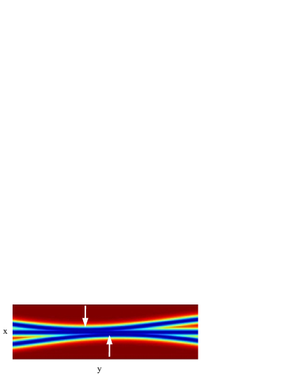
The assumption we make to guarantee that the ground state energy in all three waveguides is the same everywhere is that we can construct our potential by stitching three independent waveguides together. In a realistic situation the potentials creating each guide would influence each other and lead to non-symmetric situations between pairs. We assume each guide to have the potential
| (4) |
where determines the height, the width and the position of the minimum along the -axis. The overall potential is then assumed to be given by the minimum value of each of the three potentials at any point in space. A schematic view of the area in which the guides approach most closely is shown in Fig. 1.
The eigenstates of matter waves propagating in two-dimensional waveguides at different distances have recently been explored by Jääskeläinen and Stenholm [26]. They determined the conditions under which the movement of a matter wave can be considered adiabatic in a curved waveguide and developed a formalism based on localised and de-localised basis states. Here we will take a more straightforward approach and present a numerical solution to the process, which will show that despite the existence of velocity-dependent potentials due to the curvature of the waveguides [26] the STIRAP process can be observed with high fidelity.
Our simulations start with a well-localised wave-packet far away from the coupling area. In time, however, this packet will disperse along the waveguide, making it hard to quantify the success of the transfer process. To overcome this problem we introduce an additional harmonic potential of frequency along the -axis, which will lead to a refocussing of the wave-packet in the longitudinal direction after a time of . The initial state of our wave-packet is given by the ground state of an isotropic trap of the transverse frequency of the waveguide and its movement along the guide is induced by the harmonic potential as well.
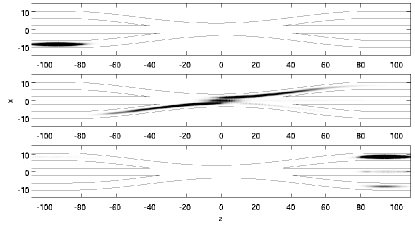
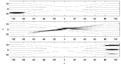
In Fig. 2 we show the evolution of the wavefunction at different times throughout the process for a counter-intuitive arrangement of the waveguides. Starting with the wave-packet located in the lower guide, one can clearly see that a majority of the probability is transferred into the upper guide. The evolution of the same initial state in an intuitive arrangement of waveguides (see Fig. 2) shows significantly less transfer.
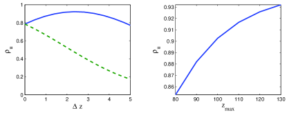
The amount of transfer varies as a function of several parameters. The first one is the distance between the two points of closest approach of the outer waveguides to the middle one, . We show the amount transfered as a function of this quantity in Fig. 4 on the left hand side. The full line (blue) represents the counter-intuitive case and a maximum at a finite value of is visible. The broken line shows the same quantity for the intuitive setting, clearly indicating that direct tunneling does not lead to high fidelities.
The second parameter that plays an important role is the degree of adiabaticity of the process. For a waveguide system this translates into the velocity with which the atom moves or alternatively the length of the coupling area. Here we keep the velocity effectively constant and show on the right hand side of Fig. 4 the variation of the maximum amount transfered as a function of the overall length of the coupling area. Making the overall structure longer also corresponds to decreasing the curvature of the waveguides and thereby reducing the velocity-dependent couplings introduced by it [26]. As expected we find that a more adiabatic process leads to a larger transfer probability.
Two caveats have to be pointed out with respect to the above simulations. While our calculations are carried out with the atom in the ground state in the transversal direction, this is not a necessary condition. In fact, the process will work for any state for which three degenerate asymptotic states exist. This in particular includes states of higher energy.
Secondly, our simulations are carried out only for the linear case of a single atom. If one would like to carry out the same process using, say, a Bose-Einstein condensate, one has to take care of the non-linearity that arises from the atomic interactions. However, we believe that our simulations give a very good approximation for low density condensates or even thermal clouds of atoms.
4 Atom Chips
While the above results clearly demonstrate the viability of the process, it is currently not clear in which experimental system it will be possible to observe it. One of the problems is that the asymptotic eigenstates of the system have to be in resonance at any point in time. This is hard to achieve in many realistic systems as neighbouring trapping potentials usually strongly influence each other when they are close enough to allow for significant tunneling rates.
Atom chips are well developed experimental tools these days and consist of an arrangement of current carrying wires mounted on a surface [24]. A current, , flowing through a wire creates a magnetic field around it with the minimum sitting on the wire. When applying a homogeneous bias field, , in the direction orthogonal to the wire, a two-dimensional field minimum above the wire can be created at a height given by [24]
| (5) |
To lift the energetic degeneracy between trapped and untrapped spin states and thereby avoiding spin flip losses at the field minimum, it is necessary to apply a second small -field component, , along the axis of the wire (z-axis). This changes the potential at the minimum from linear to harmonic [24]
| (6) |
where and the radial harmonic trap frequency is
| (7) |
We simulate the STIRAP process by considering three such wires separated by a distance of 9 initially. The overall length of the coupling zone chosen such that in the intuitive case several Rabi oscillations can be expected and the distance between two wires at the point of closest approach is chosen as 4.5. The applied bias field has a magnitude of and because of the small curvature of the wires can be regarded as orthogonal at any point. Since a large ground state is advantageous for tunnelling the atomic species we consider is 6Li.
In general the central minimum will be influenced by the fields from the two outer wires and increasingly so as the wires come closer. This will effect the resonance condition and ultimately prevent the STIRAP process from working. In order to minimize this behaviour we make use of a trick and adjust the current going through the middle wire to be slightly lower than the ones going through the outer wires. In our simulations we choose mA for the middle wire and mA for the two outer wires.
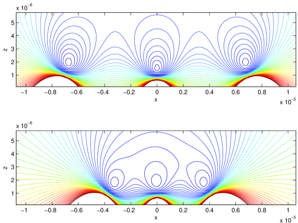
Fig. 5 shows the potential above the wires for the two different situations of symmetric distance between all wires (upper graph) and when the left wire is closer to the centre one than the right wire (lower graph). While an asymmetry in the second case is clearly visible, its effect on the potentials is moderate.
A full 3D simulation of the STIRAP process in these potentials is a numerically taxing task and beyond our current capabilities. We have therefore simulated the process by using the two-dimensional potentials of the kind displayed in Fig. 5 and changing the distance between the wires as a function of time. In doing so we neglect the dispersion of the wavefunction along the longitudinal direction. However, since we have shown in Section 3 that the dispersion does not have any significant effect on the transfer fidelity, our simulations can be seen as a good approximation to the full situation.
In Fig. 6 we show the results of these simulations by displaying the populations in the individual traps as a function of time for the intuitive (right) and the counter-intuitive case (left). Initially all population is on the left hand side and it can be clearly seen that in the counter-intuitive situation there is a smooth transition over to the right hand side. While in the perfect STIRAP setup no population should ever appear in the central trap, the various imperfections of this realistic example lead to a finite occupation during the process. However, at the very end no population is left in the middle trap. Contrary to this, the graph for the intuitive case shows Rabi oscillations between neighbouring waveguides and a less than full transfer of the wavefunction. These are two signs that would allow to distinguish adiabatic transfer from simple tunneling.
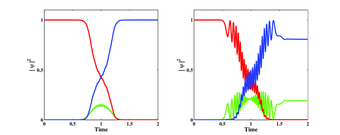
The fact that we achieve higher transfer fidelities in this non-perfect situation compared to the results presented in Section 3 is purely due to being able to evolve more adiabatically in time than in space due to the limitations of our computer hardware.
5 Conclusion
We have investigated the use of the STIRAP technique to transfer atomic wave-packets between neighbouring waveguides. Using an idealised system, we have first shown that the dispersion along the guide does not significantly affect the transfer probability. This was done by introducing a harmonic potential along the longitudinal axis, which allowed to refocus the wave-packet after half an oscillation period. We have then simulated the STIRAP process using realistic potentials created above current-carrying wires on atom chips and shown that by chosing a lower current for the central wire the energetic resonance condition can be fulfilled at any point to a very high degree. The results clearly showed that adiabatic transfer in the counter-intuitive setup leads to a higher fidelity and can be clearly distinguished from direct tunneling in the intuitive setup by the absence of Rabi oscillations.
References
References
- [1] Hänsel W, Reichel J, Hommelhoff P, and Hänsch TW, Phys. Rev. A 64 063607 (2001).
- [2] Bergamini S, Darquié B, Jones M, Jacubowiez L, Browaeys A, and Grangier P, J. Opt. Soc. Am. B 21, 1889 (2004).
- [3] Chuu C-S, Schreck F, Meyrath TP, Hanssen JL, Price GN, and Raizen MG, Phys. Rev. Lett. 95, 260403 (2005).
- [4] Shevchenko A, Heiliö M, Lindvall T, Jaakkola A, Tittonen I, Kaivola M and Pfau T, Phys. Rev. A 73, 051401(R) (2006).
- [5] Eschner J, Raab C, Schmidt-Kaler F, and Blatt R, Nature 413, 495 (2001).
- [6] Beugnon J, Jones MPA, Dingjan J, Darquié B, Messin G, Browaeys A, and Grangier P, Nature 440, 779 (2006).
- [7] Brennen GK, Caves CM, Jessen PS, and Deutsch IH, Phys. Rev. Lett. 82, 1060 (1999).
- [8] Jaksch D, Briegel H-J, Cirac JI, Gardiner CW, and Zoller P, Phys. Rev. Lett. 82, 1975 (1999).
- [9] Jaksch D, Cirac JI, Zoller P, Rolston SL, Côté R, and Lukin MD, Phys. Rev. Lett. 85, 2208 (2000).
- [10] Birkl G, Buchkremer FBJ , Dumke R, and Ertmer W, Opt. Comm. 191, 67 (2001).
- [11] Khudaverdyan M, Alt W, Dotsenko I, Förster L, Kuhr S, Meschede D, Miroshnychenko Y, Schrader D, and Rauschenbeutel A, Phys. Rev. A 71, 031404(R) (2005).
- [12] Yavuz DD, Kulatunga PB, Urban E, Johnson TA, Proite N, Henage T, Walker TG, and Saffman M, Phys. Rev. Lett. 96, 063001 (2006).
- [13] Sortais YRP, Marion H, Tuchendler C, Lance AM, Lamare M, Fournet P, Armellin C, Mercier R, Messin G, Browaeys A, and Grangier P, Phys. Rev. A 75, 013406 (2007).
- [14] Fortier KM, Kim SY, Gibbons MJ, Ahmadi P, and Chapman MS, Phys. Rev. Lett. 98, 233601 (2007).
- [15] Zhang M, Zhang P, Chapman MS, and You L, Phys. Rev. Lett. 97, 070403 (2006).
- [16] Eckert K, Lewenstein M, Corbalán R, Birkl G, Ertmer W, and Mompart J,Phys. Rev. A 70, 023606 (2004).
- [17] Eckert K, Mompart J, Corbalán R, Lewenstein M and Birkl G, Opt. Comm. 264, 264 (2006).
- [18] Karski M, Förster L, Choi J-M, Steffen A, Alt W, Meschede D, and Widera A, Science 325, 174 (2009).
- [19] Mompart J, Eckert K, Ertmer W, Birkl G, and Lewenstein M, Phys. Rev. Lett. 90, 147901 (2003).
- [20] Greentree AS, Cole JH, Hamilton AR and Hollenberg LCL 2004, Phys. Rev. B 70 235317.
- [21] Bergmann K, Theuer H, and Shore BW, Rev. Mod. Phys. 70, 1003 (1998).
- [22] Vitanov NV, Fleischhauer M, Shore BW, Bergmann K, Adv. At., Mol., Opt. Phys. 46, 55 (2001).
- [23] Härkönen K, Kärki O, and Suominen K-A, Phys. Rev. A 74, 043404 (2006).
- [24] Folman R, Krüger P, Schmiedmayer J, Denschlag J and Henkel C 2002 Advances In Atomic, Molecular, and Optical Physics 48 263–356
- [25] Longhi S, Della Valle G, Ornigotti M, and Laporta P 2007 Phys. Rev. B 76, 201101(R).
- [26] Jääskeläinen M and Stenholm S, Phys. Rev. A 68, 033607 (2003).