Photon scattering by a three-level emitter in a one-dimensional waveguide
Abstract
We discuss the scattering of photons from a three-level emitter in a one-dimensional waveguide, where the transport is governed by the interference of spontaneously emitted and directly transmitted waves. The scattering problem is solved in closed form for different level structures. Several possible applications are discussed: The state of the emitter can be switched deterministically by Raman scattering, thus enabling applications in quantum computing such as a single photon transistor. An array of emitters gives rise to a photonic band gap structure, which can be tuned by a classical driving laser. A disordered array leads to Anderson localization of photons, where the localization length can again be controlled by an external driving.
pacs:
03.67.-a, 42.50.Ex, 42.50.Gy1 Introduction
The effects of spontaneous emission have been extensively explored in two limits. In the weak coupling limit, spontaneous emission is essentially viewed as irreversible loss and a source of decoherence. On the contrary, excitations are periodically exchanged between an emitter and the modes of a cavity in the regime of strong coupling. A different regime is explored in one-dimensional waveguides, where photon scattering is goverend by the interference of the absorbed, reemitted and the directly transmitted wave. For a simple two-level emitter this leads to a complete reflection if the photon is resonant with the atomic transition [1, 2, 3]. In the present paper we discuss photon scattering from a three-level emitter, which can lead to even richer structures in reflection and transmission.
In order to reach the one-dimensional regime, the coupling to the waveguide has to be strong compared to transversal losses. The strong coupling regime has been first realized in a high–Q resonator for optical or microwave photons (see, e.g. [4, 5]). Later, strong coupling was also demonstrated in nanoscale integrated devices using photonic crystal microcavities [6, 7]. In such a cavity, however, the emitter couples only to a discrete set of modes and not to a one-dimensional continuum as in a waveguide. Great advances to reach the regime of strong coupling also in this situation have been reported only recently using several different systems such as photonic crystal waveguides [8], tapered optical fibers [9] or hollow core fibers [10]. Another opportunity is to exploit the strong localization of surface plasmon polariton (SPP) modes along a metallic nanowire [11, 12, 13, 14]. Strong coupling seem to be feasible even in free space if the photons are focussed appropriately [15]. Some of these different setups have been sketeched in figure 1. Thus the peculiar effects discussed in the present paper may become experimentally accessible in the near future.
In the present paper we solve the scattering problem for photons in one-dimensional waveguides coupled to a single three-level emitter in various configurations (cf. figure 2). It is shown that a waveguide coupled to a -type emitter or a driven -type emitter shows a characteristic EIT-like transmission and reflection spectrum. Raman scattering occurs for a -type emitter. Most remarkably, the Raman scattering amplitude can be turned to one on resonance, so that the photon is deterministically transferred to a sideband, flipping the quantum state of the emitter. These features allow for a variety of applications in quantum optics and quantum information. A possible realization of a single photon transistor from a driven emitter is discussed in section 4.1. The transmission through a regular array of emitters is discussed in section 4.2. It is shown that the resulting photonic Bloch bands are widely tunable with an external classical control field. Disorder in the emitter positions leads to Anderson localization of the photonic eigenstates, where the localization length can also be controlled by the external field as shown in section 4.3.
2 Single photons in nanoscale waveguides

In this section we solve the scattering problem for a photon in a quasi one-dimensional geometry as sketched in figure 1. The dynamics is governed by two effects which are usually not present in free space, the strong coupling to a single emitter and the interference of spontaneously emitted waves. In particular, the dynamics in such a one-dimensional waveguide is modelled by the Hamiltonian [1, 16, 17]
| (1) |
The free propagation of the photons is described by the Hamiltonian
| (2) |
Here, and denote the annihilation operators of a right- or left-moving photon at position , respectively. The separation into left- and right-moving modes is possible as we are dealing with optical photons with a frequency width much smaller than the mean frequency . Thus one can safely decompose the field into two distinct contributions with positive and negative wavenumbers, corresponding to right- and left-moving modes. The interaction Hamiltonian is local at the position of the emitter , and is given by
| (3) |
where and denote atomic lowering and raising operators, respectively. We will consider different structures of the emitter described by different Hamiltonians , which will be specified for the respective situations below. In the following we set , thus measuring all energies in frequency units.
The dynamics is simplified by setting the coordinates such that and introducing the (anti)-symmetric modes
| (4) |
so that the Hamiltonian for the symmetric mode reads
| (5) |
with while the antisymmetric-mode does not couple to the emitter at all. In the following we consider only the symmetric mode and thus drop the index .
Then it is easy to show that the rate of spontaneous emission into the one-dimensional waveguide is given by . Below we mostly use to characterize the interaction strength. Spontaneous emission to other modes out of the one-dimensional waveguide is modelled by attributing an imaginary part to the energies of the excited levels in in the spirit of the quantum jump picture [18, 19].
A more efficient coupling may be realized by placing the emitter at one end of a semi-inifinite waveguide instead of side-to-side. This was shown in particular for plasmonic waveguides [12], where the electric field strength around a nanotip is significantly incresed (cf. figure 1 (b)) The propagation of the right- and left-going modes is then restricted to . In this case we introduce the mode function
| (6) |
such that describes the incoming and the reflected photons. The original Hamiltonian (1) then also assumes the form (5), however with .
The basic scattering problem for a simple two-level emitter has been solved by Shen and Fan [1]. In this case we have and , where denote the respective Pauli matrices. The solution starts from an eigenstate of the full Hamiltonian which can be written as
| (7) |
where and are the ground and excited state of the emitter, respectively. Here and in the following denotes the state of zero photons, i.e. the empty waveguide. The mode function is discontinuous due to the -function in the interaction Hamiltonian,
| (8) |
Using the Lippmann Schwinger formalism one can then rigorously show that an input state given by the mode function is scattered to an output state given by the mode function [16]. In particular one finds that the transmission amplitude for a monochromatic input state with wavenumber is given by
| (9) |
This procedure is readily generalized to three-level emitters, but some attention has to be paid in the case of two groundstates, i.e. a -type atom as shown in figure 2 (B).
3 Scattering by a three-level atom
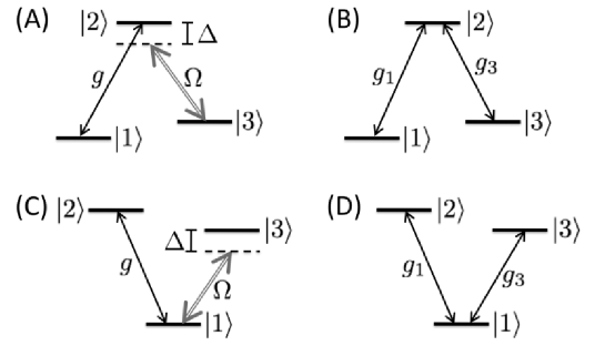
In this section we solve the scattering problem for a single photon and a three-level emitter with three internal states. The different possibilities for the coupling and a classical driving field are sketched in figure 2.
3.1 Electromagnetically induced transparency in a driven -system
We start with the driven level scheme shown in figure 2 (A), where the excited atomic state is coupled to another level by a classical laser beam with Rabi frequency and detuning . Within the rotating wave approximation, the atomic Hamiltonian is given by
| (10) |
where we have set the energy scale such that the energy of level is zero. The interaction Hamiltonian is given by equation (5) with .
The eigenstates of the full Hamiltonian (1) are then given by
| (11) |
with eigenenergy . The coefficients are easily found to be
| (12) | |||||
where the transmission coefficient is given by
| (13) |
and denotes the Heaviside step function. An incoming photon with wavenumber in the -mode thus experiences a phase shift given by when it crosses the atom. The modulus of is smaller than one for or which describes transversal losses, i.e. the scattering of the photon out of the waveguide. In this case the emitter jumps incoherently to one of the ground levels and the photon is lost.
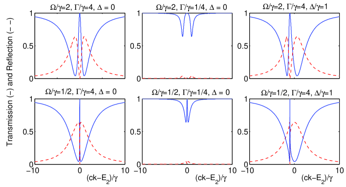
Let us first consider the case where level is metastable, i.e. . This situation is realized, for example, when the levels and are two hyperfine levels in the ground state manifold coupled by a radio-frequency driving field. Going back to left- and right-moving modes using equation (4), one finds that the transmission and reflection amplitudes of the waveguide are given by
| (14) |
The resulting transmission spectrum is depicted in figure 3 for different values of the parameters , and , showing the familiar EIT transmission spectrum [20]. The atom becomes fully transparent on the photon resonance, i.e. when the wavenumber is given by
| (15) |
The width of this central transpareny window is only given by the strength of the driving field . Furthermore the system is transparent for , where the incoming photon is far off-resonant and thus does not interact with the atom. In between we find dips of the transmission, whose width and depth increases with the coupling strength . These are mainly due to reflection if and due to losses otherwise. Complete reflection is only possible if the losses vanish exactly () and
| (16) |
where denotes the effective Rabi frequency. The complete spectrum is symmetric only for and asymmetric otherwise.

The waveguide can be fully transparent only if level is metastable. For there will always be losses such that . Figure 4 shows how the transmission spectrum changes when is increased: The transmission on resonance decreases until finally the EIT transparency window vanishes completely.
3.2 A -system with two coupling transitions
The -system shown in figure 2 (B), where both ground states couple to the waveguide mode is described by the atomic Hamiltonian
and the interaction Hamiltonian
| (17) |
Now we have to take into account that the atom can be in state and when a photon is present. An arbitrary state with one excitation can thus be written as
| (18) |
The eigenstates of the full Hamiltonian are found by substituting this ansatz into the time-independent Schödinger equation. Then one finds two types of solution:
The continous solution is characterized by a destructive interference of the functions and at the position of the atom so that this mode does not interact. The solution is thus given by
| (19) |
with the normalisation factor . The wavenumbers are related to the eigenenergy by and .
The other solution is discontinuous due to the interaction with the atom. One finds that
| (20) |
with the transmission coefficient
| (21) |
where are the spontaneous emission rates into the waveguide when the emitter decays into the respective atomic level.
Using these states, one can easily solve the scattering problem. We find that an incoming photon with wavenumber is scattered depending on the atomic state according to
| (22) | |||||
where is the energy difference between the two ground states.
A remarkable result is that a resonant photon can be absorbed deterministically as pointed out in [2] for the case . Suppose the emitter is initially prepared in the ground state and the coupling constants satisfy the condition . The transmission amplitude is then given by and the internal state of the emitter is flipped,
| (23) |
as long as the photon is not lost. If transversal losses are absent, i.e. , the scattering process realizes a deterministic quantum gate between a photon and a single emitter. However, the described protocol is also very useful in the case , when a significant fraction of the incident photons is lost. If a single photon is measured in the output, the gate is known to have operated successfully. Combined with error-proof quantum communication schemes [21, 22, 23], this provides a powerful building block for quantum computing purposes. We will discuss the realization of a single photon transistor using this property in section 4.1.
3.3 Driven V-type atom
Next we consider the situation shown in figure 2 (C), where the classical driving field couples the ground state to the excited state , so that the atomic Hamiltonian is now given by
| (24) |
The interaction Hamiltonian is given by equation (5) with . The state is assumed to be stable, for instance the states and can be two hyperfine levels coupled by microwave radiation.
The situation is best dealt with in a dressed state picture, introducing the eigenstates of the atomic Hamiltonian
with eigenenergies
| (26) |
The atomic and interaction Hamiltonians are then given by
| (27) |
with
| (28) |
This is exactly the situation depicted in figure 2 (B), which has been discussed in the previous section. However, a driven system has the enormous advantage that system parameters such as the ration can be tuned to almost any desired value by choosing an appropriate classical control field. In particular, this can be used to implement a single photon transistor as shown in section 4.1.
Using the result from the previous section, one finds that an incoming photon with wavenumber is scattered according to
| (29) | |||||
where is the energy difference between the two dressed states. The transmission phase factor is given by
| (30) |
3.4 A V-type atom with two coupling transitions
This case, depicted in figure 2 (D), is equivalent to case A in the dressed state picture as long as loss can be neglected. In the general case one has to be a bit more careful, because the loss terms are also changed by a transformation to the dressed state basis. Thus we also give the full solution for the case of a V-type atom with two coupling transitions in the following.
We consider the atomic Hamiltonian
| (31) |
where we have set the energy scale such that the energy of level is zero. The interaction Hamiltonian is given by
| (32) |
The eigenstates of the full Hamiltonian can then be written as
| (33) |
with eigenenergy . The coefficients are easily found to be
where the transmission coefficient is given by
| (34) |
An incoming photon with wavenumber in the -mode thus experiences a phase shift given by when it crosses the atom. The reflection and transmission amplitudes for the left- and right-moving are again given by equation (14). The atom can become fully transparent only if one of the levels or is metastable and the photon is resonant to the atomic transition between the metastable and the ground level:
| (35) |
4 Applications
Having solved the basic scattering problem, we now go on to discuss various applications of these results.
4.1 A single photon transistor
A single photon transistor is a universal nonlinear element with wide-ranging application from classical telecommunication to quantum computing [24, 17]. However, it is very hard to realize since photons rarely interact directly, so that the necessary interactions must be mediated by matter in a deterministic way.
The basic idea of this transistor is that a waveguide strongly coupled to a single emitter is either reflective or transparent, depending on the state of the emitter. The state can then be switched by a single gate photon. Previously, a realization of such a device in nanoscale one-dimensional waveguides has been proposed [17]. A disadvantage of this method is that it requires a precise timing between the quantum gate photon and a classical control pulse. Here we present an alternative approach which removes this restriction.
This single photon transistor works as follows: Consider the situation sketched in figure 2 (C), whose scattering properties have been analyzed in section 3.3. Initially the system is in state and the classical control field is off . Now the emitter is driven to the state by an adiabatic passage technique, slowly increasing and possibly varying the Laser frequency so that finally a situation with and is reached. Several methods for this procedure were demonstrated experimentally (see, e.g., [25]). After this initialisation procedure, the transistor is sensitive to the arrival of the gate photon as long as the driving field remains on. If one is injected, it scatters according to equation (29). As we have prepared the emitter such that we have . Assuming that the photon is resonant, , the transmission coefficient is given by as long as losses can be neglected. Thus the internal state of the emitter is changed during the scattering process according to
After the scattering process, the initialisation sequence is reversed, mapping back to and to . Thus the state of the emitter is switched from to if and only if a gate photon has crossed the waveguide. As the external field is now switched off, , the scattering is essentially that of a two-level emitter. As shown in [1], the waveguide is reflective if the emitter is in state . If it has been switched to state by the gate photon, it is essentially decoupled – the waveguide is transparent. It should be noted that this procedure does not need a precise timing. The initialisation and de-initialisation sequences must be performed well before and well after the gate photon passed but the precise time does not play a role. Furthermore, the de-initialisation is performed by an adiabatic passage, which is more robust than procedures relying on Rabi flopping.
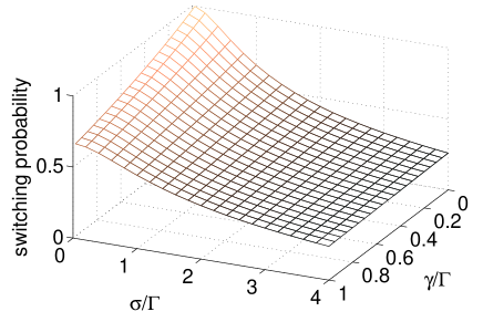
In the description of the basic idea we neglected losses and assumed a perfect resonance. Let us now consider a more realistic situation and calculate the switching probability for a general input state
| (36) |
In particular we consider a Gaussian input pulse
| (37) |
at resonance with the transition . Assuming that the adiabatic passage to the dressed state works perfectly the switching probability is then given by the probability to find the emitter in state after the scattering:
| (38) |
The first term gives the norm of the contribution of in the scattering state (29), weighted by the pulse shape of the gate photon and using . The second contribution is the probability that the emitter decays to level when the gate photon is lost by spontaneous emission to the outside world, where the branching ratio is . This switching probability is plotted in the case as a function of the width of the input pulse and the loss rate in figure 5.
4.2 Tunable photonic band gaps
Let us now consider the properties of a periodic array of emitters as shown in figure 6. The emitters are driven by a classical laser field in the EIT configuration shown in figure 2 (A). The strength and detuning of this driving then allows to tune the transport properties of the array.
Let us first consider the lossless case . The amplitudes of the right- and left- going waves in this array are then related by
| (39) |
where
| (40) |
is the transfer matrix (cf. [26]) Here, denotes the periodicity of the emitter array and the transmission and reflection coefficients defined in equation (14) have been used. The eigenvalues of the transfer matrix characterise the transport properties of the array. Since the product of both eigenvalues is always one, the eigenvalues are either complex conjugate numbers of magnitude one () or they are inverse of each other with magnitudes smaller and larger than one. The first case characterizes a photonic Bloch state with quasi momentum , so that transport is possible. In the latter case transport is impossible, i.e. lies in a band gap.
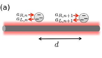
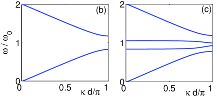
Examples of the resulting photonic Bloch bands are shown in figure 6. For (no driving) one recovers the Bloch bands well known for simple two-level emitters [1], with a band gap at the resonance frequency. For however, the upper level splits into two dressed states which both give rise to a Bloch band. The position and width of these bands is then tunable through and .
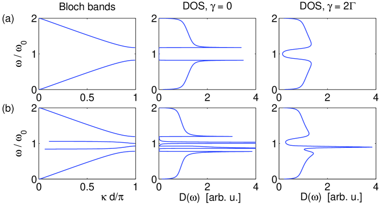
In a realistic system, the coupling to the waveguide will not be perfect and transversal losses by spontaneous decay from the excited state cannot be neglected. Then the transfer matrix is no longer unitary and its eigenvalues are rather given by , where gives the absorption coefficient. The effect of losses on the photonic band gap structure is illustrated in figure 7, where we compare the density of states with and without transversal losses. In the lossless case, the density of states is essentially given by . For , every state is broadened, so that the density of states is rather given by
| (41) | |||||
This definition of the density of states is adapted to the modification of the spontaneous emission rate of a single emitter in a photonic crystal structure [27]. Here, denotes the coupling matrix element of the emitter to a Bloch state with quasi momentum . As the interaction with the waveguide is local at the position of the emitter (cf. equation (3)), the coupling is simply given by the magnitude of the Bloch wave function at the position :
| (42) |
In the following example we chose , i.e. we consider the emission of a single impurity atom placed in the middle between two emitters forming the photonic band gap structure.
Figure 7 shows that the density of states around the resonance frequency is strongly modified around the resonance frequency by the external driving field. These features are still very pronounces in the case of strong transversal losses, i.e. large values of . This can be utilized, for instance, in order to manipulate the emission rate of a single impurity atom coupled to the waveguide simply by tuning the strength of the external driving laser (cf. [27, 28]).
4.3 Tunable Anderson localization of photons
In the previous section we considered transport of photons through a waveguide coupled to an array of emitters in a perfectly periodic configuration. If this periodicity is disturbed by disorder, as it will commonly be in real experiments, there are generally no infinitely extended Bloch states any more. Instead, every photonic wavefunction undergoes Anderson localization [29]. This localization was demonstrated experimentally in different systems [30, 31]. The localization transition is well understood for systems described by transfer matrices [26] such as (40). Here we consider an array of emitters where the distance between the emitters differs from site to site, in particular assuming a uniform distribution in the interval , where is the free-space wavelength of a photon with frequency . The transfer matrix of a whole array of emitters is then given by the product and its eigenvalues can be written as . The localization length characterises the spatial extend of a photonic wavefunction and measures the localization strength.
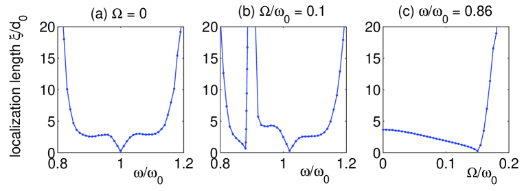
An example is shown in figure 8 for an array of three-level emitters in the EIT configuration as shown in figure 2 (A). We restrict ourselves to the lossless case and set , where is the atomic resonance frequency. The localization length is plotted as a function of the frequency of the incoming photons as obtained from a Monte Carlo simulation. The transfer matrix has been computed using randomly chosen values for the distance and diagonalized. The obtained values for the localization constant have been averaged over 100 realizations. Without external driving (figure 8 a), one observes the localization spectrum of a single two-level emitter. On resonance all emitters are completely reflective so that the localization length tends to zero. The introduction of a classical driving field changes the localization properties dramatically (cf. figure 8 b). The upper state splits into two dressed states, so that there are two resonance frequencies for which the emitters are fully reflective and hence . On the other hand becomes infinite when the EIT condition is fulfilled, as all emitter are fully transparent then.
5 Conclusion and Outlook
In the present paper we have solved the scattering problem for a single photon in a one-dimensional waveguide coupled to a three-level emitter. Several different configurations were taken into acount. Electromagnetically induced tranparency is observed for a driven -system and -system if both transitions couple to the waveguide. On the contrary, scattering to sidebands occurs for a driven -system and -system with two coupling transitions.
The control gained by the classical driving field pave the way for a variety of application from classical optics to quantum information. The control over the transmission in the EIT scheme can be used to taylor the optical properties of an array of emitters. Thus one can readily engineer photonic band gap structures or tune the localization length in disordered systems. The driven -system can be applied in a single photon transistor. The gate photon is scattered to a sideband changing the internal state of the emitter and thus switching the waveguide from reflective to transmittive.
Acknowledgements
Financial support from the Deutsche Forschungsgemeinschaft via the research fellowship programme (grant number WI 3415/1) and the Villum Kann Rasmussen foundation is gratefully acknowledged.
References
References
- [1] Shen J T and Fan S 2005 Opt. Lett. 30 2001
- [2] Pinotsi D and Imamoglu A 2008 Phys. Rev. Lett. 100 093603
- [3] Zumofen G, Mojarad N M, Sandoghdar V and Agio M 2008 Phys. Rev. Lett. 101 180404
- [4] Thompson R J, Rempe G and Kimble H J 1992 Phys. Rev. Lett. 68 1132
- [5] Brune M, Schmidt-Kaler F, Maali A, Dreyer J, Hagley E, Raimond J M and Haroche S 1996 Phys. Rev. Lett. 76 1800
- [6] Reithmaier J P, Sek G, Löffler A, Hofmann C, Kuhn S, Reitzenstein S, Keldysh L V, Kulakovskii V D, Reinecke T L and Forchel A 2004 Nature 432 197
- [7] Yoshie T, Scherer A, Hendrickson J, Khitrova G, Gibbs H M, Rupper G, Ell C, Shchekin O B and Deppe D G 2004 Nature 432 200
- [8] Faraon A, Waks E, Englund D, Fushman I and Vučković J 2007 Appl. Phys. Lett. 90 073102
- [9] Dayan B, Parkins A S, Aoki T, Ostby E P, Vahala K J and Kimble H J 2008 Science 319 1062
- [10] Bajcsy M, Hofferberth S, Balic V, Peyronel T, Hafezi M, Zibrov A S, Vuletic V and Lukin M D 2009 Phys. Rev. Lett. 102 203902
- [11] Chang D E, Sørensen A S, Hemmer P R and Lukin M D 2006 Phys. Rev. Lett. 97 053002
- [12] Chang D E, Sørensen A S, Hemmer P R and Lukin M D 2007 Phys. Rev. B 76 035420
- [13] Akimov A V, Mukherjee A, Yu C L, Chang D E, Zibrov A S, Hemmer P R, Park H and Lukin M D 2007 Nature 450 402
- [14] Hakala T K, Toppari J J, Kuzyk A, Pettersson M, Tikkanen H, Kunttu H and Törmä P 2009 Phys. Rev. Lett. 103 053602
- [15] Hwang J, Pototschnig M, Lettow R, Zumofen G, Renn A, Götzinger S and Sandoghdar V 2009 Nature 460 76
- [16] Shen J T and Fan S 2007 Phys. Rev. A 76 062709
- [17] Chang D E, Sørensen A S, Demler E A and Lukin M D 2007 Nature Physics 3 807
- [18] Dalibard J, Castin Y and Mølmer K 1992 Phys. Rev. Lett. 68 580
- [19] Carmichael H J 1993 An Open Systems Approach to Quantum Optics (Berlin: Springer Lecture Notes in Physics)
- [20] Fleischhauer M, Imamoglu A and Marangos J P 2005 Rev. Mod. Phys. 77 633
- [21] van Enk S J, Cirac J I and Zoller P 1997 Phys. Rev. Lett. 78 4293
- [22] Sørensen A and Mølmer K 1998 Phys. Rev. A 58 2745
- [23] Witthaut D, Lukin M D and Sørensen A 2009, in preparation
- [24] Bouwmeester D, Ekert A and (eds) A Z 2000 The Physics of Quantum Information (Berlin Heidelberg New York: Springer Verlag)
- [25] Oberst M, Klein J and Halfmann T 2006 Opt. Comm. 264 463
- [26] Berry M V and Klein S 1997 Eur. J. Phys. 18 222
- [27] Yablonovitch E 1987 Phys. Rev. Lett. 58 2059
- [28] Lodahl P, van Driel A F, Nikolaev I S, Irman A, Overgaag K, Vanmaekelbergh D and Vos W L 2004 Nature 430 654
- [29] Anderson P W 1958 Phys. Rev. 109 1492
- [30] Wiersma D S, Bartolini P, Lagendijk A and Righini R 1997 Nature 390 671
- [31] Schwartz T, Bartal G, Fishman S and Segev M 2007 Nature 446 52