Effect of polar discontinuity on the growth of LaNiO3/LaAlO3 superlattices
Abstract
We have conducted a detailed microscopic investigation of [LaNiO3(1 u.c.)/LaAlO3(1 u.c.)]N superlattices grown on (001) SrTiO3 and LaAlO3 to explore the influence of polar mismatch on the resulting electronic and structural properties. Our data demonstrate that the initial growth on the non-polar SrTiO3 surface leads to a rough morphology and unusual 2+ valence of Ni in the first LaNiO3 layer, which is not observed after growth on the polar surface of LaAlO3. A newly devised model suggests that the polar mismatch can be resolved if the perovskite layers grow with an excess of LaO, which also accounts for the observed electronic, chemical, and structural effects.
Recently complex oxide ultra-thin films have been drawing enormous attention due to the possibility of stabilizing unusual quantum phases and building interface-controlled devices ahn06 ; Caviglia . Towards this goal, the problem of polar interfaces is of fundamental importance, since a polar crystal structure grown on a non-polar substrate would be unstable due to the depolarizing fields Ohtomo ; Noguera . To avoid this issue, some mechanism must set in to compensate the potential jump by forcing electronic, structural or chemical (non-stoichiometry) changes. In particular, the active work on the LaAlO3/SrTiO3 system hwang2 ; Hwang3 ; huijbenrev has suggested an electron transfer between atomic layers that decreases Ti valence by 0.5 at the expense of 0.5 charge in the terminating atomic plane. Additionally, an alloy effect has been observed at the interface Muller , and first-principles computations revealed a contribution of ionic displacements Pentcheva .
In this letter, we report on the microscopic observation of an unusual valence state of Ni2+ in ultrathin LaNiO3/LaAlO3 superlattices (SL) grown on non-polar (or weakly polar) (001) TiO2-terminated SrTiO3 (STO) substrates. This is in marked contrast to identical SLs grown on polar LaAlO3 (LAO), which always exhibit the 3+ valence of the bulk-like LaNiO3 (LNO). To clarify the origin of these phenomena, we have tracked the changes of the Ni valence as a function of the SL thickness and developed an experimental procedure to monitor and control the electronic state of a transition metal ion.
High-quality epitaxial LNO/LAO SLs were grown on (001) TiO2-terminated STO single crystal substrates by pulsed laser deposition with in situ monitoring by RHEED Kareev1 . To minimize induced defects, STO substrates were prepared by our recently developed chemical wet-etch procedure (‘Arkansas treatment’) Kareev2 . A complementary set of SLs were also grown on LAO single crystal substrates. Detailed spectroscopic information was acquired in the soft x-ray regime in both fluorescence yield (FY) mode and total electron yield (TEY) mode at the Ni L3,2 absorption edge at the 4ID-C beamline of the Advanced Photon Source, ANL. To obtain precise information on the Ni charge state, all spectra were aligned by simultaneously measuring a NiO (Ni2+) standard with the SLs. Synchrotron-based x-ray diffraction has confirmed the high structural quality and the full epitaxy of the SLs Kareev1 .
In order to maintain the morphological quality and achieve the layer-by-layer (LBL) growth of the single unit-cell thin SLs, we used a recently developed interrupted growth methodKareev1 ; Blank . This method consists of a rapid ablation and a prolonged delay between two successive unit cell layers. The usual oscillation of RHEED specular intensity (RSI) for each unit cell occurs within a short flux-on period seen as a sharp dip of RSI, followed by a further slow recovery (see inset in Fig. 1). While RSI would have a full recovery in the ideal LBL growth, this first layer grown on STO always exhibits a characteristic drop as seen in Fig. 1, regardless of whether the initial layer is LAO or LNO. This observation is also consistent with the rough initial growth of the polar layer on the non-polar STO surface ( polar mismatch) as corroborated by AFM imaging of the surface. Conversely, this phenomenon is absent during the initial growth on LAO, where a full recovery can be seen after the first deposited layer.
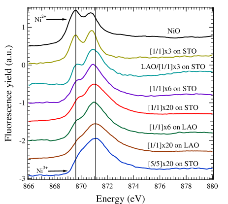
To elucidate the microscopic origin of this phenomenon, we performed resonant soft x-ray spectroscopy (XAS) on the Ni L3,2-edge. By using XAS, the Ni valence state can be directly fingerprinted for samples as thin as a single unit cell. By utilizing this exquisite sensitivity to the Ni charge state, we were able to detect and trace the effects of charge transfer, local symmetry and non-stoichiometry across the layers. Due to the overlapping La M4-edge, the spectrum at the Ni L3-edge is strongly distorted which is the reason for focusing on the Ni L2-edge. Fig. 2 shows the Ni L2 spectra measured in the bulk sensitive FY mode for the [LaNiO3(1 u.c.)/LaAlO3(1 u.c.)]N (SLs ([1/1]N thereafter) with a varying number of repeats, N, and different growth sequences. A thicker SL composed of 5 u.c. thick LNO layers is also included as a Ni3+ reference for a stoichiometric sample in the metallic phasePiamonteze . The bulk like Ni3+ valency of this superlattice was further confirmed by comparison with the bulk LaNiO3. By direct comparison of the absorption spectra in Fig. 2, the sharp difference between the Ni charge state in the [1/1]N SLs and the bulk like Ni3+ spectra can be seen.
A few important observations are due. First, the [1/1]3 sample with LNO grown directly on the STO surface clearly exhibits a characteristic doublet with a 0.3V shift to lower energy, which matches the Ni2+ XAS spectra of the NiO standard at the L2 edge. This implies that the initial growth results in a phase analogous to heavily oxygen deficient bulk LaNiO3-x Sanchez , such as LaNiO2.5 with a Ni valence of 2+. As N is further increased, the Ni valence for the SLs on STO moves progressively towards Ni3+ as noted by the difference between the 6-repeat and 20-repeat samples. This result implies that growing the polar SLs on a non-polar or weakly-polar substrate such as STO results in a massive chemical compensation and electronic reconstruction during the initial growth. In contrast, the XAS spectra for the same set of SLs grown on LAO show that Ni valence is very close to 3+ as directly evident from XAS on the SLs with N=6 and 20. To exclude the compensating charge transfer between Ti of STO and Ni of LNO, we compared the Ti L-edge spectrum in a TEY mode (not shown) to the Ti spectrum taken on a bare STO substrateKareev2 . The measurement unambiguously confirms that no significant change of Ti4+ valence takes place near the film-substrate interface, likely due to the high oxygen pressure during the deposition.
Next we investigated a possibility to preserve the fragile electronic state of Ni3+ ions by fabricating a series of SLs on a 2 u.c. LAO buffer layer deposited on STO. It is clear from the data shown in Fig. 2 for the N=3 SL with a LAO buffer that the buffer greatly aids in restoring the electronic state of Ni towards 3+.
Conductivity of bulk LNO has been shown to be sensitive to oxygen deficiency which tightly correlates with Ni valenceSanchez . To clarify if Ni2+ is connected to oxygen deficiency, we annealed the SLs at 900oC in flowing ultra-pure O2 at 1 Atm for 12 hours. Subsequent reduction in N2 followed by re-oxidation in O2 was carried out under the same conditions. DC resistivity measurements were performed after each step using a 4-terminal geometry. This experiment revealed that prolonged annealing in O2 of the as-grown samples has no sizable effect on the resistivity. In contrast, the reduction in nitrogen had strongly increased the resistivity of the samples by several orders of magnitude, while the subsequent re-oxidation successfully restored it back to the as-grown level, indicating that the conductivity is not related to simple oxygen deficiency. This experiment provides strong evidence that the observed deviation of Ni valency from 3+ is not due to insufficient oxidation during the deposition but is likely related to the formation of acceptor-like complex defects caused by the polar discontinuity.
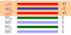
Fundamentally, the phase of a material deposited on the surface is determined by enthalpy, . While is controlled by the environmental thermodynamic parameters (e.g. pressure and temperature), it also intimately depends on the atomic interactions on the surface (i.e. wettability). Thus, the electrostatic interactions within a structure consisting of oppositely charged alternating atomic planes will result in a large increase to due to polar misfithwang2 , and render the structure unstable. Experimentally, the probability to grow such a structure from the vapor phase is negligibly small. Instead, it has been proposed that such a polar mismatch can be generally resolved by transferring 0.5 from the surface to the polar-nonpolar interfaceOhtomo ; Hwang3 . However, the experimental observation of the large amount of Ni2+ present in the ultra-thin SLs contradicts this model. To circumvent the issue, we propose that the presence of Ni2+ is likely associated with the polar compensation by the excess growth of an additional LaO plane. As illustrated in Fig. 4, at the initial stage of growth, this would result in a tri-layer structure like …/Ti4+O/La3+O2-/Ni2+O/La3+O2-, which contains a perovskite unit cell plus an extra LaO plane and remarkably possesses no total charge or dipole moment. Consequently, Ni is promoted to the 2+ charge state by the strong decrease of the electron potential due to the two LaO planes.
As the growth continues, the newly deposited [LaO/Ni(or Al)O2]m () layers must be accommodated by adjusting the plane charge densities (the charge per u.c. in units of ) of the bottom NiO2 plane and the surface plane. If the excess LaO plane remains on the surface, based on the charge neutrality and dipole compensationfootnote , one can show that its charge density equates to , while the Ni valence in the bottom NiO2 plane becomes . Note, setting to zero will correspond to the initial tri-layer structure. On the other hand, if the terminating plane is Ni(Al)O2, one can deduce that its charge density equates to with Ni valence in the bottom NiO2 plane being (here will correspond to a NiO2 plane deposited on the top of the tri-layer, and each of the following LaO/Ni(Al)O2 unit cells will increase by one). In either case, when , the charge density of the bottom NiO2 plane changes from -2 to -1.5, corresponding to the evolution of the Ni valence from 2+ to 2.5+ footnote1 . This model lends theoretical support for the observation that the valence of the N=6 SL is gradually approaching that of the N=20 with no sign of a static Ni2+ component footnote2 .
In practice, other mechanisms can certainly set in complicating the situation. In particular, non-stoichiometry such as atomic vacancies may play an important role. For instance, the electrostatic potential jump may decrease the enthalpy of formation of La vacancies in LaO planes and put related oxygen vacancies onto Ni(Al)O2 planes to reduce the dipole moment. Notice, the local field from the atomic vacancies is also capable of creating Ni2+ due to a small charge transfer energy of the Ni2+O- exciton. The precise correlation between the polarity problem and compensation by atomic defects requires further investigation.
In summary, by monitoring the Ni charge state as the control parameter, we have investigated the effect of polar mismatch on the electronic and structural properties of [1uc LNO/1uc LAO]N SLs. The initial growth stage is found to experience a structural reconstruction accompanied by marked changes of the Ni electronic structure. We suggest that to a large extent these results can be explained by the new tri-layer growth model, which corroborates the experimental data. Growing LAO buffer on STO is found to efficiently circumvent the polar mismatch issue and allows to preserve the electronically active Ni ions from changing the valence. These important findings are relevant for a wide range of complex-oxide materials and should pave a way to growth of novel ultra-thin heterostructures with controlled electronic state of transition metal ions.
J.C. was supported by DOD-ARO under the Contract No. 0402-17291 and NSF Contract No. DMR-0747808. Work at the Advanced Photon Source, Argonne is supported by the U.S. Department of Energy, Office of Science under Contract No. DEAC02-06CH11357.
References
- (1) C. H. Ahn, A. Bhattacharya, M. Di Ventra, J. N. Eckstein, C. D. Frisbie, M. E. Gershenson, A. M. Goldman, I. H. Inoue, J. Mannhart, A. J. Millis, A. F. Morpurgo, D. Natelson and J. M. Triscone, Rev. Mod. Phys. 78, 1185 (2006).
- (2) A. D. Caviglia, S. Gariglio, N. Reyren, D. Jaccard, T. Schneider, M. Gabay, S. Thiel, G. Hammerl, J. Mannhart and J.-M. Triscone, Nature 456, 624 (2008).
- (3) C. Noguera and J. Goniakowski, J. Phys.: Condens. Matter 20, 264003 (2008).
- (4) A. Ohtomo and H.Y. Hwang, Nature 427, 423, (2004).
- (5) N. Nakagawa, H.Y. Hwang and D.A. Muller, Nature Mat. 5, 204 (2006).
- (6) T. Higuchi, Y. Hotta, T. Susaki, A. Fujimori and H.Y. Hwang, Phys. Rev. B 79, 075415 (2009).
- (7) M. Huijben, A. Brinkman, G. Koster, G. Rijnders, H. Hilgenkamp and D. H. A. Blank, Adv. Mater. 21, 1665 (2009).
- (8) D. A. Muller, N. Nakagawa, A. Ohtomo, J. L. Grazul and H. Y. Hwang, Nature 430, 657 (2004).
- (9) R. Pentcheva and W. Pickett, Phys. Rev. Lett. 102, 107602 (2009).
- (10) M. Kareev, S. Prosandeev, Jian Liu, B. Gray, P. Ryan and J. Chakhalian, submitted to Phys. Rev. Lett.
- (11) M. Kareev, S. Prosandeev, J. Liu, C. Gan, A. Kareev, J. W. Freeland, Min Xiao and J. Chakhalian, Appl. Phys. Lett. 93, 061909 (2008)
- (12) C. Piamonteze, F. M. F. de Groot, H. C. N. Tolentino, A. Y. Ramos, N. E. Massa J. A. Alonso and M. J. Martinez-Lope, Phys. Rev. B 71, 020406(R) (2005)
- (13) D. H. A. Blank, G. Koster, G. Rijnders, E. van Setten, P. Slycke and H. Rogalla, J. Cryst. Growth 211, 98 (2000)
- (14) R. D. Sanchez, M. T. Causa, A. Caneiro, A. Butera, M. Vallet-Regi, M. J. Sayagues, and J. Gonzalez-Calbet, F. Garcia-Sanz and J. Rivas, Phys. Rev. B 54, 16574 (1996).
- (15) The charges include the polarization discontinuity charge.
- (16) As , transfering an infinitizimally small charge by an infinitely large distance , where is the average c-axis lattice parameter, results in a finite dipole moment . This is why, at large thickness, both terminations provide the same result for the dipole moment, as any surface related dipole moment can be easily screened by transfering a small charge over the SL.
- (17) In reality, a more gradual distribution may be expected for these charges that stems from the gradient contribution to . The corresponding charge distribution function should minimize at each given thickness.