Surface and volume plasmons in metallic nanospheres in semiclassical RPA-type approach; near-field coupling of surface plasmons with semiconductor substrate
Abstract
The random-phase-approximation semiclassical scheme for description of plasmon excitations in large metallic nanospheres, with radius range 10–60 nm, is formulated in an all-analytical version. The spectrum of plasmons is determined including both surface and volume type excitations and their mutual connections. The various channels for damping of surface plasmons are evaluated and the relevant resonance shifts are compared with the experimental data for metallic nanoparticles of different size located in dielectric medium or on the semiconductor substrate. The strong enhancement of energy transfer from the surface plasmon oscillations to the substrate semiconductor is explained in the regime of a near-field coupling in agreement with recent experimental observations for metallically nanomodified photo-diode systems.
PACS No: 73.21.-b, 36.40.Gk, 73.20.Mf, 78.67.Bf
I Introduction
Rapid progress in plasmonicsplasmons (taking advantage of peculiar properties of plasmon-polaritonsmaradudin in nano-structured metallic interfaces) and plasmonic applications in photonics and microelectronicszastos , focused attention on metallically modified systems in nano scale and on collective excitations of metallic plasma in a confined geometry. Of particular interest are recently reported experimental data on giant enhancement of photoluminescence and absorption of light by semiconductor surface (of photo-diode) covered with metallic (gold, silver, or copper) nanospheres, with sphere radius of order of several to several tens of nanometerswzmocn1 ; wzmocn2 ; wzr1 ; wzr2 ; wzr3 ; wzr4 .
These phenomena are considered as perspective for enhancement of efficiency of solar cells by application of special metallic nanoparticle coverings of photo-active layerwzmocn1 ; wzmocn2 . Metallic nanospheres (or nanoparticles of other shape) can act as light converters, collecting energy of incident photons in surface plasmon oscillations. This energy can be next transferred to semiconductor substrate in a more efficient manner in comparison to the direct photo-effect. The experimental observationswzmocn1 ; wzmocn2 ; wzr1 ; wzr2 ; wzr3 ; wzr4 suggest, that the short range coupling between plasmons in nanospheres and electrons in the semiconductor substrate allows for significant growth of selective light energy transformation into a photo-current in diode system. This phenomenon is not described in detail as yet, moreover some competitive mechanisms apparently contribute, manifesting themselves in strong sensitivity of the effect to size and shape of metallic nanocomponents, type of the material and dielectric coverings of nanoparticleswzr4 ; wzr5 . It is probably connected with particularities of the short range dipole-type (similar to the Förster interaction)wzr1 coupling of sphere surface electrical oscillations with semiconductor substrate. Nevertheless, one can argue generally that due to nanoscale of the metallic components the momentum is not conserved, which leads to the allowance of all indirect optical interband transitions in semiconductor layer, resulting in enhancement of a photo-current in comparison to the ordinary photo-effect when only direct interband transitions were admitted. Though the effect is selectively ranged to a vicinity of resonant plasmon frequency, the gain in the total efficiency would be enlarged by possible dispersing of dimension and shape (or by a dielectric coating) of metallic nanoparticles, widening the resonant spectrum. Any efforts towards improvement of the efficiency rate of photo-cells via not complicated metallic modifications of their surfaces are of particular significance, as the main drawback on the way for a wider application of these renewable electricity sources is their relatively small efficiency (reaching not more than 10–20%, depending on a material).
Since in the metallically modified photo-cell structures the surface plasmons play a central role, the recognition of these excitations in nanoparticles is important. The surface plasmons have been originally considered by Miemie , who provided a classical description of oscillations of electrical charge on the surface of the metallic sphere within the electron-gas model. The dipole-type Mie surface oscillations of the electron plasma are not dependent of the sphere radius, in contradiction to experimental observations both for small metallic clusters and for larger spheres. The plasmon effects are of particular significance in noble metals (gold, silver, and also copper) due to strong visible-light plasmon resonances in these materials. Even though a bulk luminescence rate in metals is small (), the rough surface structured in the nano-scale exhibits luminescence enhancement by several orders of magnitude. A rough metal surface can be treated as a collection of randomly oriented nano-hemi-spheroids, with distinct spectra of surface plasmons, increasing the luminescence rate (e.g., by 6 orders in gold6orders )—in particular it leads to an easily observable ’multi-colored lightning rode effect’rodeffect on the surface of broken polycrystalline metallic sample. Note also that triangle-branched recently synthesized gold colloidal nanoparticleshao are blue in contrast to spherical ones being red, which is caused by the shape-induced shift of surface plasmon resonanceburda .
In order to describe all these phenomena the plasmon properties beyond the Mie-type picture need to be recognized. Plasmon excitations in metallic clusters were the subject of wide analysesbrack ; kresin ; ekardt ; ekardt1 ; weick ; weick1 ; serra ; rubio ; gerch within various attitudes including quantum effects. The quantum effects in small metallic clusters were analyzed using numerical methods of calculus ’ab initio’, including shell-model and Kohn-Sham ’local density approximation’ [LDA], similar as applied in chemistry for large molecule calculations, limited however to few hundreds of electronsbrack ; ekardt ; ekardt1 ; weick ; serra . Also variational methods for energy density and the random-phase-approximation (RPA) numerical summations were applied (e.g., for clusters of Na with radius nm)brack1 and various semiclassical expansion methodskresin ; weick ; weick1 . Emerging of the Mie response from the more general behavior was presented, in particular, decoupling of surface—translational and volume—compressional modes in small clusters was demonstratedbrack ; ekardt ; brack1 . In description of metallic clusters commonly the ’jellium’ model was adopted, allowing for adiabatic approach to background ion system. In jellium model all the kinetics concerns electron liquid screened by static and uniform positive background of ionsbrack ; ekart ; ksi ; kre .
Problem of plasmon oscillations in metallic clusters was analyzed also including analytical formulation employing Thomas-Fermi-type approach, e.g., by Kresinkresin or more recently within semiclassical expansion and separation of mass center and relative electron dynamicsweick , without, however, inclusion of damping of surface plasmon oscillations due to radiation losses and addressed rather to small systems (up to ca 200 atoms, i.e., at most 2.5 nm for radiusweick ). The similar range of sphere size was assumed in more microscopic approach, time-dependent local density approximation (TDLDA), widely applied to metallic cluster analyses (e.g., Refs brack, ; ekardt, ; weick, ), where the scheme above Thomas-Fermi approximation was developed, including spill-out effect of electron cloud beyond positive jellium, screening effects and decay of surface plasmons into particle-hole pairs (Landau damping) ekardt1 ; weick1 . TDLDA type of approach, though also basing on jellium model, in a much better way allows for experimental data elucidation, especially for small and ultra-small clusters, with radius up to 1–2 nm, mostly of Na or K and noble metals (however, still not with all particularities)brack ; ekardt . In this range of cluster dimensions the experimentally observed red-shift of Mie frequency is described mainly by spill-out effect, which is pronounced in small nanocrystals and causes a red-shift due to reducing of electron density (Mie frequency is proportional to the square of the density)kresin ; ekardt ; weick . But for dimensions above only few nanometers, the lowering of electron density caused by spill-out is of order of single percent or smaller kresin , and thus for higher nanosphere dimensions (of order of few tens nm) the spill-out effect is rather unimportant (the resonance frequency shift caused by spill-out is proportional to inverse radius of a metallic sphere, as being typical surface-type effect, and thus diminishes with radius growth). The other quantum effects, as magic electron numbers, related with closed shells for confined systemkresin ; ekardt correspond also to small clusters, starting from only several electrons to few hundreds of electrons (though supershell beats, up to in alkali clusters, were also investigated—for review cf. Ref. brack, ). For ultra-small clusters electron collective excitations are strongly coupled between volume and surface and also with background ionic system oscillations. Emerging of a well formed volume plasmon for nm radius was demonstratedbrack ; ekardt and it was argued that for smaller clusters separation of surface and volume excitations is impossible (calculations are ranged to l=1 dipole mode ekardt ). With growth of the cluster radius the situation changes and both types of collective excitations: translational and compressional, addressed to surface and volume oscillations, respectively, can be separated (finally they have strongly different frequencies). Note, that useful notions of volume and surface oscillations were also applied in the case of nuclear matter vibrations of compressional typemigdal ; steinw and of translational typegoldb , respectively, which was then important in understanding of giant nuclear dipole resonance experiments.
The Landau damping due to decay of plasmons for particle-hole pairs with similar as plasmon energy was also analyzed (in order to explain observed experimentally resonance frequency red-shift for small clusters) which is, however, also a diminishing effect with growing radius ekardt1 ; gerch . Decay of surface plasmons into particle-hole pairs (Landau damping) leads to red-shift of Mie frequency (not monotonic with radius for ultra-small clusters) ekardt1 and similar in scaling, , to spill-out-caused shift, for larger spheres ekardt1 ; weick1 (Landau damping is rather limited to radius range up to 2.5 nm)weick .
In the present paper we develop the RPA semiclassical method, originally formulated by Bohm and Pines for bulk metalrpa ; pines , in order to describe electron collective excitations in large metallic nanosphere, with radius range 10–60 nm (much larger than Thomas-Fermi radius being of order of interparticle separation), including both volume and surface types of plasmons in the framework of an all-analytical calculus. The metal is assumed as a so-called ’simple metal’, i.e. allowing for description of the electron-ion interaction by local and not strong pseudopotential (this condition is satisfied e.g., for noble, alkali, or transition metals)rpa . In the next section, the RPA equations for a local electron density are derived, including conditions imposed by finite geometry of the nanosphere (particularities of the solution method are shifted to Appendix A). In the following section spectra of surface and volume plasmons for the metallic nanosphere are presented, along with their modification by dielectric medium in which a metallic sphere can be embedded (the surface plasmon frequencies exhibit significant dependence on the dielectric constant of a surrounding material in contrary to the volume plasmon frequencies). Within this semiclassical RPA attitude, the influence of the volume excitations onto the surface ones is also described, including possible exciting of surface plasmons by volume electron fluctuations. Finally, the e-m response of dielectric medium with metallic nanosphere subsystem is analyzed in the case of the dipole type () excitation, including modifications caused by plasmon damping, resulting in a strong dependence of resonance energy shift on a nanosphere radius, which was observed experimentally for large nanosphereswzr2 . Various channels of plasmon damping are considered including radiation losses in far-field and near-field regimes (in Appendices B and C, respectively) and the resulting resonant spectrum modification is compared with experimentally measured dependence of emission and absorption rates with respect to the sphere radiuswzr2 and dielectric coatingwzr4 ; wzr5 . The giant strengthening of a coupling in a near-field regime of surface plasmons with semiconductor substrate is described in agreement with the experimental data for enhancement of a photo-current in metallically nanomodified diode systemwzmocn1 ; wzmocn2 ; wzr1 ; wzr2 ; wzr3 ; wzr4 .
II RPA semiclassical approach to electron distribution in metallic nanosphere
II.1 Derivation of RPA equation for local electron density in a confined geometry
Let us consider a metallic sphere with a radius located in vacuum, . We assume that the interaction between electrons and ions is described by a local and weak pseudopotential (this condition corresponds to the so-called ’simple metal’ case)rpa , as e.g. for noble metals. The Hamiltonian for this system has the form:
| (1) |
where , and , are positions and masses of ions and electrons, respectively; —number of ions in the sphere, —number of collective electrons, is the interaction of ions (ion is treated as a nucleus with electron core of closed shells), is the local pseudopotential of electron-ion interaction. Assuming the jellium modelbrack ; ekart ; ksi one can write for the background ion charge uniformly distributed over the sphere: where and —averaged positive charge density, —sphere volume, is the Heaviside step-function. Then, neglecting ion dynamics and small electron-ion pseudopotential (shifted by jellium-electron interaction), collective electrons can be described by the Hamiltonian:
| (2) |
with corresponding electron wave function .
A local electron density can be written as followsrpa ; pines :
| (3) |
with the Fourier picture:
| (4) |
where the ’operator’ .
Using the above notation one can rewrite in the following form, in an analogy to the bulk caserpa ; pines :
| (5) |
where: , .
Utilizing this form of the electron Hamiltonian one can write out:
| (6) |
in the following form:
| (7) |
If one takes into account that and , where describes the ’operator’ of local electron density fluctuations above the uniform distribution, one can rewrite Eq. (7) in the form:
| (8) |
Thus for the electron density fluctuation, , we find:
| (9) |
Within semiclassical approximation three components of the first term in right-hand-side of Eq. (9) can be estimated as: , and , respectively ( is Thomas-Fermi radiusrpa , , —Fermi energy, —Fermi velocity). The contributions of the second and the third components of the first term can be neglected in comparison to the first component. Small and thus negligible is also the third term in right-hand-side of Eq.(9), as involving a product of two (which we assumed small, ). This approach corresponds to random-phase-approximation (RPA) attitude formulated for bulk metalrpa ; pines (note that and the coherent RPA contribution of interaction is comprised by the last but one term in Eq. (9)).
Within the RPA Eq. (9) attains thus the form:
| (10) |
where for the case of spherical symmetry:
In the position representation Eq. (10) can be rewritten in the following manner:
| (11) |
The Thomas-Fermi averaged kinetic energy can be represented as followsrpa :
| (12) |
Note, that neglected here gradient terms (in particular von Weizsäcker term, , beyond the Thomas-Fermi formula for kinetic energy functional )brack strongly affect the finite system properties especially of small metallic clusters. The contribution of this particular term (von Weizsäcker) depends on the approximation in various versions of corrections to Thomas-Fermi approachkresin (the coefficient of von Weizsäcker term is treated even as a convenient fitting parameter). The gradient terms are inexplicitly included in TDLDA type methods based on Kohn-Sham equation. As it follows from respective analyses the contributions related to these terms (mostly spill-out effect) are more important for small clusters (when the surface dominates) and gradually diminish with the nanosphere radius growth brack ; kresin ; ekardt ; weick ; weick1 .
Taking then into account that , one can rewrite Eq. (11) in the following manner:
| (13) |
In the above formula is the bulk plasmon frequency, , and the abbreviated notation, , was used. The solution of Eq. (13) can be decomposed into two parts related to the distinct domains:
| (14) |
corresponding to the volume and surface excitations, respectively. These two parts of local electron density fluctuations satisfy the equations:
| (15) |
and
| (16) |
Within this quasiclassical simplified approach volume plasmons described by the Eq. (15) are independent of the surface plasmons, while the latter can be excited by the former ones, due to the last term in Eq. (16) (which is caused by a ’surface tail’ of compressional—volume type oscillations, while oppositely, translational—surface type oscillations do not have a ’volume tail’), which expresses a coupling between surface and volume plasmons in large metallic nanosphere. Coupling between volume and surface plasmons was analyzed in TDLDA approach for jellium spheres brack ; ekardt and it was demonstrated that for ultra-small clusters it is impossible to decouple volume and surface oscillations (because of perturbation of a shell structure), while for bigger clusters (more than 58 electrons, for Na cluster) the well formed and separated both modes emergebrack ; ekardt (the TDLDA analyses were done for clusters up to ca 200 electrons). This volume–surface coupling is strong for ultra-small radii, when shell effects and quantum spill-out are pronounced, and gradually weakens with growing sphere dimension.
In the present paper we consider the radius range 10–60 nm, when quantum effects, significant for smaller clusters, are not of primary importance and are dominated by irradiation behavior. Such large nanospheres contain – collective electrons, thus are considerably larger than clusters with up to 200 electrons, numerically investigated in details by use of TDLDA methods. Our main idea is to formulate analytical (thus simplified) RPA description in the form of oscillator equation allowing for phenomenological inclusion of damping rates due to irradiation losses dominating surface oscillation behavior in the considered range of nanosphere dimension. Next we apply such a model to explanation of experimentally observed giant increase in photo-effect efficiency due to near-field coupling of surface plasmons with electrons in substrate semiconductor, when large metallic nanospheres are deposited on the optically active photo-diode layer. This coupling creates very effective channel for energy transfer as it will be demonstrated below.
II.2 Solution of RPA equations: volume and surface plasmon frequencies
Eqs (15) and (16) can be solved upon imposed boundary and symmetry conditions—cf. Appendix A. Let us represent both parts of the electron fluctuation in the following manner:
| (17) |
and now let us choose the convenient initial conditions, , (—spherical angle), moreover (continuity condition), , (neutrality condition).
We arrive thus with the explicit form of the solutions of Eqs (15, 16) (as it is described in Appendix A):
| (18) |
where . For time-dependent parts of electron fluctuations we find:
| (19) |
and
| (20) |
where —the spherical Bessel function, —the spherical function, —the frequencies of electron volume self-oscillations (volume plasmon frequencies), —nodes of the Bessel function , , —the frequencies of electron surface self-oscillations (surface plasmon frequencies).
From the above it follows thus that local electron density (within RPA attitude) has the form:
| (21) |
where the RPA equilibrium electron distribution (correcting the uniform distribution ):
| (22) |
and the nonequilibrium, of plasmon oscillation type:
| (23) |
The function displays volume plasmon oscillations, while describes the surface plasmon oscillations. Let us emphasize that in the formula for , Eq. (20), the first term corresponds to surface self-oscillations, while the second term describes the surface oscillations induced by the volume plasmons. The frequencies of the surface self-oscillations are
| (24) |
which, for , agrees with the dipole type surface oscillations described originally by Miemie , ,
II.3 Surface plasmon frequencies for metallic nanosphere embedded in a dielectric medium, with
In order to account for influence of dielectric surroundings on the surface plasmons in metallic nanosphere, let us assume that electrons on the surface (, i.e. ) interact with Coulomb forces renormalized by the relative dielectric constant . Thus instead of Eq. (16) one can consider its following modification:
| (25) |
(Eq. (15) remains in not changed form). Solution of the above equation is of the similar form as that for the Eq. (16) case, but with new surface plasmon frequencies:
| (26) |
The frequency of surface electron self-oscillations, changed by the factor , can be reduced significantly in comparison to the vacuum case, as in many materials is relatively big ( corresponds to its high-frequency limiting value, the same which is involved in a refraction coefficient).
Our result for resonant surface plasmon frequency, , does not reproduce, for dipole case , the classical Mie formularubio ; petrov , . Our frequency is lower than the Mie one, which corresponds well with the data indicated in Fig. 3 in Ref. rubio, , in which there are presented resonance frequencies obtained within a more thorough (TDLDA) method and located also below corresponding classical Mie values for several dielectric constants of surrounding medium ( for air, Ar, Kr, Xe, MgO, respectively). Our formula has the similar property as includes some quantum effects (RPA approach) in comparison to completely classical Mie derivationpetrov .
III Evaluation of a damping rate for surface plasmons
The RPA semiclassical equations (15, 16) for plasmon excitations reveal the form of oscillator-equation-type. Thus it is easy to include, in the phenomenological manner, attenuation of these excitations, via damping term which can be added to the left-hand-side of Eq. (15) and Eq. (16) (assuming that the volume modes, , and the surface modes, , are damped with the attenuation times , respectively). Thus the time-dependent solution of such modified equation (15) attains the form as given by Eq. (19) with the factor , and shifted frequency for the volume modes. Similarly for the surface plasmons [Eq. (16)], the attenuation leads to the factor for the first part of the solution (20) (and simultaneously shifted frequency ), while the second term of Eq. (20) acquires an additional factor (and shifted frequency ).
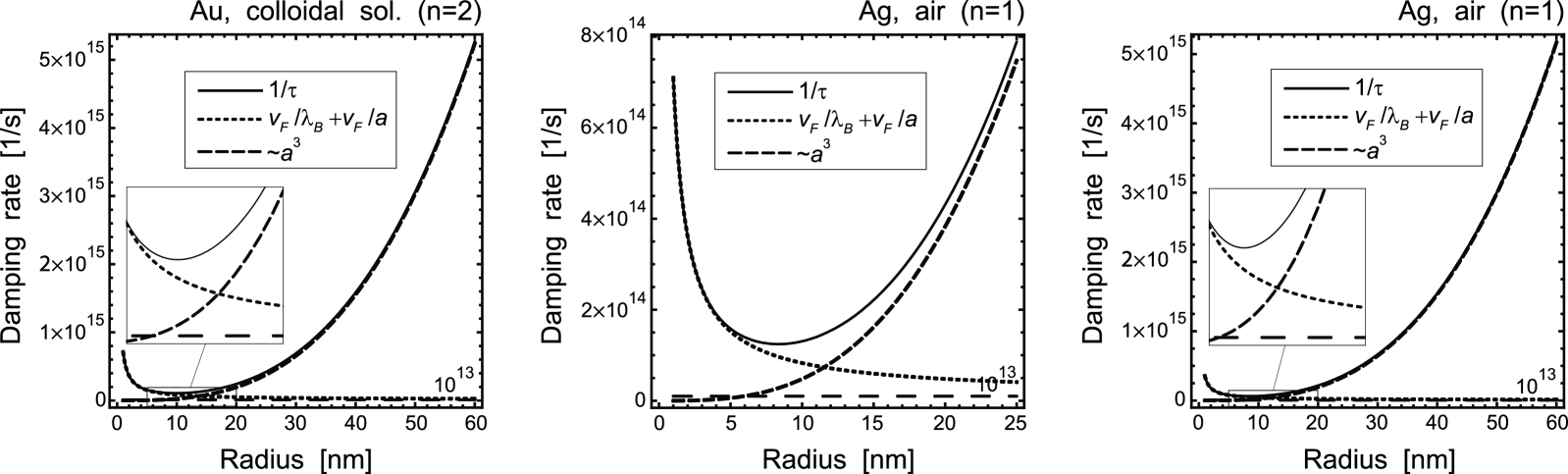
There are various mechanisms of energy dissipation of plasmon oscillations in metallic nanospheres. Let us concentrate on damping of surface plasmons described by . The interaction with phonons, electrons and lattice defects contribute to the relaxation rate with the , which is determined by the mean free path of electrons in the nanosphere, reduced additionally in comparison to the bulk case by inelastic scatterings with the sphere surface. One can use the estimationatwater , where —Fermi velocity, —an effective value of the mean free path, —constant of order 1, —nanosphere radius (for Ag, m/s, nm, which for nm gives s-1, while rather a femtosecond decay time agrees with the measurements on Ag nanoparticlesag ). Note that decomposition of surface plasmons due to creation of particle–hole pairs (Landau damping)ekardt1 ; weick1 is efficient only for small clustersweick1 .
Another type of energy dissipation can be associated with the radiation decay. The far-field radiation (i.e. for distances much longer than the wave-length ) gives the contribution to the relaxation s-1 (for s-1) per single electron due to the Lorentz frictionlan . If one multiplies it by the electron number (in order to account for the probability of energy transfer from the total system), one can arrive at the value , which dominates over for not too small spheresksi ; kre ; ag . This channel of plasmon energy dissipation allows for explanation of the surface plasmon oscillations behavior with growing (as scales as ) for nanospheres embedded in a dielectric medium (like in the water—as it is presented in the Tab. 1 for nanoparticles of gold). The more precise derivation of the far-field radiation losses expressed by is presented in Appendix B, leading to the same formula for as given above. Note that if the attenuation rate is closer to 1 then the attenuation induced shift of the self-frequency is greater, and this behavior coincides with experimental observationswzr1 ; wzr2 (for the overdamped regime is attained without free plasmon oscillations).
| Tab. 1. Comparison with experimental datawzr2 for Au nanospheres in water | ||||
| nanosphere radius | 50 nm | 40 nm | 25 nm | |
| attenuation rate due to far-field radiation losses | 1.51 | 2.95 | 12.09 | |
| shifted self-frequency rate | 0.75 | 0.94 | 0.99 | |
| red-shifted oscillation energy | (theor.) | 2.16 eV | 2.70 eV | 2.87 eV |
| red-shifted oscillation energy | (exper.) | 2.16 eV | 2.26 eV | 2.36 eV |
For Au, eV, and surface plasmon energy eV. This value of is estimated assuming a coincidence of theoretically predicted self-frequency shifted by attenuation with experimentally measured for nm; note that the discrepancy between the experimental red-shift and the theoretical one grows for smaller , which is probably caused by the strengthening of an impact of at smaller , resulting in decrease of the red-shift in comparison to its value caused by . This tendency at decreasing radius seems to be confirmed also by measurements for silver clusters with small dimensions nm, which was reported in Refs stietz, ; scharte, .
Note that for small metallic clusters, quantum spill-out of electron cloud beyond positive jellium causes a red-shift of resonance Mie frequency lowering, however, with radius growth (thus it is in fact a blue-shift with radius growth). The additional effect of polarization of ionic system (this effect is beyond jellium model) can lead oppositely to inverse frequency shift, though rather small. Some jellium oscillation corrections can be also accounted for as scattering with phonons and can be included in the effective time rate for damping via effective mean free path . The corresponding contributions are, however, significant rather for small systems brack ; ekardt (for summarizing of various effects caused red and blue shifts of resonance with radius growth, cf. also Ref. kreib, ). We consider the range of sphere dimensions when radiation losses cause overwhelming contribution to damping and to the resulting red-shift of the surface plasmon resonance, cf. Fig. 1. In this figure it is presented comparison of damping contributions due to scattering effects, and due to radiation losses in dielectric surroundings, . For nm the latter channel clearly dominates. The radiation-caused red-shift grows strongly with the radius of the nanosphere similarly as it is observed in the experiment for range of sphere radii 25–50 nm (for Au) wzr2 .
The next source of the attenuation of surface plasmons would be connected with the transport of dipole oscillation energy between nanoparticles due to the Förster-type couplingatwater in the case of sufficiently dense location of metallic nanoparticles. Nevertheless, taking into account that for uniform nanoparticle distribution in the dielectric medium, the same energy rates simultaneously escape and arrive at particular nanosphere due to interaction with other nanospheres (nearest-neighbors), this coupling does not contribute to the relaxation time (at least for uniformly distributed metallic nanocomponents).
The situation changes, however, significantly if metallic nanoparticles are deposited on the surface of the semiconductor substrate. Then the near-field e-m energy transfer from oscillating dipoles (surface plasmons with ) to the electrons in substrate semiconductor starts to be the dominant channel of surface plasmon dissipation. One can estimate the corresponding time-rate by the Fermi golden rule applied to the system of plasmons coupled in near-field zone with semiconductor substrate. One can consider two situations, the first one—with rapidly switched off external electric field, which excites surface plasmons, then gradually (with lowering amplitude of oscillations) transferring energy to the semiconductor, and the second one—a stationary state of plasmons (with constant amplitude) with mediating role of plasmons transferring entire energy of incident photons to semiconductor. The latter case corresponds thus to a stationary solution of a driven and damped oscillator, while the former one to free damped oscillations. In both cases the damping rate is the same, as it corresponds to the same substrate in a near-field zone. For free damped oscillations the total initial oscillation energy (assessed in Appendix B) is gradually lost with the time ratio . It allows for calculation of the , which is presented in the Appendix C. Utilizing the similar calculus as in Appendix B one can assess the value of the corresponding damping rate , assuming that the total energy loss of surface plasmons is transferred to the semiconductor substrate with additional renormalization by a factor lowering an efficiency of this channel ( is a phenomenological factor introduced in order to account for geometry-induced proximity type constraints imposed on the dipole near-field coupling of the nanosphere with underlying semiconductor layer). Thus it is sufficient to calculate the energy income in the semiconductor due to nanosphere near-field dipole coupling—as it is done in Appendix C (within the Fermi golden rule scheme). For this channel of surface plasmon energy dissipation we deal with the scaling of the resonance energy shift with the dot radius, similar as that for , however, with possible correction induced by dependence on (it may be important, as for the nanosphere located on the planar semiconductor surface one can use an estimation , [for nm] where is a constant, is an effective range of near-field coupling). The parameter significantly grows in the case when the total nanosphere is in the near-field contact with the substrate, i.e. when the nanosphere is completely embedded in the semiconductor medium. For nanospheres deposited on the real semiconductor surface, the parameter is obtained through fitting the experimental data (cf. Tab. 2).
Assuming stationary conditions (i.e., constant in time amplitude of the surface plasmon oscillations, which corresponds to a balance of the incoming energy of incident photons with the energy outgoing to semiconductor substrate) the relevant damping is governed by the near-field dipole interaction (for ) expressed by the scalar potentiallan with an amplitude ,
| (27) |
The matrix element of near-field dipole interaction for the transition of a semiconductor electron from the state in the valence to the conduction band, assumed as (–initial, –final, respectively) is calculated in Appendix C, (Eq. (60)), which leads to a probability of transition per time unit, , where is the surface plasmon dipole oscillation amplitude, adjusted to the balance of energy income and outcome (via shift of the resonance for stationary driven and damped oscillations).
Taking into account that the number of incident photons in the volume of semiconductor equals and the volume rate of metallic components (—the number of nanospheres), the probability that an energy of a single incident photon is transferred to the semiconductor via surface plasmons on metallic nano-admixtures can be expressed as (with given by Eq. (60)):
| (28) |
where is the amplitude of forced surface plasmon oscillations.
In order to assess an efficiency of the near-field coupling channel one can estimate the ratio of probability of energy absorption in semiconductor via mediation of surface plasmons (per single photon incident on the metallic nanospheres) to the energy attenuation in semiconductor directly from a planar wave illumination (also per single photon). In the latter case the energy attenuation in the semiconductor per single incident photon is given by the formula for ordinary photo-effect, (cf. e.g., Ref. pol, ). The ratio turns out to be of order of (at a typical surface density of nanoparticles, /cm2) which (including the phenomenological factor and —semiconductor photo-active layer depth) is sufficient to explain the scale of experimentally observed strong enhancement of absorption and emission rates. It should be noticed that grows with (cf. Eq. (64)) and would attain the critical value for overdamped oscillator (), which precludes surface plasmon free oscillations.
Very high efficiency (even if diminished by ) of the near-field energy transfer from surface plasmons to semiconductor substrate is caused mainly by a contribution of all interband transitions, not restricted here to the direct (vertical) ones as for ordinary photo-effect, due to absence of the momentum conservation constraints for nanosystems—cf. Appendix C. The strengthening of the probability transition due to all indirect interband paths of excitations in semiconductor is probably responsible for observed experimentally strong enhancement of light absorption and emission in diode systems mediated by surface plasmons in nanoparticle surface coveringswzmocn1 ; wzmocn2 ; wzr1 ; wzr2 ; wzr3 ; wzr4 .
In the balanced state of the system when the incoming energy of light is transferred to the semiconductor via near-field coupling, we deal with the stationary solution of driven and damped oscillator. The driving force is the electric field of the incident planar wave, the damping force is the near-field energy transfer described by the (assuming that this dissipation channel is dominating). The resulting red-shifted resonance with simultaneously reduced amplitude allows for the accommodation to the balance of energy transfer to semiconductor with incident photon energy. The amplitude of resonant plasmon oscillations is thus shaped by . The extremum of red-shifted resonance is attained at with corresponding amplitude . This shift is proportional to and scales with nanosphere radius similarly (diminishes with decreasing ) as in the experimental observationswzr2 (note again that for the dependence on is opposite [grows with decreasing ]).
In order to compare with the experiment let us estimate the photo-current in the case of metallically modified surface in relation to the ordinary photo-effect. The photo-current is given by , where is the number of incident photons, and are probabilities of single photon attenuation in ordinary photo-effectpol and due to presence of metallic nanospheres, i.e., of (cf. Ref. pol, ) and given by Eq. (28); is the amplification factor ( the annihilation time of both sign carriers, the drive time for carriers [the time of traversing the distance between electrodes]). From the above formulae it follows that (here , i.e., the photo-current without metallic modifications),
| (29) |
where , with the surface density of metallic nanospheres, the semiconductor layer depth, , , , , eV, is the effective mass of conduction band and valence band carriers (for , and , for light (heavy) carriers, band gap eV, ), is the bare electron mass.
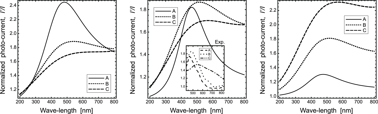
The results are summarized in Tab. 2 and in Fig. 2, for various radii of the nanospheres, and reproduce well the experimental behavior reported in Ref.wzr2, . By we denote frequencies corresponding to maximum value of the photo-current (i.e., to maximum of ).
| Tab. 2. Comparison with the experimental datawzr2 for Au nanospheres on Si layer | ||||||
| [nm] | [108/cm2] | (theor) [eV] | (exp) [eV] | |||
| 50 | 0.8 | 0.772 | 2.09 | 2.25 | 0.84 | 1.55 |
| 40 | 1.6 | 0.951 | 2.58 | 2.48 | 3.00 | 1.9 |
| 25 | 6.6 | 0.997 | 2.71 | 2.70 | 49.42 | 1.75 |
(the best coincidence with the experimental data is attained at )
In Fig. 2 an estimation of normalized photo-current, , with respect to wave-length is presented, for three sizes of metallic nanospheres (Au) deposited on photo-active Si layer, with structure parameters as listed below (the proximity parameter ):
| Legend to Fig. 2 | |||
|---|---|---|---|
| panel in Fig. 2 | radius [nm] | concentration [] | layer depth [m] |
| left | (A) 25, (B) 40, (C) 50 | (A) 6.6, (B) 1.6, (C) 0.8 | 2 |
| central | (A) 19, (B) 40, (C) 50 | (A) 6.6, (B) 1.6, (C) 0.8 | 230 |
| right | (A) 25, (B) 40, (C) 50 | (A) 1.5, (B) 1.5, (C) 1.5 | 230 |
As it was indicated above, the relatively high value of makes possible a significant growth of efficiency of the photo-energy transfer to semiconductor, mediated by surface plasmons in nanoparticles deposited on the active layer, by increasing or reducing (at constant ). However, because of the fact that an enhancement of easily induces the overdamped regime—cf. Eq. (64), a more perspective would be thus lowering of , the layer depth (cf. Fig.2 (left), where a significant growth of photo-current with lowering of active layer depth illustrates the surface character of the effect). The overall behavior of calculated according to the relation (29), and depicted in the central panel in Fig. 2, agrees quite well with the experimental observations presented in Fig. 4 of Ref. wzr2, (cf. inset in the central panel of Fig. 2), both in position, height and shape of photo-current curves for distinct samples (the strongest enhancement is achieved for nm at densities as indicated above, in the Legend to Fig. 2), though is probably overestimated as the denominator would be greater for doped real semiconductor structure which was not taken into account in the present calculus, similarly as surface effects—all of these would change the denominator as well as its energy dependence, especially for longer wavelengths, where the discrepancy between theoretical model and experimental data is noticeable.
IV Comments and conclusions
The presented analysis featuring semiclassical RPA-type approach to collective fluctuations in metallic nanosphere in ’jellium’ model deals with two types of plasmons, surface and volume ones. Within this approximation the self-frequencies of surface plasmon modes are independent of the sphere radius (similarly as classical Mie frequency for dipole surface oscillations). There are, however, also surface modes induced by the volume modes and frequencies of these volume-induced surface oscillations depend on the sphere radius, similarly as the self-frequencies of the volume plasmons (given by the dispersion relation , —nodes of the th spherical Bessel function). The e-m response of the sphere consists of both resonance types, the surface and the volume ones. It should be, however, emphasized that exciting of the volume modes is limited by the nanoscale of the system resulting in almost uniform e-m wave fields for resonant wavelength (dipole approximation regime). The uniform over the sphere, dynamic electric field excites the surface plasmons but not the radius-dependent volume modes. Therefore one can conclude that the experimentally observed significant dependence of resonant e-m frequencies on the radius of nanoparticleswzr2 should be addressed to more complicated phenomena than radius dependent volume modes.
The shift of the resonance frequency (in particular of Mie dipole type oscillations) for small clusters (up to nm) was analyzed against various quantum effects in microscopic type approaches, mainly of TDLDA typebrack ; ekardt ; weick also within semiclassical approacheskresin . All these investigations indicate a major component of the experimentally observed red-shift of Mie frequency due to quantum spill-out effect (via reducing of density of electrons, resulting in factor for resonance frequency, where the spill-out volume , i.e., number of electrons outside the jellium edge, was the subject of various microscopic estimationsbrack ; kresin ; ekardt ; weick ). Described in that manner red-shift of the resonance turns out, however, insufficient in comparison to experimental datakresin ; ekardt ; weick1 . It is lower than observed in the experiment for ultra-small clustersbrack ; kresin . The contribution to red-shift, also important rather in small clusters, was obtained due to decay of plasmons for particle-hole pairs (Landau damping)ekardt1 ; weick1 , which improved fitting with the experiment. Additionally it was predicted an opposite blue-shift due to multi-plasmon anharmonic contributiongerch . For larger cluster it was indicated that the dominating spill-out factor weakens as brack ; kresin ; ekardt ; weick and for considered in the present paper region of nanosphere dimensions (above 10 nm up to 60 nm) is negligible in comparison to predominant in this region of nanosphere radii radiation loss contribution (cf. also Fig 1).
Note. that within microscopic approach TDLDA more difficult it is to explain microscopically the observed width of resonance peak than its positionbrack . The processes which would contribute are: spontaneous ionization, Landau damping (i.e., interference of collective state with particle-hole pair with similar energy), evaporation of ion, ion vibrations (above jellium model). For larger , above 10 nm, the dominating contribution to peak widthkreib is caused by irradiation effects which are stronger than scattering contribution (and C—constant of order 1 and —effective mean path, were estimated by many authors, cited in Ref. brack, , in particular including Landau damping type fragmentation of collective excitation).
The quantum spill-out, Landau damping and coupling to ion excitations (beyond jellium model), though important for small clusters, are thus rather weak for large nanospheres and contribute resonance shift for radius range above 10 nm far lower than experimentally observed. Another possibility for radius dependence of resonant frequencies is connected with the interaction of surface plasmons with other components of the system, which leads to damping of these oscillations. A shift of the resonance for driven and damped oscillator depends on the attenuation rate, which scales with the nanosphere radius. We have analyzed various channels of surface plasmon damping. The most effective channel for the surface plasmon damping is connected with the dipole-type near-field coupling of the surface dipole plasmons with semiconductor substrate, on which metallic nanospheres would be deposited, e.g., in nanomodified diode-type systems. Due to nano scale of the spheres for this coupling the momentum is not conserved, which results in a strong enhancement of the interband transition probability (because all indirect electron transitions between valence and conductivity bands in substratum have to be accounted for, provided energy conservation alone). It agrees with the experimental data referred to a significant growth of the energy transfer from surface plasmons in metallic nanoparticles to substrate semiconductor.
In order to include the damping of surface plasmons one can introduce a phenomenological damping factor (attenuation time) to the oscillation semiclassical RPA equation for electron local density fluctuations. As the form of the resulting equation is of the damped oscillator type, thus attenuation causes the red shift in the resonance frequency, . For driven and damped stationary oscillations, the red-shift of a resonance takes place with maximal amplitude at . This red-shift is dependent on the sphere radius, via radius-dependence of .
Energy transfer to semiconductor surroundings mediated by surface plasmons is so effective that it may easily cause overdamped regime for plasmon oscillations. This channel is, however, reduced (typically by three orders in magnitude) by proximity constraints. Nevertheless, for nanospheres deposited on the semiconductor surface even only small fraction of the near-field channel (, for nm, is an effective range of the near-field coupling) causes a strong damping of plasmons. If to embed the nanospheres in semiconductor medium the plasmon system would fall in the overdamped regime ().
In the case of a small contact of the metallic nanospheres with the semiconductor substrate or in the case of an absence of semiconductor surroundings, a significant contribution to plasmon attenuation is due to far-field radiation and electron scattering effects. The radiation contributions to scale with particle radius as (for both far- and near-field channels, though in the latter case the proximity constraints, included in , would modify this dependence to the linear one), while for scattering contribution, . Thus the total attenuation rate ( constants). For relatively big spheres ( nm) the radiation channels prevail, while for smaller ones the scatterings would be also importantstietz ; scharte .
The reported strengthening of photo-voltaic effects due to plasmonic concentrators (layer of metallic nanoparticles on active semiconductor surface with of order of /cm2), for instance: up to 20-fold increase of photo-current in Si with nanoparticles Ag (40 nm [2-fold increase], 66 nm [8-fold], 108 nm [20-fold])wzr1 , indicate the significant role of near-field energy transfer growing with the sphere radius. Another observations confirm also the strengthening role of plasmonic oscillations for emission and absorption phenomena in semiconductor diode systems, e.g., 9-fold increase of emission from Si diode modified with nanoparticles Ag of elliptical shape 120x60 nm, and resonant emission shift after covering nanoparticles Ag with 30 nm layer of ZnSwzr4 ; wzr5 and up to 14-fold increase of absorption with various metal nanoparticles: Ag (12 nm [3-fold], Au (10 nm [5-fold], Cu (10 nm [14-fold])wzr3 . Influence of dielectric coating is caused by the surface self-oscillation sensitivity to dielectric surroundings (as for metallic nanosphere embedded in a dielectric medium), , and for typical it gives strong decrease of resonant frequencies by factor . The best correspondence with the experiment is attained for reported strong dependence of extinction features with respect to nanoparticle size (located on the surface of Si), the shift of the resonant peak corresponding to the change of Au nanoparticles radius: 25–50 nm (stronger extremum for 40 nm)wzr2 and simultaneous enhancement of photo-current seem to be well described by our model.
Some experimental data indicate, however, existence of competitive mechanisms. For instance, for active medium TiO2 the photo-current diminishes in a wide spectral region (excluding the UV range) for coverings with nanoparticles Ag (3–6 nm), while the same coverings on optically active organic medium (DSC—dye solar cell) lead to strong increase of the photo-current for 3 nm Ag, but to the decrease of photo-current for 6 nm Agwzr4 . The competitive factors can be linked here with retardation of the carriers transfer, despite plasmonic strengthening, or with the destructive modification of a photo-sensitive substrate material, for too small nanoparticles (more convenient are probably greater nanoparticleswzr1 ).
Summarizing, in the presented model nanosphere surface plasmons couple with substrate charges (band electrons in a substrate semiconductor) via photon-less short range e-m dipole interaction with very quick timing (thus very effective)—as confirmed by time-resolved spectroscopy measurementswzr2 . The strong enhancement of the efficiency results from nanoscale-induced incommensurability leading to all indirect in momentum interband transitions, not allowed for interaction of band electrons with the original incident planar wave photons as in an ordinary photo-effect. The type of dipole coupling is connected here with a specific e-m field gauge in the vicinity of the nanosphere within the distance lower than the wave-length (thus ’inside’ the single photon), crucially distinct than for the planar wave (in the latter case only vector potential can be used, which is impossible in the former case)lan . The schematically described above scenario qualitatively fits with the experimentally observed behavior and elucidates the timing of the particular steps of the energy-transfer-processes including mediating role of metallic nanosphere surface plasmons. The relevant time rates can be estimated within standard quantum mechanical attitude of Fermi-golden-rule type. Thus the presented above RPA plasmon description supply the convenient and simple tool for further modeling and optimization of the metallically nanomodified solar cell structures, towards enhancement of their efficiency.
Acknowledgements.
Supported by the Polish KBN Project No: N N202 260734 and the FNP Fellowship START (W. J.).Appendix A Analytical solution of plasmon equations for the nanosphere
Below we present a method of solution of Eqs (15, 16). For the solution of Eq. (15) we assume in accordance with the rotational symmetry: (with an initial condition ). After substituting it into Eq. (15) we obtain:
| (30) |
The function (nonsingular at ) has thus the form:
| (31) |
where –const., (–inverse Thomas-Fermi radius), (bulk plasmon frequency). For we assume a single harmonics , as for a linear differential equation and suitably to the initial condition. Thus from Eq. (30) we obtain:
| (32) |
with . A solution nonsingular at has the form:
| (33) |
where –constant, –the spherical Bessel function [–the Bessel function of the first order], –the spherical function (–the spherical angle). Owing to the quasiclassical boundary condition, , one has to demand , which leads to the discrete values of , (where , are nodes of ), and next to the discretization of self-frequencies :
| (34) |
The general solution for has thus the form
| (35) |
The neutrality condition, , with , can be rewritten as follows: , , . Taking into account also the continuity condition on the spherical particle surface, , one can obtain: and it is possible to fit (cf. Eq. (31)) and constants: , . From the condition and Eq. (35) it follows that , (because of ). Therefore the internal-volume electron fluctuations in the sphere have the form:
| (36) |
Now let us solve the Eq. (16) for surface electron fluctuations assuming . In order to remove the Dirac delta functions we integrate both sides of the Eq. (16) with respect to the radius length () and then we take a limit to the sphere surface, . It results in the following equation:
| (37) |
Note that the last term in the above equation describes a coupling between volume and surface plasmon excitations. The two first terms of the right-hand-side of the Eq. (37) vanish in the limit due to the delta function properties, and the third term gives the contribution: . The fourth and fifth terms contribute in the following manner:
| (38) |
In the derivation of the fourth term we have used (for ):
| (39) |
where is the Legendre polynomial [], is an angle between vectors and , while in the derivation of the fifth term ():
| (40) |
In the derivation of the last term in the Eq. (38) we used the explicit forms of and , together with the neutrality condition, . The above described procedure leads to the equation for the surface plasmons:
| (41) |
where . Taking into account the spherical symmetry, one can assume the solution of the above equation in the form:
| (42) |
After substituting it into the Eq. (41) we find:
| (43) |
The solutions of the above pair of equations have the form:
| (44) |
And finally,
| (45) |
Additionally let us comment on the equation for the case of nanosphere embedded in the dielectric medium with —cf. Eq. (25). The solutions of this equations are the same as presented above, however, with the frequencies modified as follows: .
Appendix B Calculation of time rate for far-field dipole-type radiation of nanosphere surface plasmons
In order to estimate the attenuation coefficient due to far-field radiation losses one can consider damping of nanosphere plasmons rapidly excited by switching off the uniform electric field, . The corresponding oscillations of the local electron density can be described by the equations:
| (46) |
for , and
| (47) |
for (). For not dependent on , the driving force enters to the second equation only and leads to the driven solution corresponding to the dipole surface plasmon oscillations . Similarly, one can conclude that for nanospheres the visible light does not excite nanosphere volume plasmons as within the dipole approximation the incident wave electric field is uniform all over the sphere, unless the dipole approximation does not hold (i.e., when ).
For (the rapid switching off the constant electric field ) the solution of Eq. (47) has the form:
| (48) |
where and is undamped dipole self-frequency.
It is easy to calculate the loss of the total energy of the system , i.e., by taking into account both kinetic and potential energy of electron system. Only potential interaction energy of oscillating electrons contributes, and , [the time dependent part of energy is caused by interaction of excited electrons, , with , ]. For given Eq. (48) one can find,
| (49) |
since .
On the other hand, assuming that damping of oscillations is caused by far-field radiation, one can calculate the energy loss using the Poynting vector , with . The scalar potential of the e-m wave emitted by the surface plasmon dipole oscillations: is of the retarded form, , and for , , here and the dipole moment . In our case of surface plasmon dipole oscillations
| (50) |
Similarly, for the retarded vector potential we find , [because of , for the sphere and due to , which gives ].
Hence, for far-field radiation of surface plasmon dipole oscillations we have
| (51) |
and
| (52) |
which corresponds to the planar wave, and , ( is the angle between and ). Next, taking into account that , one can find . For as in Eq. (50), with given by Eq. (48), one can find in this manner,
| (53) |
The latter integral equals to , which together with, , leads to the expression:
| (54) |
Via a comparison with Eq. (49), we finally find,
| (55) |
Appendix C Calculation of damping time rate due to near-field interaction of surface plasmons with semiconductor substrate
For the near-field regime () the vector potential has the same form as previously for far-field since only condition was used for its derivationlan , . In the near-field region the e-m field is not of planar wave type and both vector and scalar potentials are needed to describe it. The scalar potential attains the form , (due to the Lorentz gauge conditionlan , ). The resulting Fourier components of fields and (i.e. for monochromatic can be thus represented in this case aslan :
| (56) |
and
| (57) |
where we use the notation for the retarded argument, . For near-field region one can neglect terms with and . Assuming also that for near-field one can obtain thus and , which corresponds to dipole electric field.
The dipole type near-field potential can be written as follows:
| (58) |
where ; one can confine Eq. (58) only to the term corresponding to energy absorption in the semiconductor. Then, according to the Fermi golden rule, the transition probability per time unit between states (semiconductor electron states from the valence and conduction bands, respectively), equals
| (59) |
where . Taking axis along the vector , then , ( is an angle between and ). Hence, , [as ], and probability of transition . In order to include all possible initial and final states in semiconductor, the summation with respect to and has to be performed (including filling factors and , as well as absorption and emission of energy). In the result we arrive with the total transition probability in semiconductor per time unit caused by dipole surface plasmon oscillations on the single nanosphere.
Let us emphasize that due to absence of the momentum conservation for the near-field dipole coupling in a vicinity of the nanosphere all interband transitions contribute, not only direct ones as for the interaction with the planar wave. It results in strong enhancement of the transition probability for the near-field coupling in comparison to photon (planar waves) attenuation rate in a semiconductor in an ordinary photo-effect.
For the simplest model band structure, , where , and ( is the semiconductor band gap) the integration over wave vectors gives the formula for the total probability of the transition
| (60) |
where .
Assuming now that the dipole plasmon oscillations correspond to the damped oscillations which were excited by the rapid switching off the uniform electric field (as in the Appendix B), , with the dipole-type solution for electron distribution given by Eq. (48), we have
| (61) |
with
| (62) |
in comparison to the Eq. (48) we have neglected here the second term for well greater than unity.
One can now estimate the total energy transfer to the semiconductor (assuming that the dominant channel of the dissipation is the near-field interaction with semiconductor substrate and neglecting here the small shift of due to dissipation)
| (63) |
where accounts for the proximity constraints which reduce the near-field contact of the sphere with the semiconductor medium; for the case of nanospheres deposited on the semiconductor layer surface , for nm ( is an effective range of the near-field coupling), for the nanospheres entirely embedded in semiconductor surroundings would enhance significantly. Comparing the value given by the formula (63) with the energy loss given by Eq. (49) one can find
| (64) |
For nanospheres of Au deposited on Si layer we obtain:
| (65) |
for light(heavy) carriers in Si, , , and eV, , eV.
References
- (1) W. L. Barnes, A. Dereux, and T. W. Ebbesen, Nature 424, 824 (2003)
- (2) A.V. Zayats, I. I. Smolyaninov, and A. A. Maradudin, Phys. Rep. 408, 131 (2005)
- (3) S.A. Maier, Plasmonics: Fundamentals and Applications (Springer, Berlin 2007)
- (4) S. Pillai, et al., Appl. Phys. Lett. 88, 161102 (2006)
- (5) M. Westphalen, U. Kreibig, J. Rostalski, H. Lüth, and D. Meissner, Sol. Energy Mater. Sol. Cells 61, 97 (2000), M. Gratzel, J. Photochem. Photobiol. C: Photochem. Rev. 4, 145 (2003)
- (6) H. R. Stuart and D. G. Hall, Appl. Phys. Lett. 73, 3815 (1998); H. R. Stuart and D. G. Hall, Phys. Rev. Lett. 80, 5663 (1998); H. R. Stuart and D. G. Hall, Appl. Phys. Lett. 69, 2327 (1996)
- (7) D. M. Schaadt, B. Feng, and E. T. Yu, Appl. Phys. Lett. 86, 063106 (2005)
- (8) K. Okamoto, et al., Nature Mat. 3, 601 (2004); K. Okamoto, et al., Appl. Phys. Lett. 87, 071102 (2005)
- (9) C. Wen, K. Ishikawa, M. Kishima, K. Yamada, Sol. Cells 61, 339 (2000)
- (10) P. Lalanne, J. P. Hugonin, Nature Phys. 2, 551 (2006)
- (11) G. Mie, Ann. Phys. 25, 329 (1908)
- (12) M. B. Mohamed, V. V. Volkov, S. Link, and M. A. El-Sayed, Chem. Phys. Lett. 317, 517 (2000)
- (13) G. T. Boyd, Z. H. Yu, and Y. R. Shen, Phys. Rev. B 33, 7923 (1986)
- (14) E. Hao, R. C. Bayley, G. C. Schatz, J. T. Hupp, and S. Li, Nano Lett. 4, 327 (2004)
- (15) C. Burda, X. Chen, R. Narayanan, M. A. El-Sayed, Chem. Rev. 105, 1025 (2005)
- (16) M. Brack, Rev. of Mod. Phys. 65, 677 (1993)
- (17) V. V. Kresin, Phys. Rep. 220, 1 (1992)
- (18) W. Ekardt, Phys. Rev B 31, 6360 (1985)
- (19) W. Ekardt, Phys. Rev. B 33, 8803 (1986)
- (20) G. Weick, R. A. Molina, D. Weinmann, and R. A. Jalabert, Phys. Rev. B 72, 115410 (2005)
- (21) G. Weick, G. L. Ingold, R. A. Jalabert, and D. Weinmann, Phys. Rev. B 74, 165421 (2006)
- (22) L. Serra, F. Garcias, M. Barranco, N. Barberan, and J. Navarro, Phys. Rev. B 41, 3434 (1990)
- (23) A. Rubio and L. Serra, Phys. Rev. B 48, 18222 (1993)
- (24) L. G. Gerchikov, C. Guet, and A. N. Ipatov, Phys. Rev. A 66, 053202 (2002)
- (25) M. Brack, Phys. Rev. B 39, 3533 (1989)
- (26) W. Ekardt, Phys. Rev. Lett. 52, 1925 (1984)
- (27) C. F. Bohren, D. R. Huffman, Absorption and Scattering of Light by Small Particles (Wiley, New York, 1983)
- (28) U. Kreibig, M. Vollmer, Optical Properties of Metal Clusters (Springer, Berlin, 1995)
- (29) A. B. Migdal, J. Phys. USSR 8, 331 (1944)
- (30) H. von Steinwedel and J. H. D. Jensen, Z. Naturforsh. A 5, 413 (1950)
- (31) M. Goldhaber and E. Teller, Phys. Rev. 74, 1046 (1948)
- (32) D. Pines, Elementary Excitations in Solids (ABP Perseus Books, Massachusetts, 1999)
- (33) D. Pines and D. Bohm, Phys. Rev. 85, 338 (1952); D. Bohm and D. Pines, Phys. Rev. 92, 609 (1953)
- (34) J. I. Petrov, Physics of Small Particles (Nauka, Moscow, 1984)
- (35) B. Lamprecht, A. Leitner, and F. R. Aussenegg, Appl. Phys. B: Lasers Opt. 64, 269 (1997)
- (36) M. L. Brongersma, J. W. Hartman, and H. A. Atwater, Phys. Rev. B 62, R16356 (2000)
- (37) L. D. Landau and E. M. Lifshitz, Field Theory (Nauka, Moscow, 1973)
- (38) F. Stietz et al, Phys. Rev. Lett. 84, 5644 (2000)
- (39) M. Scharte et all., Appl. Phys. B: Laser Opt. 73, 305 (2001)
- (40) U. Kreibig and L. Genzel, Surf. Sci. c156, 678 (1985)
- (41) P. S. Kiriejew, Physics of Semiconductors (PWN, Warsaw, 1969)