Implementation of Nano-scale Rectifiers: An Exact Study
Abstract
We propose the possibilities of designing nano-scale rectifiers using mesoscopic rings. A single mesoscopic ring is used for half-wave rectification, while full-wave rectification is achieved using two such rings and in both cases each ring is threaded by a time varying magnetic flux which plays a central role in the rectification action. Within a tight-binding framework, all the calculations are done based on the Green’s function formalism. We present numerical results for the two-terminal conductance and current which support the general features of half-wave and full-wave rectifications. The analysis may be helpful in fabricating mesoscopic or nano-scale rectifiers.
pacs:
73.63.-b, 73.63.Rt, 81.07.NbI Introduction
Low-dimensional model quantum systems have been the objects of intense research in theory as well as in experiment since these simple looking systems are prospective candidates for future generation of nano-devices in electronic engineering. Several striking features are exhibited by these systems owing to the quantum interference effect which is generally preserved throughout the sample only for much smaller sizes, while the effect disappears for larger systems. A normal metal mesoscopic ring is a very nice example where the electronic motion is confined and the transport becomes coherent. Current trend of miniaturization of electronic devices has resulted much interest in characterization of ring type nanostructures. There are several methods for preparation of such rings. For example, gold rings can be designed by using templates of suitable structure in combination with metal deposition via ion beam etching hobb ; pearson . More recently, Yan et al. have prepared gold rings by selective wetting of porous templates using polymer membranes yan . Using such rings we can design nano-scale rectifiers and to reveal this fact the ring is coupled to two electrodes, to form an electrode-ring-electrode bridge, where AC signal is applied. Electron transport through a bridge system was first studied theoretically by Aviram and Ratner aviram in . Following this pioneering work, several experiments have been done through different bridge systems to reveal the actual mechanism of electron transport. Though, to date a lot of theoretical mag ; lau ; baer1 ; baer2 ; baer3 ; tagami ; gold ; cui ; orella1 ; orella2 ; fowler ; peeters as well as experimental works reed1 ; reed2 ; tali ; fish on two-terminal electron transport have been done addressing several important issues, yet the complete knowledge of conduction mechanism in nano-scale systems is still unclear to us. Transport properties are characterized by several significant factors like quantization of energy levels, quantum interference of electronic waves associated with the geometry of bridging system adopts within the junction, etc. Electronic transport through a mesoscopic ring is highly sensitive on ring-to-electrode interface geometry. Changing the interface structure, transmission probability of an electron across the ring can be controlled efficiently. Furthermore, electron transport in the ring can also be modulated in other way by tuning the magnetic flux, the so-called Aharonov-Bohm (AB) flux, penetrated by the ring. The AB flux can change the phases of electronic wave functions propagating through different arms of the ring leading to constructive or destructive interferences, and accordingly, the transmission amplitude changes.
In the present work we illustrate the possibilities of designing nano-scale rectifiers using mesoscopic rings. To design a half-wave rectifier we use a single mesoscopic ring, while two such rings are considered for designing a full-wave rectifier. Both for the cases of half-wave and full-wave rectifiers, each ring is threaded by a time varying magnetic flux which plays the central role for the rectification action. Within a tight-binding framework, a simple parametric approach muj1 ; san3 ; muj2 ; san1 ; sam ; san2 ; hjo ; walc1 ; walc2 is given and all the calculations are done through single particle Green’s function technique to reveal the electron transport. Here we present numerical results for the two-terminal conductance and current which clearly describe the conventional features of half-wave and full-wave rectifications. Our exact analysis may be helpful for designing mesoscopic or nano-scale rectifiers. To the best of our knowledge the rectification action using such simple mesoscopic rings has not been addressed earlier in the literature.
The paper is organized as follows. With the brief introduction (Section I), in Section II, we describe the model and the theoretical formulations for our calculations. Section III presents the significant results, and finally, we conclude our results in Section IV.
II Model and synopsis of the theoretical background
II.1 Circuit configuration of a half-wave rectifier
We begin by referring to Fig. 1. A mesoscopic ring, threaded by a time varying magnetic flux , is attached symmetrically to two semi-infinite one-dimensional (D) metallic electrodes, namely, source and drain. Two end points C and D of secondary winding of the transformer
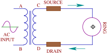
are directly coupled to the source and drain, respectively, through which AC signal is applied. Mathematically, we can express the AC signal in the form,
| (1) |
where, is the peak voltage, corresponds to the angular frequency and represents the time. For the rectification action, we
choose the flux passing through the ring in the square wave form as a function of time. Mathematically it can be written as,
| (2) | |||||
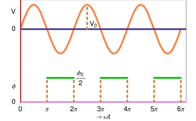
where, () is the elementary flux-quantum. Both the AC signal and threaded magnetic flux vary periodically with the same frequency . The variations of AC input signal (orange line) and magnetic flux (green line) are represented graphically in Fig. 2. From the spectra it is clear that in the negative half-cycles of the input signal, the ring is penetrated by the flux , which is required for half-wave rectification.
II.2 Circuit configuration of a full-wave rectifier
The circuit diagram for a full-wave rectifier is schematically presented in Fig. 3. Here two mesoscopic rings are used, together with a transformer whose secondary winding is split equally into two and has a
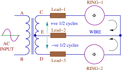
common center tapped connection, described by the point E. The rings are threaded by time varying magnetic fluxes and ,
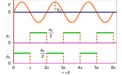
respectively, and their functional forms are described by Eq. 2. A constant phase shift exists between these two fluxes, as schematically shown in Fig. 4, which is essential for full-wave rectification. In the circuit there are three electrodes, namely, lead-1, lead-2 and lead-3, those are directly coupled to the points C, E and D of secondary winding of the transformer, respectively. During positive half-cycle of the AC input signal, lead-1 and lead-2 act as source and drain, respectively. While, for the negative half-cycle of the AC input voltage, lead-3 and lead-2 behave as source and drain, respectively. Thus the circuit consists of two half-wave rectifiers, as shown clearly from Fig. 3. Each rectifier is connected to a single quantum wire through which current flows in one direction during each half-cycle of the AC input signal which is described by the arrows in Fig. 3. The variations of AC input voltage (orange curve) and associated magnetic fluxes (green curves) in the rings are represented graphically in Fig. 4. From the spectra it is observed that, in the positive half-cycles of AC input signal, ring-2 is threaded by the flux . On the other hand, for the negative half-cycles of the input signal, ring-1 is penetrated by the flux .
II.3 Theoretical formulation
Using Landauer conductance formula datta ; marc we determine two-terminal conductance () of the mesoscopic ring. At much low temperatures and bias voltage it () can be written in the form,
| (3) |
where, corresponds to the transmission probability of an electron across the ring. In terms of the Green’s function of the ring and its coupling to two electrodes, the transmission probability can be expressed as datta ; marc ,
| (4) |
where, and describe the coupling of the ring to the source and drain, respectively. Here, and are the retarded and advanced Green’s functions, respectively, of the ring considering the effects of the electrodes. Now, for the full system i.e., the mesoscopic ring, source and drain, the Green’s function is expressed as,
| (5) |
where, is the energy of the source electron. Evaluation of this Green’s function needs the inversion of an infinite matrix, which is really a difficult task, since the full system consists of the finite size ring and two semi-infinite D electrodes. However, the full system can be partitioned into sub-matrices corresponding to the individual sub-systems and the effective Green’s function for the ring can be written in the form marc ; datta ,
| (6) |
where, describes the Hamiltonian of the ring. Within the non-interacting picture, the tight-binding Hamiltonian of the ring can be expressed like,
| (7) |
where, and correspond to the site energy and nearest-neighbor hopping strength, respectively. () is the creation (annihilation) operator of an electron at the site and is the phase factor due to the flux enclosed by the ring consists of atomic sites. A similar kind of tight-binding Hamiltonian is also used, except the phase factor , to describe the electrodes where the Hamiltonian is parametrized by constant on-site potential and nearest-neighbor hopping integral . The hopping integral between the ring and source is , while it is between the ring and drain. In Eq. (6), and are the self-energies due to the coupling of the ring to the source and drain, respectively, where all the information of the coupling are included into these self-energies.
III Numerical results and discussion
To illustrate the results, let us begin our discussion by mentioning the values of different parameters used for our numerical calculations. In the mesoscopic ring, the on-site energy is fixed to for all the atomic sites and nearest-neighbor hopping strength is set to . While, for the side-attached electrodes the on-site energy () and nearest-neighbor hopping strength () are chosen as and , respectively. The hopping strengths and are set as . The equilibrium Fermi energy is taken as .
III.1 Half-wave rectification
The rectification action of the half-wave rectifier is illustrated in Fig. 5. In the upper panel of this figure we plot AC input signal (orange curve) as a function of . The amplitude of the AC signal is fixed at . The variation of conductance (red curve) as a function of is shown in the middle panel. From the results we clearly observe that only in the positive half-cycles of the AC input signal, conductance exhibits finite value. On the other hand, conductance exactly drops to zero for the negative half-cycles of the AC input signal. is the amplitude of the conductance which gets the value , and therefore, the transmission probability goes to unity, according to Landauer conductance formula (see Eq. 3). Now we try to figure out the rectification operation. The probability amplitude of getting an electron from the source to drain across the ring depends on the quantum interference effect of the electronic waves passing through the upper and lower arms of the ring. For a symmetrically connected ring (upper and lower arms are identical to each other), threaded by a magnetic flux , the probability amplitude of getting an electron across the ring becomes exactly zero () for the typical flux, . This vanishing behavior of the transmission probability can be easily obtained through few simple mathematical steps. Therefore, in the negative half cycles of the AC input signal, electron conduction through the ring is no longer possible since the ring encloses the
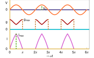
flux for these half-cycles. Only for the positive half-cycles of the AC input signal electron can conduct through the ring as the ring is not penetrated by the flux . This feature clearly describes the half-wave rectification action. To visualize the rectification feature more prominently we present the variation of current (magenta curve) as a function of in the lower panel of Fig. 5. We obtain the current through the ring by integrating over the transmission function (see Eq. 8). Following the conductance pattern (red curve), the vanishing nature of the current in the negative half-cycles of the AC input signal is clearly understood. The non-vanishing behavior (magenta curve) of the current is only achieved for the positive half-cycles of the AC input. All these features clearly support the half-wave rectification action as we get in traditional macroscopic half-wave rectifiers.
III.2 Full-wave rectification
Next, we investigate the behavior of full-wave rectification mechanism as illustrated in Fig. 6. The upper, middle and lower panels correspond to the time varying features of input signal, conductance and current, respectively. Our results demonstrate that both for the positive and negative half-cycles of the input signal non-zero conductance (red curve) is obtained. During the positive half-cycles ring-1 conducts, while for the negative half-cycles conduction takes place through ring-2, as both the two rings enclose time varying magnetic fluxes having identical magnitude with a constant phase shift . The feature of full-wave rectification i.e.,
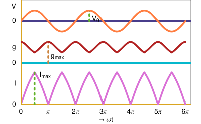
obtaining non-zero conductance for both positive and negative half-cycles of the input signal is attributed to the quantum interference effect as explained earlier in case of half-wave rectification. In the same footing, here we describe the variation of current (magenta curve) with time to support the full-wave rectification operation properly. Here also non-zero value of current is achieved both for the positive and negative half-cycles of the input signal following the conductance spectrum. Our results support the full-wave rectification action and agree well with the basic features obtained in conventional macroscopic full-wave rectifiers.
IV Concluding remarks
In a nutshell, we have proposed the possibilities of designing nano-scale rectifiers using mesoscopic rings enclosing a time varying magnetic flux. The half-wave rectifier is designed using a single mesoscopic rings, while two such rings are used for full-wave rectification. The rectification action is achieved using the central idea of quantum interference effect in presence of flux in ring shaped geometries. We adopt a simple tight-binding framework to illustrate the model and all the calculations are done using single particle Green’s function formalism. Our exact numerical results provide two-terminal conductance and current which support the general features of half-wave and full-wave rectifications. Our analysis can be used in designing tailor made nano-scale rectifiers.
Throughout our work, we have addressed all the essential features of rectification operation considering a ring with total number of atomic sites . In our model calculations, this typical number () is chosen only for the sake of simplicity. Though the results presented here change numerically with the ring size (), but all the basic features remain exactly invariant. To be more specific, it is important to note that, in real situation the experimentally achievable rings have typical diameters within the range - m. In such a small ring, unrealistically very high magnetic fields are required to produce a quantum flux. To overcome this situation, Hod et al. have studied extensively and proposed how to construct nanometer scale devices, based on Aharonov-Bohm interferometry, those can be operated in moderate magnetic fields baer4 ; baer5 ; baer6 ; baer7 .
In the present paper we have done all the calculations by ignoring the effects of the temperature, electron-electron correlation, etc. Due to these factors, any scattering process that appears in the mesoscopic ring would have influence on electronic phases, and, in consequences can disturb the quantum interference effects. Here we have assumed that, in our sample all these effects are too small, and accordingly, we have neglected all these factors in this particular study.
The importance of this article is mainly concerned with (i) the simplicity of the geometry and (ii) the smallness of the size.
References
- (1) K. L. Hobbs, P. R. Larson, G. D. Lian, J. C. Keay, and M. B. Johnson, Nano Lett. 4, 167 (2004).
- (2) D. H. Pearson, R. J. Tonucci, K. M. Bussmann, and E. A. Bolden, Adv. Mater. 11, 769 (1999).
- (3) F. Yan and W. A. Geodel, Nano Lett. 4, 1193 (2004).
- (4) A. Aviram and M. Ratner, Chem. Phys. Lett. 29, 277 (1974).
- (5) M. Magoga and C. Joachim, Phys. Rev. B 59, 16011 (1999).
- (6) J.-P. Launay and C. D. Coudret, in: A. Aviram and M. A. Ratner (Eds.), Molecular Electronics, New York Academy of Sciences, New York, (1998).
- (7) R. Baer and D. Neuhauser, Chem. Phys. 281, 353 (2002).
- (8) R. Baer and D. Neuhauser, J. Am. Chem. Soc. 124, 4200 (2002).
- (9) D. Walter, D. Neuhauser, and R. Baer, Chem. Phys. 299, 139 (2004).
- (10) K. Tagami, L. Wang, and M. Tsukada, Nano Lett. 4, 209 (2004).
- (11) R. H. Goldsmith, M. R. Wasielewski, and M. A. Ratner, J. Phys. Chem. B 110, 20258 (2006).
- (12) W. Y. Cui, S. Z. Wu, G. Jin, X. Zhao, and Y. Q. Ma, Eur. Phys. J. B 59, 47 (2007).
- (13) P. A. Orellana, M. L. Ladron de Guevara, M. Pacheco, and A. Latge, Phys. Rev. B 68, 195321 (2003).
- (14) P. A. Orellana, F. Dominguez-Adame, I. Gomez, and M. L. Ladron de Guevara, Phys. Rev. B 67, 085321 (2003).
- (15) B. T. Pickup and P. W. Fowler, Chem. Phys. Lett. 459, 198 (2008).
- (16) P. Földi, B. Molnar, M. G. Benedict, and F. M. Peeters, Phys. Rev. B 71, 033309 (2005).
- (17) J. Chen, M. A. Reed, A. M. Rawlett, and J. M. Tour, Science 286, 1550 (1999).
- (18) M. A. Reed, C. Zhou, C. J. Muller, T. P. Burgin, and J. M. Tour, Science 278, 252 (1997).
- (19) T. Dadosh, Y. Gordin, R. Krahne, I. Khivrich, D. Mahalu, V. Frydman, J. Sperling, A. Yacoby, and I. Bar-Joseph, Nature 436, 677 (2005).
- (20) C. M. Fischer, M. Burghard, S. Roth, and K. V. Klitzing, Appl. Phys. Lett. 66, 3331 (1995).
- (21) V. Mujica, M. Kemp, and M. A. Ratner, J. Chem. Phys. 101, 6849 (1994).
- (22) S. K. Maiti, Solid State Commun. 149, 1684 (2009).
- (23) V. Mujica, M. Kemp, A. E. Roitberg, and M. A. Ratner, J. Chem. Phys. 104, 7296 (1996).
- (24) S. K. Maiti, Phys. Lett. A 373, 4470 (2009).
- (25) M. P. Samanta, W. Tian, S. Datta, J. I. Henderson, and C. P. Kubiak, Phys. Rev. B 53, R7626 (1996).
- (26) S. K. Maiti, J. Phys. Soc. Jpn. 78, 114602 (2009).
- (27) M. Hjort and S. Staftröm, Phys. Rev. B 62, 5245 (2000).
- (28) K. Walczak, Cent. Eur. J. Chem. 2, 524 (2004).
- (29) K. Walczak, Phys. Stat. Sol. (b) 241, 2555 (2004).
- (30) S. Datta, Electronic transport in mesoscopic systems, Cambridge University Press, Cambridge (1997).
- (31) M. B. Nardelli, Phys. Rev. B 60, 7828 (1999).
- (32) O. Hod, R. Baer, and E. Rabani, J. Phys. Chem. B 108, 14807 (2004).
- (33) O. Hod, R. Baer, and E. Rabani, J. Phys.: Condens. Matter 20, 383201 (2008).
- (34) O. Hod, R. Baer, and E. Rabani, J. Am. Chem. Soc. 127, 1648 (2005).
- (35) O. Hod, E. Rabani, and R. Baer, Acc. Chem. Res. 39, 109 (2006).