Parallel electron-hole bilayer conductivity from electronic interface reconstruction
Abstract
The perovskite SrTiO3-LaAlO3 structure has advanced to a model system to investigate the rich electronic phenomena arising at polar interfaces. Using first principles calculations and transport measurements we demonstrate that an additional SrTiO3 capping layer prevents atomic reconstruction at the LaAlO3 surface and triggers the electronic reconstruction at a significantly lower LaAlO3 film thickness than for the uncapped systems. Combined theoretical and experimental evidence (from magnetotransport and ultraviolet photoelectron spectroscopy) suggests two spatially separated sheets with electron and hole carriers, that are as close as 1 nm.
pacs:
73.20.-r,71.30.-h,71.35.-y,77.55.-gPolarity discontinuities at the interfaces between different crystalline materials are usually compensated by atomic reconstructions via defects or adsorbates as in conventional semiconductor interfaces. However, in complex oxides the mixed valence states provide an extra option for charge rearrangement by redistributing electrons at lower energy cost than redistributing ions. The remarkable electronic transport properties that occur at the interface between the band insulators SrTiO3 (STO) and LaAlO3 (LAO) Ohtomo and Hwang (2004, 2006); Nakagawa et al. (2006); Huijben et al. (2006); Thiel et al. (2006); Reyren et al. (2007); Brinkman et al. (2007); Caviglia et al. (2008); Basletić et al. (2008) have been attributed to this so called electronic reconstructionHesper et al. (2000); Okamoto and Millis (2004) but direct evidence has not yet been found.
The polarity of LAO arises from the LaO and AlO2 layers being not charge neutral in the [001] direction, unlike the formally neutral TiO2 and SrO layers of STO. In the ionic limit, LaO has a charge +e and AlO2 e per unit cell. The screened dipole per unit cell is then , where the spacing ( Å is the out of plane lattice parameter) and = 25 is the dielectric constant of LAO Hayward et al. (2005). Screening contributions come primarily from a strong lattice polarization of the LAO film (their contribution can be as high as Pentcheva and Pickett (2009)), supplemented by electronic cloud deformation Ishibashi and Terakura (2008). For STO-LAO systems, the remaining screened dipole of 0.08 eÅ per cell is expected to give rise to an internal electric field of V/cm, and a resulting build-up of electric potential of 0.9 V per LAO unit cell.
This potential shift explains quantitatively why, above a threshold of 3-4 unit cells, electrons are transferred from the surface, across the LAO slab, into the STO conduction band. The resulting insulator-to-metal transition has been observed experimentally for the -type LaO/TiO2-interface Thiel et al. (2006). However, the corresponding potential shifts across LAO have not been detected so far in experiments, which suggests that possibly non-electronic reconstructions occur during the growth, driven by the polar potential build-up. For a reconstructed STO-LAO interface, it should be noted that to avoid potential build-up also the LAO surface itself needs to reconstruct, either structurally, electronically, or chemically. After electronic charge transfer one would expect holes at the surface, which have also never been observed.
In this Letter we show that an additional STO capping layer circumvents structural and chemical reconstructions at the LAO surface. The O band in the STO capping layer allows for hole doping, so that an electronic reconstruction mechanism comes into play. By means of the STO capping layer one enters a new regime in the field of electronically reconstructed oxide interfaces with two spatially separated 2D conducting sheets, one electron-like and the other hole-like, that can display new electronic behavior including the possibility of a 2D excitonic liquid phase.
The system consisting of a varying number of LAO monolayers (ML), ML, and of a STO capping layer, ML, stacked on an STO(001) substrate, was studied by DFT calculations in the generalized gradient approximation (GGA) (for details on the calculations see Refs. Pentcheva and Pickett (2009); EPA ). The calculated layer-resolved densities of states are presented in Fig. 1a for 2ML LAO with and without 1ML STO capping. The effect of the electric field within the LAO film is apparent from the shifts of bands, e.g. by 0.4 eV per LAO unit cell for the uncapped system Pentcheva and Pickett (2009). Note, that this potential shift is smaller than the mentioned 0.9 eV due to effects related to the well-known underestimation of band gaps by density functional theory (DFT).
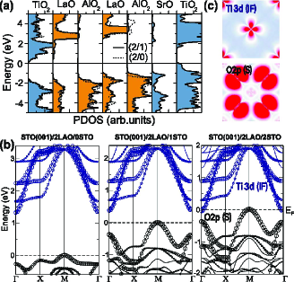
Adding a single unit-cell STO capping layer is found to have a dramatic impact on the calculated electronic structure: the band gap, being 1.2 eV for STO(001)/2LAO, is nearly closed for STO(001)/2LAO/1STO. While the ionic relaxation pattern Pentcheva and Pickett (2009) changes significantly when a capping layer is added EPA , the net contribution of the buckled TiO2 and SrO layers does not affect appreciably the total ionic dipole moment of the film (which scales with the number of LAO layers). Hence, the gap reduction has mainly an electronic origin.
The evolution of the band structure of STO(001)/2LAO/STO with increasing number of capping layers () is depicted in Fig. 1b. The valence band maximum is defined by the O -states at the M(,)-point in the surface layer, while Ti -states at at the -type interface mark the bottom of the conduction band. In the capped systems a dispersive O surface band extends 0.8 eV above the subsurface O band and effectively reduces the band gap driving the insulator-to-metal transition at an LAO thickness of only 2ML compared to 4 ML in the uncapped case. This surface state is analogous to the one on the clean STO (001) surface Kimura et al. (1995); Padilla and Vanderbilt (1998). Further STO layers (e.g. STO(001)/2LAO/2STO EPA ) increase the band overlap at the Fermi level, but have an overall weaker influence due to the lack of internal field in STO. The reduction of the band gap, and finally its closing, is thus due to three electronic effects: (i) the steady upward shift of the O states as they approach the surface Pentcheva and Pickett (2009) due to the internal polarity of LAO, (ii) the band discontinuity at the interface between LAO and the capping STO layer, and (iii) the dispersive O surface band in the capped systems that extends 0.8 eV above the subsurface O band.
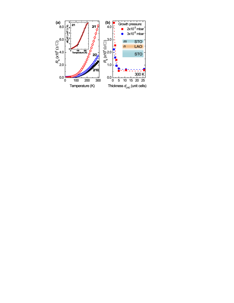
Experimentally, we confirm the crucial influence of a single monolayer of nonpolar material on the electronic interface reconstruction. STO(001)/LAO/STO samples were made by pulsed laser deposition of ML of LAO and ML of STO on TiO2-terminated STO(001) substrates (for fabrication details, see Ref. Huijben et al., 2006; Brinkman et al., 2007). While uncapped STO(001)/2LAO samples are found to be insulating (sheet resistance above 1 G), samples with an additional single ML of STO are conducting (see Fig. 2a). The conductivity is further enhanced in STO(001)/2LAO/2STO samples, but the influence of increasing the STO capping layer thickness weakens, as expected from the DFT results: the STO(001)/2LAO/10STO sample has almost the same conductivity as the STO(001)/2LAO/2STO sample. Samples with a single ML of LAO were found to be insulating except for the sample with a thick STO capping ().
It is known that the sheet resistance in STO/LAO samples depends critically on the oxygen pressure during growth Brinkman et al. (2007); Siemons et al. (2007a); Herranz et al. (2007); Kalabukhov et al. (2007); Huijben et al. (2009) and can vary over many orders of magnitude Brinkman et al. (2007). Figure 2b shows the sheet resistance for two different sets of STO/LAO/STO heterostructures with varying LAO interlayer thickness, grown at a relatively high oxygen pressure ( mbar) and at lower oxygen pressure ( mbar). For the coupled-interface samples, the influence of the oxygen pressure is now found to be much weaker. Apparently, the STO capping protects the underlying LAO surface against reconstruction via defects or adsorbates.
In order to obtain spectroscopic evidence for the electronic reconstruction, ultraviolet photoelectron spectroscopy (UPS) was performed in situ immediately after the growth of a STO(001)/2LAO/1STO sample. Figure 3a shows a gradual increase in intensity for the more surface sensitive measurements at lower detector angles. These states originate from the valence band of LAO as well as the valence band of the STO surface ML. Note, that the valence band states penetrate all the way to , unlike studies on doped STO Maus-Friedrichs et al. (2002), where only trapped states close to the conduction band are usually observed.
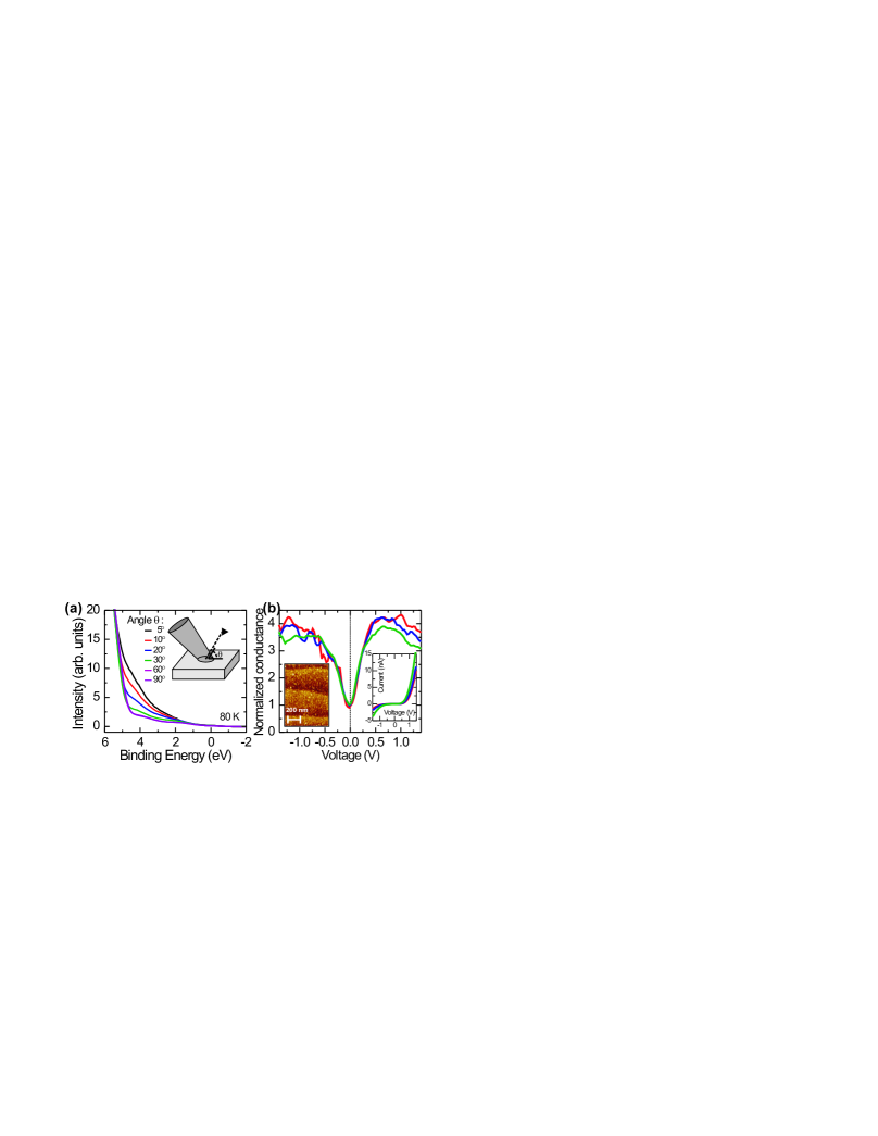
To probe states around the Fermi level, scanning tunneling spectroscopy (STS) was performed in ultra high vacuum using a variable temperature cryostat. Figure 3b shows the local density of states, , of a STO(001)/2LAO/1STO sample. At room temperature, the Fermi energy lies between the valence band of the STO surface and the conduction band of the substrate-LAO interface. The bandgap is (almost) closed, as predicted in Fig. 1 by DFT (for more spectroscopic details, see EPA ). The observed density of states just below the Fermi energy, as measured by both UPS and STS, is consistent with the electronic reconstruction scenario and suggests the presence of holes in transport.
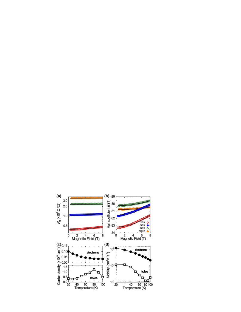
To investigate the possibility of a parallel electron-hole bilayer and the sign of the charge carriers in capped systems, magnetoresistance and Hall data were analyzed. Because the intrinsic coupling between the layers would not allow to probe the transport properties of the layers individually, unless structures are realized on a sub-micron length scale, our measurements contain information on the layers in parallel. Fig. 4 displays a positive non-quadratic magnetoresistance and a Hall resistance whose slope increases for higher fields for all conducting STO/LAO/STO samples. Quantum oscillations can still be excluded because of the low mobility. A negative magnetoresistance contribution, observed for single-interface samples deposited at high oxygen pressure Brinkman et al. (2007), only appears below 10 K. It is natural to interpret the observations in terms of multiband conductivity. Indeed, in the temperature range up to 100 K, the magnetoresistance as well as the Hall resistance can be fitted with a two band model EPA (solid lines in Fig. 4 a and b). Two carrier concentrations and two mobilities could be obtained for the STO(001)/2LAO/1STO sample from fitting as a function of temperature (Fig. 4 c and d).
The positive carrier sign of one of the bands at low temperatures indicates hole-type conductivity, while the other band is of electron-type. We note that no fit to the data could be obtained for equal signs of the two carrier densities. Neither oxygen vacancy doping, nor doping by cation substitution, have ever been shown to give rise to hole conductivity in the STO/LAO system. The calculated electron density distribution in Fig. 1c displays electrons of Ti orbital character in the interface TiO2 layer, while holes of O type are present in the surface TiO2 layer. Consequently, we attribute the hole band to the surface layer, while the electron band, with a lower carrier density but a much larger mobility, is naturally attributed to the Ti states at the interface to the substrate, consistent with the observations in Ref. Salluzzo et al. (2009).
Note, that the hole density is about an order of magnitude larger than the electron density. However, the Hall effect is dominated by the electron band because of its large mobility (103 cm2V-1s-1, similar to values obtained on single interface STO/LAO samples deposited at oxygen pressures mbar). The unequal number of electrons and holes illustrates that not all charge carriers are visible in transport measurements. While the effective electron and hole masses cannot be directly inferred from our data, the band structure calculations (neglecting strong correlation effects and defects) render 0.4 for the electrons (both in the capped and uncapped system) and a significantly higher effective mass of 1.2 for the holes. Above 100 K, neither magnetoresistance, nor a nonlinear Hall resistance were observed, because the mobilities become so low that no magnetoresistance effects are expected any longer ( in the two-band equations of EPA ). Therefore, no two-band fitting analysis can be performed in this case, and no statement can be done on the presence of electrons and holes.
In the STO(001)/2LAO/1STO sample evidence from different experimental techniques point to an electronic reconstruction mechanism. At the same time, we know that for uncapped thick LAO samples no potential build up has been observed Segal et al. (2009), suggestive of non-electronic reconstruction scenarios. In order to verify whether it is only the capping that makes a difference, the magnetotransport was studied for a large number of samples with either thicker LAO or thicker capping STO EPA . While for defect-free systems theory predicts an increase in the band overlap, and hence in the number of electrons and holes, no hole contribution was found experimentally beyond and . Apparently, during growth structural reconstruction occurs whenever the potential build up exceeds a few eV. While conductivity arises also in this case, no evidence for pure electronic reconstruction exists any longer. The STO(001)/2LAO/1STO sample might be an example of a structure where the potential build-up during the growth of just 2 ML of LAO is just not yet large enough for a reconstruction. The subsequent capping ML protects the LAO surface from structural or chemical reconstruction, provides another potential increase (either during growth or cooldown), and can accomodate mobile holes, resulting in electronic reconstruction. This conclusion provides guidelines to enhancing electronic reconstruction effects in general.
As shown in Fig. 1, the surface valence band has its maximum at the M=() zone corner, whereas the substrate-LAO interface conduction band has its minimum at the zone center. This makes the band overlap distant not only in real space (across 12 Å or more, depending on capping layer thickness) but also indirect in momentum. As a practical consequence, an electron at the surface cannot move to the substrate without some mechanism to supply the momentum transfer. The obvious mechanism is via phonons, specifically M=() phonons. These are zone boundary optical phonons, which typically lie at a few tens of meV energy. Equilibration of electrons and holes across the LAO slab will be slow at low temperature, but will occur rapidly as soon as optical phonons are excited.
In summary, the STO capping has enabled us to show that holes are present in electronically reconstructed oxide interface samples. Their mobility is low and it is expected that the holes can become localized or eliminated in uncapped STO/LAO systems more strongly (e.g. by absorbed molecules or by ionic surface reconstruction). This possibly explains the large sensitivity of uncapped samples to growth conditions and the possibility to manipulate the interface conductivity by an atomic force microscope tip Cen et al. (2008, 2009).
A further consequence of this 2D electron-hole bilayer is that it provides the conditions necessary for formation of a 2D excitonic liquid Keldysh and Kopaev (1965); des Cloizeaux (1965) comprised of interacting indirect excitons. In this oxide nanostructure the separation of the 2D electron and hole gases can be varied by the choice of polar material as well as capping material. In analogy to other oxides, such as ZnO Tsukazaki et al. (2007), it is expected that higher mobilities can be obtained by reducing the defect density. Furthermore, the carrier densities can be tuned by gating, allowing a substantial parameter range to be probed.
This work is financially supported by the Dutch Foundation for Fundamental Research on Matter (FOM), the Netherlands Organization for Scientific Research (NWO) through VIDI and VICI grants, NANONED, the Bavaria-California Technology Center (BaCaTeC), German Science Foundation (TRR80) and DOE’s Computational Materials Science Network, DOE Grant DE-FG02-04ER46111, and a grant for computational time at the supercomputer HLRBII at the Leibniz Rechenzentrum.
References
- Ohtomo and Hwang (2004) A. Ohtomo and H. Y. Hwang, Nature 427, 423 (2004).
- Ohtomo and Hwang (2006) A. Ohtomo and H. Y. Hwang, Nature 441, 120 (2006).
- Nakagawa et al. (2006) N. Nakagawa, H. Y. Hwang, and D. A. Muller, Nature Mater. 5, 204 (2006).
- Huijben et al. (2006) M. Huijben et al., Nature Mater. 5, 556 (2006).
- Thiel et al. (2006) S. Thiel, G. Hammerl, A. Schmehl, C. W. Schneider, and J. Mannhart, Science 313, 1942 (2006).
- Reyren et al. (2007) N. Reyren et al., Science 317, 1196 (2007).
- Brinkman et al. (2007) A. Brinkman et al., Nature Mater. 6, 493 (2007).
- Caviglia et al. (2008) A. D. Caviglia et al., Nature 456, 624 (2008).
- Basletić et al. (2008) M. Basletić et al., Nature Mater. 7, 621 (2008).
- Hesper et al. (2000) R. Hesper, L. H. Tjeng, A. Heeres, and G. A. Sawatzky, Phys. Rev. B 62, 16046 (2000).
- Okamoto and Millis (2004) S. Okamoto and A. J. Millis, Nature 428, 630 (2004).
- Hayward et al. (2005) S. A. Hayward et al., Phys. Rev. B 72, 054110 (2005).
- Pentcheva and Pickett (2009) R. Pentcheva and W. E. Pickett, Phys. Rev. Lett. 102, 107602 (2009).
- Ishibashi and Terakura (2008) S. Ishibashi and K. Terakura, J. Phys. Soc. Jpn. 77, 104706 (2008).
- (15) See EPAPS information.
- Kimura et al. (1995) S. Kimura, J. Yamauchi, M. Tsukada, and S. Watanabe, Phys. Rev. B 51, 11049 (1995).
- Padilla and Vanderbilt (1998) J. Padilla and D. Vanderbilt, Surf. Sci. 418, 64 (1998).
- Siemons et al. (2007a) W. Siemons et al., Phys. Rev. Lett. 98, 196802 (2007a).
- Herranz et al. (2007) G. Herranz et al., Phys. Rev. Lett. 98, 216803 (2007).
- Kalabukhov et al. (2007) A. Kalabukhov et al., Phys. Rev. B 75, 121404(R) (2007).
- Huijben et al. (2009) M. Huijben et al., Adv. Mater. 21, 1665 (2009).
- Maus-Friedrichs et al. (2002) W. Maus-Friedrichs et al., Surf. Sci. 515, 499 (2002).
- Salluzzo et al. (2009) M. Salluzzo et al., Phys. Rev. Lett. 102, 166804 (2009).
- Segal et al. (2009) Y. Segal, J. H. Ngai, J. W. Rainer, F. J. Walker, and C. H. Ahn, Phys. Rev. B 80, 241107(R) (2009).
- Cen et al. (2008) C. Cen et al., Nature Mater. 7, 298 (2008).
- Cen et al. (2009) C. Cen, S. Thiel, J. Mannhart, and J. Levy, Science 323, 1026 (2009).
- Keldysh and Kopaev (1965) L. V. Keldysh and Y. V. Kopaev, Sov. Phys. JETP 6, 2219 (1965).
- des Cloizeaux (1965) J. des Cloizeaux, J. Phys. Chem. Solids 26, 259 (1965).
- Tsukazaki et al. (2007) A. Tsukazaki et al., Science 315, 1388 (2007).