Inverse design of nanophotonic structures using complementary convex optimization
Abstract
A computationally-fast inverse design method for nanophotonic structures is presented. The method is based on two complementary convex optimization problems which modify the dielectric structure and resonant field respectively. The design of one- and two-dimensional nanophotonic resonators is demonstrated and is shown to require minimal computational resources.
1 Introduction
Numerous numerical methods have been devised to solve Maxwell’s equations in both time[1] and frequency[2, 3] domains. We refer to these schemes as direct solvers, since they compute the electric and magnetic fields based on current sources, charge distributions and surrounding dielectric and/or metallic structures. While extremely useful in simulating optical components, using direct methods to design optical components, especially in two or three dimensions, typically requires an extremely time-consuming brute force search in a large parameter space[4, 5, 6, 7, 8].
On the other hand, an inverse solver would be much more adept in such design and optimization problems[9, 10]. In this work, we define the inverse problem as that where the electromagnetic field is known, but the surrounding structure is not known. The goal in the inverse problem is, then, to find a dielectric structure that will produce that specific electromagnetic field profile.
We show that one can design nanophotonic resonators by specifying the electromagnetic field and its desirable characteristics (such as cavity quality (Q) factor and/or mode volume) and then using an inverse solver to find the corresponding dielectric structure. We show that the inverse method used is not only computationally-fast, but is also able to optimize for multiple device characteristics and produce multiple resonances, both of which are very difficult using direct methods.
2 Numerical Setup
We start from the time-harmonic eigenvalue equation
| (1) |
where , , and are the magnetic field, relative permittivity, resonance frequency and speed of light respectively. To solve the problem numerically, and are discretized in space using the standard Yee cell used in finite difference methods[1]. Also, the curl operators, since they are linear, are represented by the matrix . Eq. (1) can now be written as
| (2) |
where
In this form, given , we can solve the direct problem by computing using an eigenvalue solver[12]. However, we note that eq. (2) is also linear in , which allows us, if is held constant, to solve the inverse problem by expressing eq. (1) as
| (3) |
where
Here, is the matrix with the values of along the main diagonal and zeros elsewhere.
3 Least-Squares Method in 1D
3.1 Least-Squares
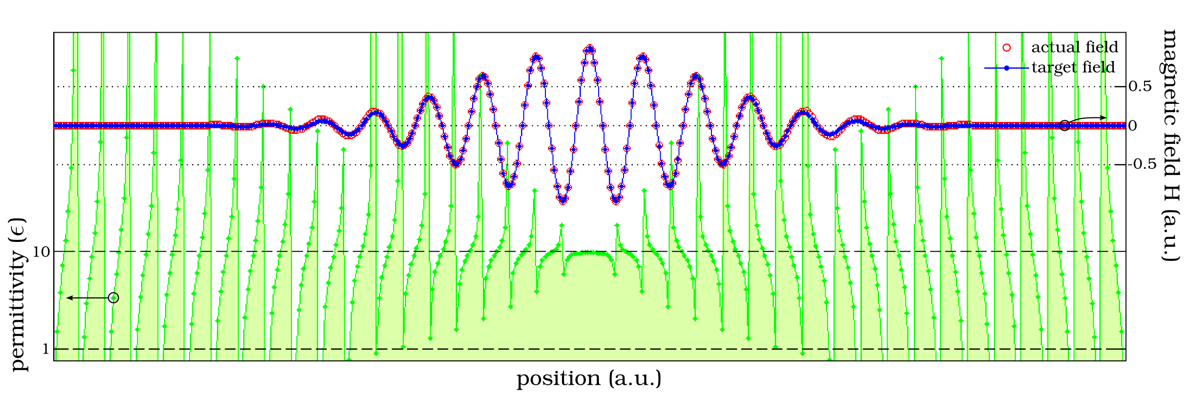
The result of applying this method to a simple one-dimensional problem is shown in Fig. 1. A generic least-squares solver [11] was used to find the dielectric structure, (green region), that exactly produces the target field, (blue line), using eq. (2). Using a generic desktop computer, the solution was obtained in less than a second. Then a finite-difference time-domain (FDTD) solver was used to obtain the actual field (red circles) produced by the structure and to verify the accuracy of .
As expected, Fig. 1 shows that the target field is reproduced exactly by the dielectric structure. However, the resulting structure is full of undesireable singularities. The rest of the section focuses on producing a well-behaved dielectric structure that still reproduces the target field accurately.
3.2 Regularized Least-Squares
The simplest way to produce a well-behaved dielectric structure is to add a regularization term to our least-squares problem,
| (4) |
which is equivalent to solving the following optimization problem
| (5) |
Here represents some initial guess for the dielectric structure, that we want the values of to stay close to.
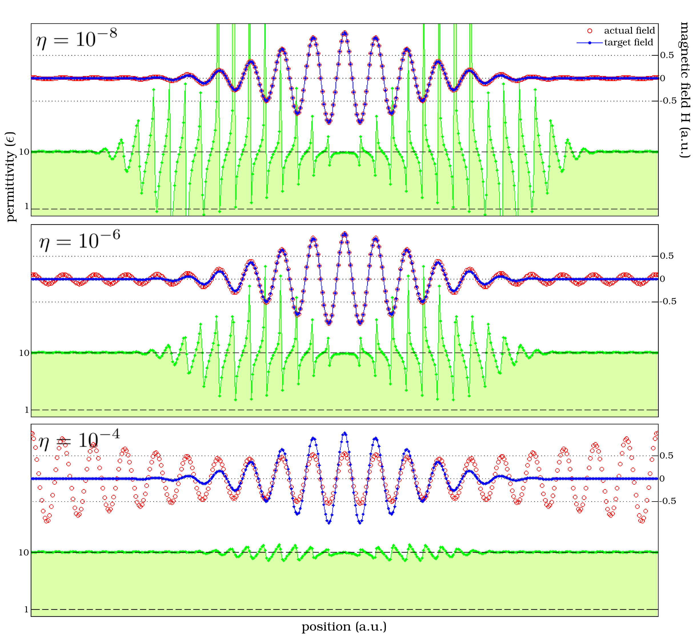
This method allows us to trade off accuracy in order to keep close to acceptable values, by increasing . We chose to constrain around a constant value of and solved the least-squares system for , , and . The results, each still obtained in under a second, are shown in Fig. 2 and illustrate the trade-off between constraining and accurately reproducing .
4 Complementary Optimization in 1D
4.1 Motivation for a Complementary Optimization Strategy
The fundamental problem in the previous examples is actually not in the methods themselves, but in the improper selection of a target field. In fact, it is very difficult to select a suitable target resonant field because not every resonant mode even has a corresponding dielectric structure that is able to reproduce it. Furthermore, it is nearly impossible to select a multi-dimensional field which corresponds to a well-behaved, isotropic and discretely-valued , as would be needed for practical structures.
For this reason, a successful method must be allowed to either modify the target field, or specify it completely, in which case the user would only determine certain characteristics (e.g. mode-volume, Q-factor) that the target field should have. The former strategy is developed in both one and two dimensions, while the latter strategy is implemented in Section 6 in order to design two-dimensional resonators with discrete values of .
4.2 Complementary Optimization
We start with the same target field as in the previous examples but we now formulate a method that allows for it to be modified during the design process. The formulation chosen is a complementary optimization routine, where we continually alternate between modifying to better fit the field, and then modifying the field to better fit . Here, we use the term “fit” to mean that either or is solved so that the residual error from eq. (1) is minimized. Additionally, both iterations are regularized in order to stably approach a solution. This algorithm can be summarized as follows,
| choose and | |||
| (6) | |||
| (7) |
where , and . is used instead of to avoid the trivial solution and does not affect the overall accuracy since changes very slowly.
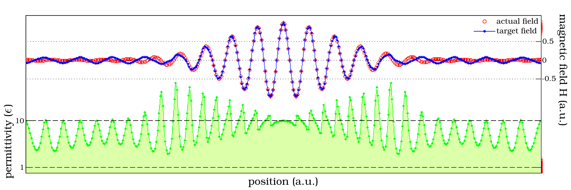
Fig. 3 shows that the complementary optimization algorithm, after iterations and with the correct choice of regularization parameters and , results in a well-behaved structure that is able to closely reproduce the modified target field. Numerically, the least-squares problem must now be solved numerous times, which increases the computational time needed to around seconds.
4.3 Complementary Optimization with Bounded
In order to achieve a more practical, discretely-valued dielectric structure, we can impose strict upper- and lower-bounds on . To this end, we modify our algorithm as such,
| choose and | |||
| (8) | |||
| (9) |
In this algorithm, eq. (8) is a convex optimization problem[13]. This allows us to impose hard constraints on , which in turn allows us to remove the regularization term present in eq. (6). The CVX package[14] is used to solve eq. (8), with each iteration of the algorithm now requiring roughly second of computation time.
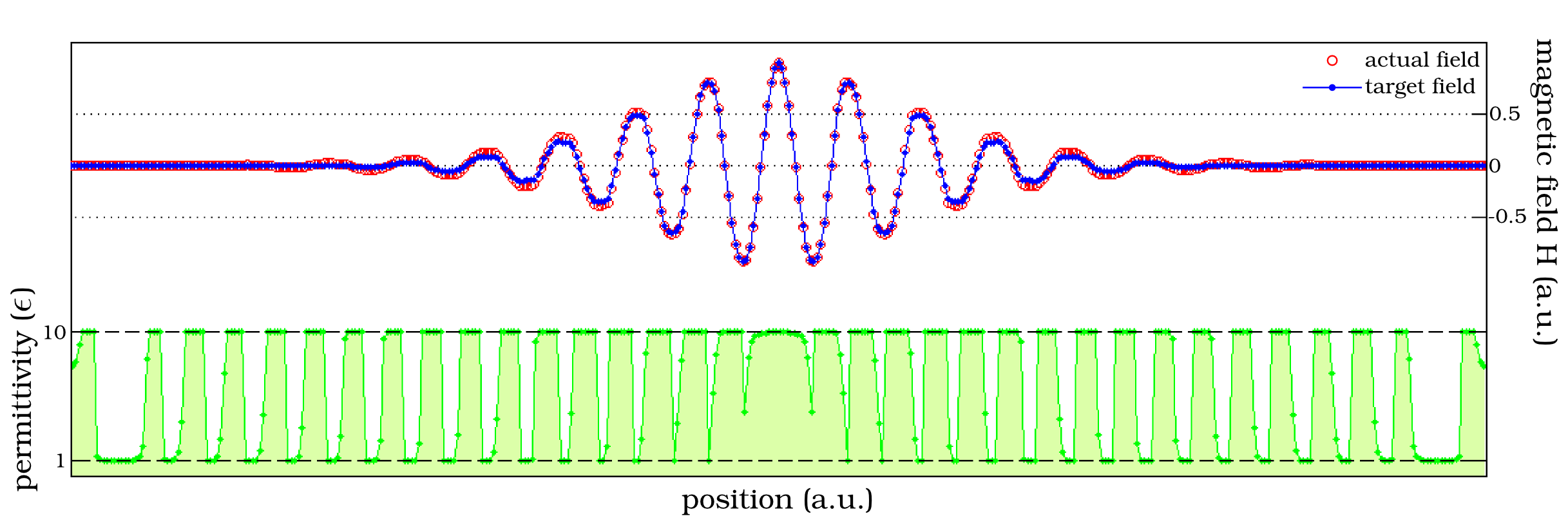
A nearly binary-valued dielectric structure is obtained in Fig. 4, which accurately produces the final target field. This is very useful for the design of practical structures, since they usually consist of two or three different materials at most. Interestingly, although the directly discreteness of was not enforced (since that would make the problem non-convex), a discrete, binary-valued structure has still arisen.
5 Complementary Optimization in 2D
5.1 “S” Resonator
We now demonstrate that the complementary optimization method is versatile and can be scaled to multiple dimensions. To ensure that is well-behaved we use a point-spread function which does not allow to change at a certain point in space without affecting the values surrounding it.
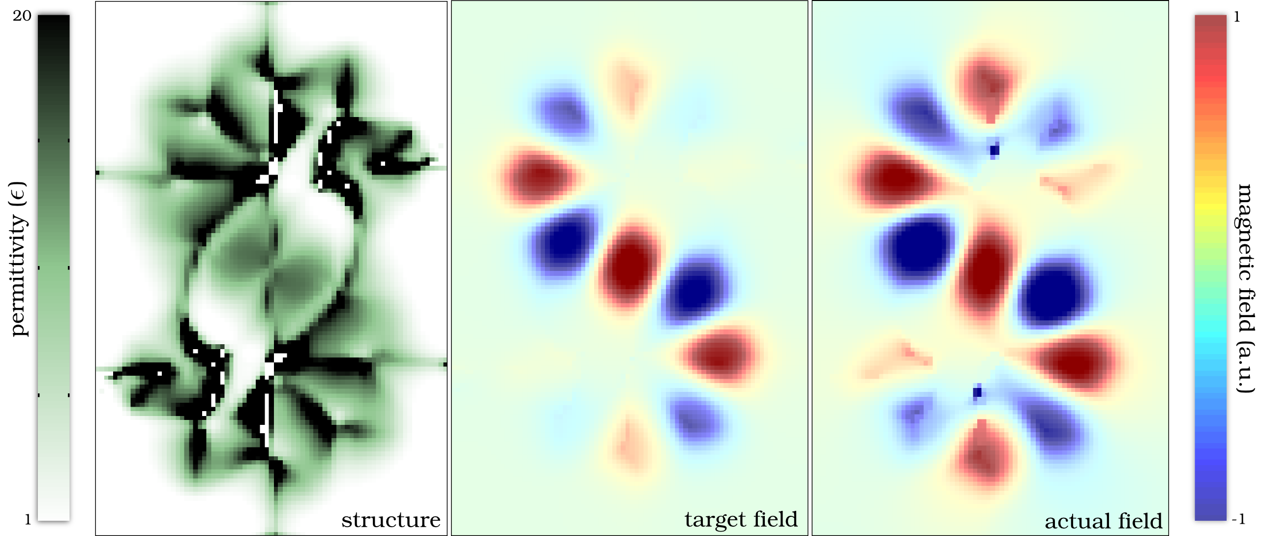
In order to show that our method can produce complex designs, we choose an S-shaped target field which is non-trivial to reproduce. The optimization results, using the complementary optimization method from Section 4.2, are shown in Fig. 5. The resulting dielectric structure is continuous, unbounded and contains some singularities (white dots), but the final target and actual fields match up well. Also, the computational cost remains quite reasonable; the iterations needed required only minutes of computation time. The resulting structure is completely unintuitive, and illustrates the kind of new capabilities offered by the inverse design strategy. Specifically, that a complex, intricate structure can be designed just by specifying the shape and frequency of a rather simple electromagnetic mode.
5.2 Multi-Mode Inverse Design
The complementary optimization method can also be extended to produce dielectric structures with multiple resonances. To do so, multiple initial target fields are specified. The dielectric structure is first modified to simultaneously fit all target fields using a multi-objective least-squares method. Then each target field is individually modified to fit the structure; and we continue alternating between optimizing and in this way. A benefit of this scheme is that only the optimization increases in size, so the design process remains computationally tractable, even for several resonant fields. This algorithm can be summarized as follows,
| choose , , , … | |||
| (10) | |||
| (11) |
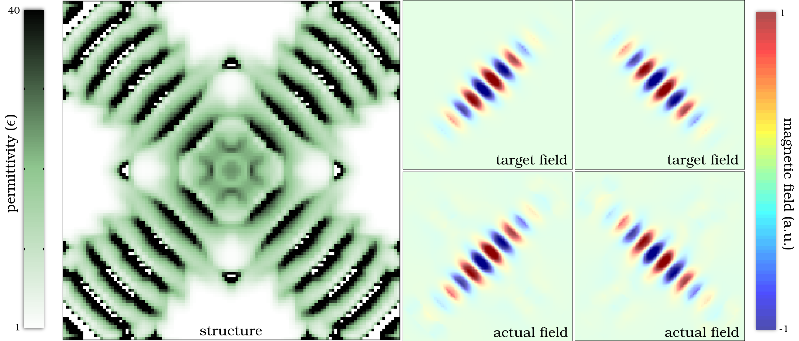
The design of an “X” resonator with two perpendicular, degenerate modes is shown in Fig. 6. The added complexity increases the total computation time to minutes for iterations of the algorithm.
5.3 Design of Waveguiding Devices
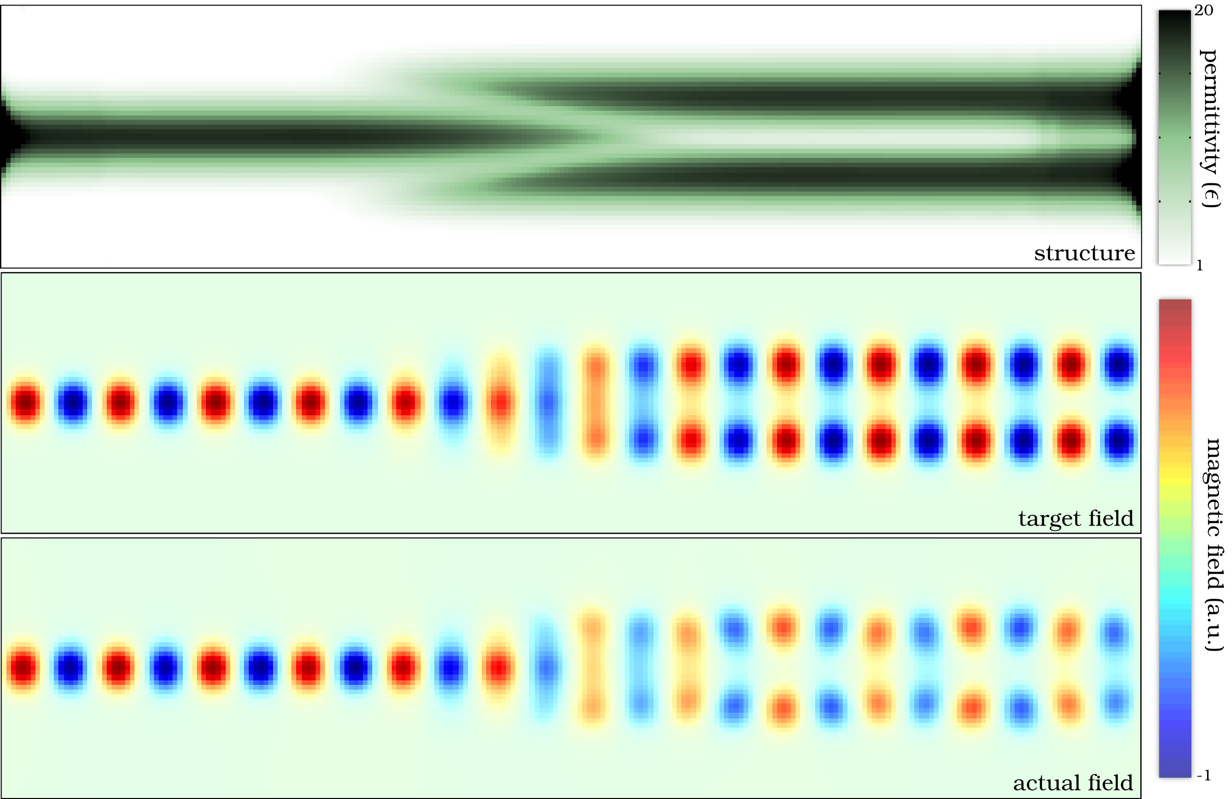
The multi-mode inverse design method can also be applied to the design of waveguiding devices such as multiplexers/demultiplexers, waveguide couplers, crossbars and dispersion-tailored waveguides. This can be accomplished by treating a waveguiding device as a doubly-degenerate resonator at its operational frequencies and then enforcing opposite symmetries (even/odd or cosine/sine) in the degenerate modes. A single-to-dual beam waveguide coupler designed based on Eq. (10) and (11) is shown in Fig. 7, and motivates how one might design other waveguiding devices such as channel-drop filters.
In addition to macroscopic waveguiding devices, one should also be able to create novel periodic waveguiding structures. For instance, by controlling the frequency of a particular waveguiding mode at each of its -vectors, one could create a waveguide with a customized dispersion characteristic, which would be useful in the design of slow-light waveguides.
6 Complementary Optimization with Bounded in 2D
6.1 Numerical Method
We now use the complementary optimization method to design resonators with discrete, binary in two dimensions. At the same time, the algorithm is modified so that we no longer specify an initial target field; instead, only an initial dielectric structure and the maximum desired mode volume (i.e. mode area in 2D) are specified. In addition, the optimization process attempts to maximize the Q-factor. Such an algorithm now consists of iteratively solving two convex optimization problem,
| choose | |||
| (12) | |||
| (13) |
In this algorithm, the field optimization, Eq. (12), differs significantly from Eq. (9). First, the eigenvalue equation term no longer utilizes . Also, a new “Fourier-minimizing” term has been added. Here, the row vectors of consist of the field Fourier components that we do not want incorporated in the final solution. The motivation for adding this term is to design high-Q resonators using planar structures, where the Q-factor is limited by out-of-plane losses, and can thus be improved by eliminating field Fourier components that are not localized by total internal reflection (components inside the light cone) [10]. Lastly, the term allows us to specify the mode area (mode volume in three dimensions), that we desire for our resonant field. This works because the two minimization objectives in Eq. (12) will generally cause the mode area to be as large as possible, which means we always end up with .
The addition of the two new terms in Eq. (12) signifies that the field iteration in our algorithm attempts to do more than to just satisfy Maxwell’s equations. Rather than only trying to fit the dielectric structure, the resonant field now also minimizes some of its Fourier components while working with a limited mode area.
In contrast with the field optimization given by Eq. (12), the structure optimization given by Eq. (13) remains identical to the equation in the one-dimensional case, Eq. (8), and contains no terms related to notions of Fourier components or mode area. In fact, the only objective in the optimization is to better fit the field generated from the field optimization. This means that in this scheme, the field iteration is leading the structure iteration. In other words, Eq. (12) “looks ahead” and gradually adapts itself to become a more desirable field, while Eq. (13) just “follows along”. For this reason, this algorithm is unique from the other complementary optimization algorithms previously presented in the article, since in those algorithms both iterations follow one another and eventually “meet in the middle”.
Finally, in this scheme, we chose to limit the degrees of freedom of both and . Some components of were fixed at non-zero values and were not allowed to be modified simply to avoid the situation. To enhance the aesthetics of the resulting dielectric structure, some components of were frozen as well, which is useful in cases where one would only like to modify the dielectric structure within a waveguide only, for example.
6.2 Circular Grating Resonator

Fig. 8 shows the design of a circular grating resonator using the method from Section 6.1. The dielectric structure emerged from a very simple choice of initial structure, namely a constant everywhere. The range of was limited to be from to , the mode area was set to and . Central components of were held constant to ensure that an electric dipole in the y-direction was produced in the center of the structure. Additionally, the components of outside a specified circle were held at a constant for the duration of the design process. The entire algorithm was run for iterations and took minutes.
After iterations, we see that a strong binary-valued structure has formed. Interestingly, the central bowtie-like structure has emerged from previous geneetic optimization methods as well[7]. Note also the extremely small amount of information needed to produce this result: only the frequency and mode area of the resonant field desired, and a trivial intial . The ability to produce a rather advanced design from such a simple problem specification highlights the potential usefulness of inverse methods in the design of novel nanophotonic devices.
6.3 Beam Resonator
The same approach was used to design a beam resonator as shown in Fig. 9. The parameters used in this design are identical to those used for the circular resonator, with the exception that the initial dielectric structure now consists of an unbroken waveguide, and the region where can be modified is now confined to the center of the waveguide.
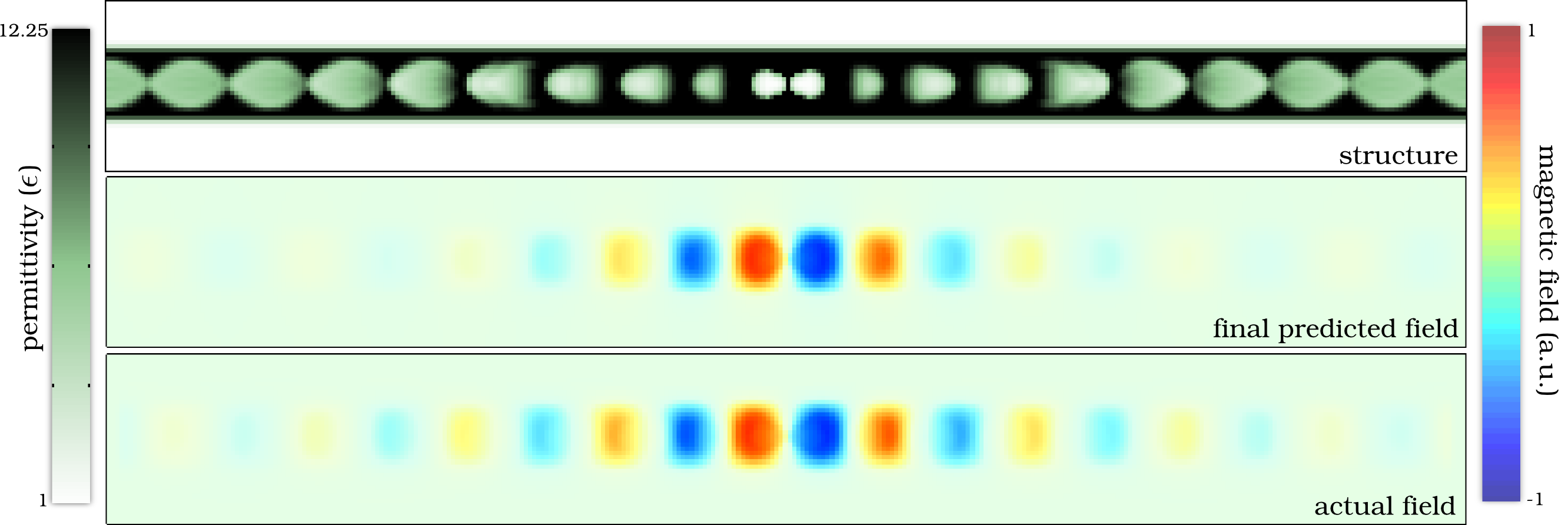
These two, simple modifications produce a vastly different result as is plainly seen from Fig. 9. Some characteristics remain, such as the two closely spaced holes in the center of the structures which focus the electromagnetic energy to a central point. Other features are unique to the beam resonator, such as a gradual outward tapering of hole diameters and size ending in a periodic “steady-state” structure, in similar fashion to Fig. 3. This tapering is a direct result of the Fourier term in Eq. (12) as it leads to a smooth field profile variation and minimization of the components in the light cone that lead to out-of-plane losses[10, 16].
7 Conclusions and Outlook
In summary, we have introduced and demonstrated a complementary optimization method for the inverse design of nanophotonic resonators as well as waveguiding structures. We have demonstrated that, in two dimensions, this method can be used to design non-trivial as well as multi-resonant structures. Furthermore, we have shown that by constraining the range of available dielectric constants, the same underlying method can produce binary-valued, discrete dielectric structures.
The methods presented here can readily be extended into three dimensions. In essence, the only hurdle is the size of the convex optimization problem for the field optimization. Since a full three-dimensional grid often consists of tens of millions of variables, solving the field optimization problem, Eq. (12), using methods such as LU factorization is no longer computationally tractable. Instead, iterative methods such as truncated Newton methods must be employed. As it turns out, such iterative methods are especially well suited to this complementary optimization scheme, since they can take advantage of the information in in order to solve very quickly. This is very applicable to our algorithm since the field changes very little from one iteration to the next.
Although solving the field optimization problem is numerically challenging in three dimensions, solving the structure optimization problem, Eq. (13), in three dimensions is much simpler. This is because only structural variations in-plane need to be accounted for planar nanophotonic devices. The number of variables in Eq. (13) for both two- and three-dimensional problems is then effectively the same, and the same numerical techniques can be employed to solve both.
A full three-dimensional inverse design method based on complementary optimization would enable the design of novel nanophotonic resonators. For instance, a resonator for efficient wavelength-conversion could be designed by creating a structure with multiple well-placed resonant frequencies [17]. Furthermore, effects such as mode overlap and the use of frequency-dependent refractive index materials could be taken into account with such a method.
Acknowledgements
This work has been supported in part by the AFOSR for Compex and Robust On-chip Nanophotonics (Dr. Gernot Pomrenke). We thank Prof. Stephen Boyd for many fruitful discussions regarding convex optimization.
References
- [1] K. Yee, “Numerical solution of initial boundary value problems involving Maxwell’s equations in isotropic media,” IEEE Trans. Antennas Propagat. 14, 302-307 (1966).
- [2] M. Albani and P. Bernardi, “A Numerical Method Based on the Discretization of Maxwell Equations in Integral Form,” IEEE Trans. on Microwave Theory 22, 446-450 (1974).
- [3] J. M. Gerardy and M. Ausloos, “Absorption spectrum of clusters of spheres from the general solution of Maxwell’s equations. The long-wavelength limit,” Phys. Rev. B 22, 4950-4959 (1979).
- [4] P. Deotare, M. McCutcheon, I. Frank, M. Khan, M. Loncar, “High quality factor photonic crystal nanobeam cavities,” Applied Physics Letters 94, 121106 (2009).
- [5] J. Vuckovic, M. Loncar, H. Mabuchi, A. Scherer, “Design of photonic crystal microcavities for cavity QED,” Physical Review E 65, 1-11 (2002).
- [6] Y. Akahane, T. Asano, B. Song, S. Noda, “Fine-tuned high-Q photonic-crystal nanocavity,” Optics Express 13, 1202-1214 (2005).
- [7] A. Gondarenko, M. Lipson, “Low modal volume dipole-like dielectric slab resonator,” Optics Express 16, 17689-17694 (2008).
- [8] A. Hakansson, J. Sanchez-Dehesa, “Inverse designed photonic crystal de-multiplex waveguide coupler,” Optics Express 13, 5440-5449 (2005).
- [9] P. Borel, A. Harpøth, L. Frandsen, M. Kristensen, P. Shi, J. Jensen, and O. Sigmund, “Topology optimization and fabrication of photonic crystal structures,” Optics Express 12, 1996-2001 (2004).
- [10] D. Englund, I. Fushman, and J. Vuckovic. “General Recipe for Designing Photonic Crystal Cavities,” Optics Express 12, 5961–5975 (2005).
- [11] CHOLMOD software package, accessed via Matlab.
- [12] S. G. Johnson, J. D. Joannopoulos, “Block-iterative frequency-domain methods for Maxwell’s equations in a planewave basis,” Optics Express 8, 967-970 (1999).
- [13] S. Boyd, L. Vandenberghe, Convex Optimization (Cambridge University Press, 2004).
- [14] M. Grant and S. Boyd, CVX: Matlab software for disciplined convex programming, http://stanford.edu/boyd/cvx, June 2009.
- [15] K. Hennessy, C. Högerle, E. Hu, A. Badolato, A. Imamoğlu, “Tuning photonic nanocavities by atomic force microscope nano-oxidation,” APL 89, 041118 (2006).
- [16] B. -S. Song, S. Noda, T. Asano, Y. Akahane, “Ultra-high-Q photonic double-heterostructure nanocavity,” Nature Materials 4, 207-210 (2005).
- [17] K. Rivoire, Z. Lin, F. Hatami, W. Ted Masselink, and J. Vuckovic, “Second harmonic generation in gallium phosphide photonic crystal nanocavities with ultralow continuous wave pump power,” Optics Express 17, 22609-22615 (2009).