4 pages, 3 figures
Spatial effects of Fano resonance in local tunneling conductivity in vicinity of impurity on semiconductor surface
Abstract
We present the results of local tunneling conductivity spatial distribution detailed theoretical investigations in vicinity of impurity atom for a wide range of applied bias voltage. We observed Fano resonance in tunneling conductivity resulting from interference between resonant tunneling channel through impurity energy level and direct tunneling channel between the tunneling contact leads. We have found that interference between tunneling channels strongly modifies form of tunneling conductivity measured by the scanning tunneling microscopy/spectroscopy (STM/STS) depending on the distance value from the impurity.
pacs:
71.55.-iI Introduction
Localized states of individual impurity atoms play the key role in tunneling processes in small size junctions and often determine the behavior of tunneling characteristics in STM/STS contacts. Investigation of tunneling through impurity atom energy level reveal interesting phenomena such as resonant tunneling, interference between resonant and direct tunneling channels, Kondo effects in quantum dots strongly coupled with the leads of tunneling contact Konig and Fano-type line shapes in the situation of multichannel transport Fano ; Gores . Influence of different impurities on the tunneling conductivity was widely studied experimentally and theoretically. Most of the experiments were carried out with the help of scanning tunneling microscopy/spectroscopy technique Dombrowski ; Boon ; Maslova ; Panov , but experimental measurements provides no information weather electron transport occurs coherently or incoherently. Answer to this question can be found from the comparison between experimental and theoretical results. Theoretical investigations of single impurities influence on tunneling conductivity mostly deals with Green’s functions formalism Hofstetter ; Konig .
Usually theoretical calculations of interference effects between resonant and direct tunneling channels correspond to the case when metallic STM tip is positioned above the impurity atom Hofstetter ; Konig . However experimentally tunneling conductivity can be measured far away from the impurity Madhavan and just this case is quite of great interest because it gives an opportunity to initialize impurities types. So in our work we present formula, which describe spatial distribution of local tunneling conductivity in vicinity of impurity in the case of interference between resonant and direct tunneling channels. We found that taking into account real part of impurity Green’s function leads to drastical changing of the tunneling conductivity form depending on the values of tunneling rates and distance.
II The suggested model and main results
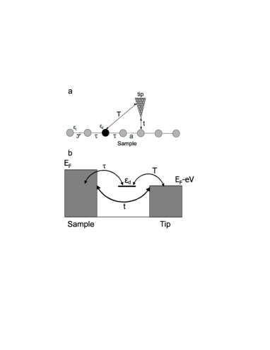
We shall analyze tunneling between semiconductor surface ( atomic chain) and metallic STM tip (Fig. 1a). atomic chain is formed by the similar atoms with energy levels and similar tunneling transfer amplitudes between the atoms along the atomic chain. Distance between the atoms in the atomic chain is equal to . Atomic chain includes impurity with energy , tunneling transfer amplitude from impurity atom to the nearest atoms of the atomic chain is . Tunneling conductivity is measured by the STM tip. Direct tunneling between the surface continuous spectrum states and tip states is described by the transfer amplitude . Tunneling from the impurity energy level to the tip is described by tunneling transfer amplitude . The model of tunneling contact formed by semiconductor and metallic tip is depicted in Fig. 1b.

The model system can be described by the Hamiltonian: :
| (1) | |||||
Indices and label the states in the left (semiconductor) and right (tip) lead, respectively. The index indicates that impurity electron operator is involved. is a typical Hamiltonian for atomic chain with hoppings without any impurities. describes resonant tunneling transitions from the impurity state to the semiconductor and metallic tip and direct transitions between the tunneling contact leads. corresponds to the electrons in the localized state formed by the impurity atom in the atomic chain, describes conduction electrons in the metallic tip.
We shall use diagram technique in our investigation of tunneling conductivity spatial distribution Keldysh . Using Keldysh functions the tunneling current from the right lead can be determined as (we set charge ):
| (2) |
where is tunneling ”response function”.
The first (second) part of the Eq. 2 describes electron transfer from the right lead to the impurity (to the left lead) or vice versa. Our aim is to re-write Keldysh functions and in the terms of retarded and advanced Green’s functions. We can do it with the help of Dyson-like equations
| (3) |
for the function and equations
| (4) |
for the function .
To evaluate the dependence of local tunneling conductivity on the distance from the impurity one have to write instead of tunneling transfer amplitude the expression which takes into account spatial distribution of tunneling conductivity (x-distance from the impurity along the atomic chain). Substituting the correspondent expressions for the Keldysh functions, received from equations 3, 4 to the tunneling current equation 2, performing summation over and and taking imaginary part we get the expression for the local tunneling conductivity:
| (5) | |||||
where impurity retarded Green’s function is defined by the expression:
| (6) |
Relaxation rates , are determined by electron tunneling transitions from localized states to the leads and continuum states and relaxation rate corresponds to direct tunneling transitions between and continuum states ; ; .
is unperturbed density of states in semiconductor. Expression for can be found from the dispersion law of the atomic chain which has the form
| (7) |

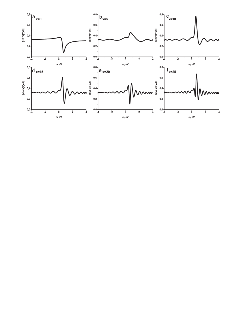
Figures 2 and 3 show tunneling conductance as a function of applied bias voltage for different values of distance from the impurity and different values of tunneling transfer amplitudes. Figure 2 corresponds to the case when value of direct tunneling channel transfer amplitude exceeds values of resonant tunneling channel transfer amplitudes through the impurity energy level and . In this case tunneling conductivity calculated above the impurity (Fig. 2a) has Fano line shape due to interference between resonant and nonresonant tunneling channels. Tunneling conductivity shows a dip when applied bias voltage is equal to the impurity energy level position . The degree of asymmetry of the resonant line shape depend on the relative strengths of transmission through the two channels. When the distance value is not equal to zero a series of dips in the local tunneling conductivity exist. Amount of dips increases with the increasing of distance value. When applied bias voltage is equal to the impurity energy level position (resonance) not only a dip (Fig. 2a,e) but also a peak (Fig. 2b,f) can exist in the tunneling conductivity measured aside from the impurity. At the fixed parameters of the atomic chain such as tunneling transfer amplitudes existance of a dip or a peak in tunneling conductivity in the resonance is determined by the value of the distance. At the special values of distance it can be neither resonance dip nor resonance peak (Fig. 2d). Replacement of the dip by the peak in tunneling conductivity when applied bias voltage is equal to the impurity energy level position is the result of interference between the direct and resonant tunneling channels (between real and imaginary parts of impurity Green’s functions).

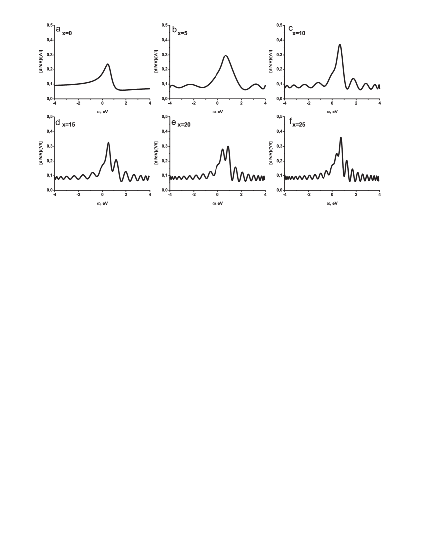
Figure 3 shows tunneling conductance as a function of applied bias voltage in the case when values of resonant tunneling channel transfer amplitudes through the impurity energy level and exceed transfer amplitude of direct tunneling channel . In this case formation of a asymmetric peak in tunneling conductivity calculated above the impurity (Fig. 3a) in the resonance when applied bias voltage is equal to the impurity energy level position can be seen in the tunneling conductivity. With increasing of distance value resonant peak still exists but it’s shape changes due to the effects caused by the interference between tunneling channels (Fig. 3b,c). Simultaneously formation of non-resonance dips in local tunneling conductivity is found with the increasing of distance.
Further increasing of distance value leads to formation of the resonance dip when applied bias voltage is equal to the impurity energy level position (Fig. 3d-f). From the other hand dip’s formation can be interpreted as resonance peak splitting. Dip’s amplitude depends on the distance value and it decreases with the distance increasing at the fixed values of tunneling rates in the system. More over with increasing of the distance interference between the direct and resonant tunneling channels influence the amplitudes of the peaks formed by resonant peak splitting. Amplitude of the peak which corresponds to the lower value of applied bias voltage decreases with increasing of the distance value from the impurity. Amplitude of the peak which corresponds to the higher value of applied bias voltage increases with increasing of the distance value from the impurity Fig. 3d-f).
III Conclusion
In this work we have studied the influence of interplay between the resonant tunneling channel through the impurity energy level and direct tunneling channel between the leads of tunneling contact on local tunneling conductivity. It was found that depending on the value of the distance from the impurity special features can be seen in tunneling conductivity, such as dip or peak when applied bias voltage is equal to the impurity energy level position. When value of direct tunneling channel transfer amplitude exceeds values of resonant tunneling channel transfer amplitudes through the impurity energy level tunneling conductivity calculated above the impurity has Fano line shape due to interference between resonant and nonresonant tunneling channels. With increasing of the distance from the impurity a series of dips are formed in local tunneling conductivity in spite of a dip or a peak exists in the resonance. We derived replacement of the dip by the peak as a result of interference between the direct and resonant tunneling channels.
Replacement of the peak by the dip and vice versa can be observed experimentally with the help of STM/STS technique as impurity atom switching on and off in local tunneling conductivity.
This work was supported by RFBR grants and by the National Grants for technical regulation and metrology.
References
- (1) J. Konig, H. Schoeller, G. Shone, Phys. Rev. Lett., 76, 1715, (1996)
- (2) U. Fano, Phys. Rev., 1244, 1866, (1961)
- (3) J. Gores, D. Goldhaber-Gordon, S. Heemeyer et al., Phys. Rev. B, 62, 2188, (2000)
- (4) R. Dombrowski, C. Wittneven, M. Morgenstern et al., Appl. Phys. A, 66, S203-S206, (1998)
- (5) J. Inglesfield, M. Boon, S. Crampin, Condens. Matter, 12, L489-L496, (2000)
- (6) N.S. Maslova, V.I. Panov, V.V. Rakov et al., Appl. Phys., A66, 171, (1998)
- (7) N.S. Maslova, V.I. Panov, S.V. Savinov et al., Phys. Rev. , B60, 2619, (1999)
- (8) W. Hofstetter, J. Konig, H. Schoeller, Phys. Rev. Letters, 87, 156803, (2001)
- (9) J. Konig, Y. Gefen, Phys. Rev. Letters, 86, 3855, (2001)
- (10) V. Madhavan, W. Chen, T. Jamneala et al., Science, 280, 567, (1998)
- (11) L.V. Keldysh, Sov. Phys JETP, 20, 1018, (1964)