Electron tunnel rates in a donor-silicon single electron transistor hybrid
Abstract
We investigate a hybrid structure consisting of implanted 31P atoms close to a gate-induced silicon single electron transistor (SiSET). In this configuration, the SiSET is extremely sensitive to the charge state of the nearby centers, turning from the off state to the conducting state when the charge configuration is changed. We present a method to measure fast electron tunnel rates between donors and the SiSET island, using a pulsed voltage scheme and low-bandwidth current detection. The experimental findings are quantitatively discussed using a rate equation model, enabling the extraction of the capture and emission rates.
pacs:
73.20.Hb, 73.21.La, 73.23.HkThe readout of a single spin is one of the key elements in spin-based quantum information processing schemes Kane (1998); Cerletti et al. (2005). One may distinguish between single-shot readout, where the projective measurement of a single spin is performed in real time, and “spectroscopic” readout, where the expectation value of the spin state is deduced from a time-averaged quantity (e.g. electrical current, fluorescence emission, …). Single-shot readout has been demonstrated in GaAs/AlGaAs quantum dots Elzerman et al. (2004); Barthel et al. (2009), while spectroscopic readout has been obtained in a variety of systems, from quantum dots Hanson et al. (2007); Berezovsky et al. (2006); Shaji et al. (2008); Liu et al. (2005); Xiao et al. (2004) to NV centers in diamond Jelezko et al. (2004) and dopant atoms in silicon Sellier et al. (2006). Carbon and silicon are particularly attractive platforms for solid-state spin-based quantum processors, because they can be isotopically purified to minimize decoherence induced by nuclear spins. However, single-shot readout in these systems has not yet been demonstrated. Recently, an architecture for single-shot readout of a donor spin in silicon was proposed Morello et al. (2009), consisting of a single implanted P donor Jamieson et al. (2005) in close proximity to an induced silicon single-electron transistor (SiSET) Angus et al. (2007). The approach employs a readout principle similar to the one successfully demonstrated in GaAs/AlGaAs single quantum dots Elzerman et al. (2004), where the spin state of the electron is deduced from the time-resolved observation of spin-dependent tunneling between the dot and a charge reservoir. However, in the donor-based proposal Morello et al. (2009), the bulk charge reservoir is replaced by the island of a SiSET. This configuration is predicted to yield very large charge transfer signals, thereby allowing high-fidelity single-shot spin readout. The timescale of the projective spin measurement is set by the electron tunneling time between donor and SiSET, which must be controlled and understood before attempting spin readout.
In this Letter we demonstrate and investigate the tunneling of electrons in a hybrid device, consisting of approx. 31P donors, implanted next to an induced SiSET. We show that the current through the SiSET, , can be switched from zero to the maximum value by transferring an electron from a charge center to the SET island. By applying voltage pulses to a gate near the donors while monitoring , we study the probability for an electron to tunnel between the center and the SiSET. The resulting change in can be understood by considering the donor-SET hybrid system as analogous to a double quantum dot in the parallel configuration Hofmann et al. (1995). We find that the amplitudes in a pattern of Coulomb peaks depend on the pulse duration and duty cycle, relative to the emission and capture rates for tunneling from or onto the donor. Employing a rate equation model, we are able to extract the electron tunneling rate for a specific charge center. We observe fast tunneling rates of 3000 s-1 for the tunnel event to load the center and 1000 s-1 for the reverse process, despite the detection bandwidth for the SET (DC) readout being limited to 200 Hz.
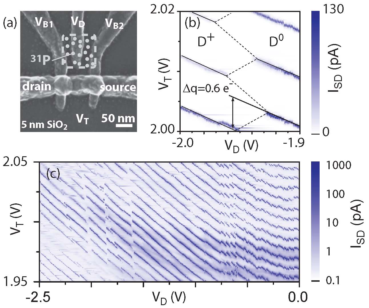
Figure 1 (a) shows the device fabricated on a high purity intrinsic silicon wafer ( kcm), with the implantation sites (grey dots) located next to an induced SiSET Angus et al. (2007, 2008). In the active device region a high-quality, 5 nm thick silicon oxide is grown by dry thermal oxidation, yielding a very low density of interface traps /eV/cm2 near the conduction band edge Johnson et al. (2009). Underneath this oxide ohmic contacts are provided ([P]5 cm-3). In a first electron beam lithography (EBL) step, with subsequent development and evaporation, Ti(15 nm)/Pt(65 nm) alignment markers are formed for a high precision ( nm) realignment of subsequent layers. A aperture is opened in the PMMA resist, acting as mask for the 31P donors, which are implanted with an acceleration voltage of 14 keV and at a fluence of cm-2, resulting in a total of 31P donors in this region. After a rapid thermal anneal (1000 ∘C, 5 s) to repair the implantation damage, the Al donor control gate as well as the Al barrier gates of the SiSET are patterned. The surface of these gates is oxidized by an O2 plasma ash for 4 min at 180∘C, resulting in a nm thick AlxOy insulating layer Lim et al. (2009). An Al top-gate, overlaying the barriers and the source-drain regions, is formed in the last EBL step. This process results in a hybrid quantum system with a few 31P donors in close vicinity to a SiSET. The sample is operated in a dilution refrigerator at an electron temperature mK. The source, drain, as well as the SiSET control gates are connected to the room temperature electronics via Cu powder filters with a cut off frequency GHz. The donor control gate is connected via a high-bandwidth line to apply high frequency pulses ( kHz, limited by resistive voltage dividers at room temperature). Its voltage is the sum of a constant component plus a rectangular wave for pulsed voltage spectroscopy. The SiSET DC source-drain current is measured using a current amplifier with 200 Hz bandwidth and a gain of 1010V/A.
The capacitively- and tunnel-coupled donor and the SiSET island effectively form a double quantum dot in parallel configuration Hofmann et al. (1995). Both series and parallel configurations result in a hexagonal stability diagram, but in the series configuration, transport only occurs at the triple pointsvan der Wiel et al. (2003). In contrast, in the parallel configuration the transport channel is open for any gate voltages for which the electrochemical potential of the SiSET, , resides in the source-drain bias window. As a result, transport occurs along some of the lines that connect the triple points, which we call transport-lines in the following. Fig. 1 (b) shows these transport-lines in the vicinity of a charge transition, measured with a source-drain bias 50 V. The relevant gate space is defined by the top-gate () of the SiSET and the donor control gate (). When the energy level of the donor is raised with respect to , at the charge transition point it becomes favorable to remove an electron. This change in the charge configuration (here labeled as transition) acts back on and results in a shift of the Coulomb peak lines. The magnitude of the shift in , relative to the Coulomb peak spacing, is quantified by the charge transfer signal . Since is much larger than the width of the Coulomb peaks, is switched from zero to its maximum value by changing the occupancy of the charge center. The data in Fig. 1 (b) demonstrate the ability to resolve with essentially 100% contrast the charge state of the donor, a critical prerequisite for the spin readout method proposed in Ref. Morello et al., 2009.
As shown in Fig 1 (c), the measurement of as a function of and yields a set of Coulomb peaks appearing as tilted lines (due to the cross-capacitance between control gate and SET island) that break at the charge transition points. For - V the slope of the transport-lines decreases, indicating charge accumulation under the donor control gate. In this regime we find several small charge transitions with , which we interpret as the ionization of shallow charge centers to the Si/SiO2 interface. At more negative voltages, the pattern clears up, showing well-isolated charge transfers with 0.2 0.6 in agreement with the predicted values for electrons tunneling into the SET island from donors nm away Morello et al. (2009), and similar to the values observed in Sun and Kane (2009) for a charge center near Al- and Si-SETs. This part of the stability diagram is stable and reproducible upon thermal cycling to room temperature.
We stress that the parallel geometrical configuration of our hybrid device impedes direct spectroscopy of the charge center coupled to the SiSET. It is therefore impossible to distinguish a donor from e.g. an interface trap on the basis of its energy levels structure Lansbergen et al. (2008). The number of charge transitions observed for -0.6 V is compatible with the number of donors expected to be found within 30 to 50 nm from the SET island, given the P implant fluence. Furthermore, we note that the charge transitions in this regime typically group in pairs, agreeing in and slope in the - gate space, again compatible with the observations of P donors with two charge transition levels expected Sellier et al. (2006); Ramdas and Rodriguez (1981). However, the unambiguous identification of the charge center remains a quest for spin readout in combination with magnetic resonance techniques Morello et al. (2009). In this letter, the main focus is on the study of tunnel rates between a SiSET and a charge center, whose precise nature does not affect the results.
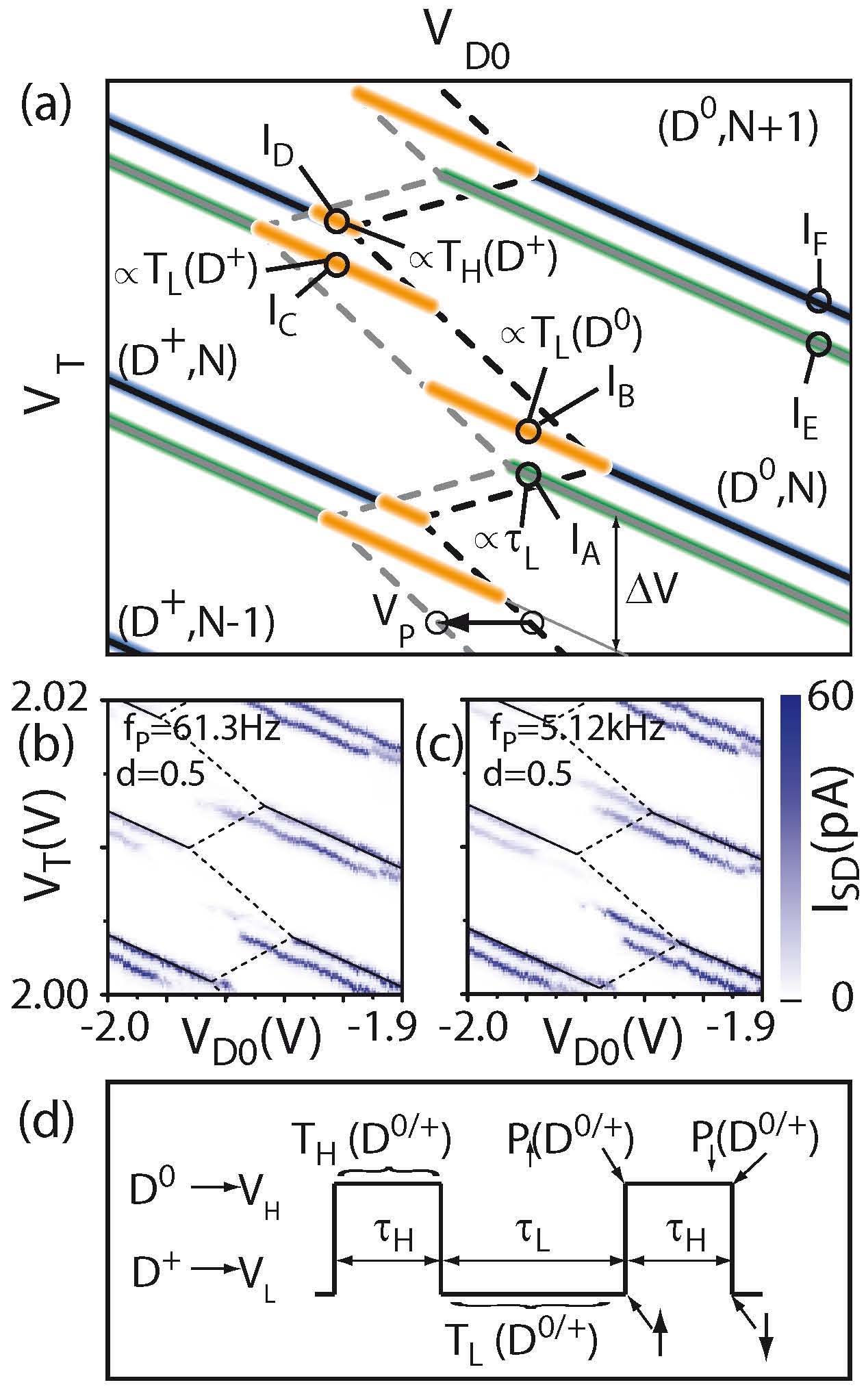
We measure the tunnel rates by superimposing on the DC voltage of the donor control gate () a rectangular wave with frequency , duty cycle , and amplitude (cf. Fig. 2 (d)). If is slow compared to the (de)charging rate of the center, we record two stability diagrams (blue and green in Fig. 2 (a)), offset by on the horizontal axis when plotted vs. the DC gate voltages and . These arise because any point on the diagram probes the average for the combination of the gate voltages and . Conversely, if is faster than the electron tunnel rate to/from the charge center, we find at gate configurations where transport would be otherwise suppressed, which we call non-equilibrium transport-lines in the following (cf. orange lines in Fig. 2), in addition to the pure shifting of the pattern along the -axis. These lines arise because the charge center retains its configuration for the time-span determined by the tunneling time, even while its chemical potential crosses the charge transition point. To be specific, at (cf. Fig. 2 (a)) no current is expected for the configuration, the equilibrium state at . When the additional voltage pulse is in the high state, the chemical potential is pushed over the charge transition point, into the region where is the equilibrium configuration. If an electron is captured (and is occupied) during this time, immediately after is brought back to zero we will find the state at a gate configuration where a transport-line is present. Thus, when , until the electron tunnels out again. Observing a DC current in the orange shaded area around indicates that the system is able to maintain a non-equilibrium state for a time comparable to the pulse duration, i.e. the tunnel rate is comparable to the pulsing frequency . Similar arguments hold for and , whereas the bias line around is not altered, because the voltage pulse does not cause a charge transition of the center. Note that this symmetry break stems from the asymmetric pulsing between 0 V and . The low-frequency limit is shown in Fig. 2 (b), where Hz, and only a horizontally-shifted duplicate of the Coulomb peaks pattern is observed. In contrast, the data in Fig. 2 (c) illustrate the high-frequency limit kHz, where we find at the location of non-equilibrium transport lines.
Quantitatively, the DC value of at the non-equilibrium current peaks can be understood within a rate equation model. When we pulse the chemical potential of the charge center over the charge transition level, the current state D+/0 will either persist, because the stable state is reached, or change to the opposite state with the corresponding capture () or emission () rate. The probability to find at the point in Fig. 2 (d) the state occupied is , because during the system tends towards . Additionally, , because is increased during . The same arguments hold for the inverse direction yielding and . To determine the four separate time durations, corresponding to occupation of either or , for both values or , which we label ) we express the probabilities as a function of and . We integrate these probabilities, including the time evolution of the occupation of the charge state over the pulse length , to obtain the average time, finding during . The result is the four times of interest: , , , and , where .
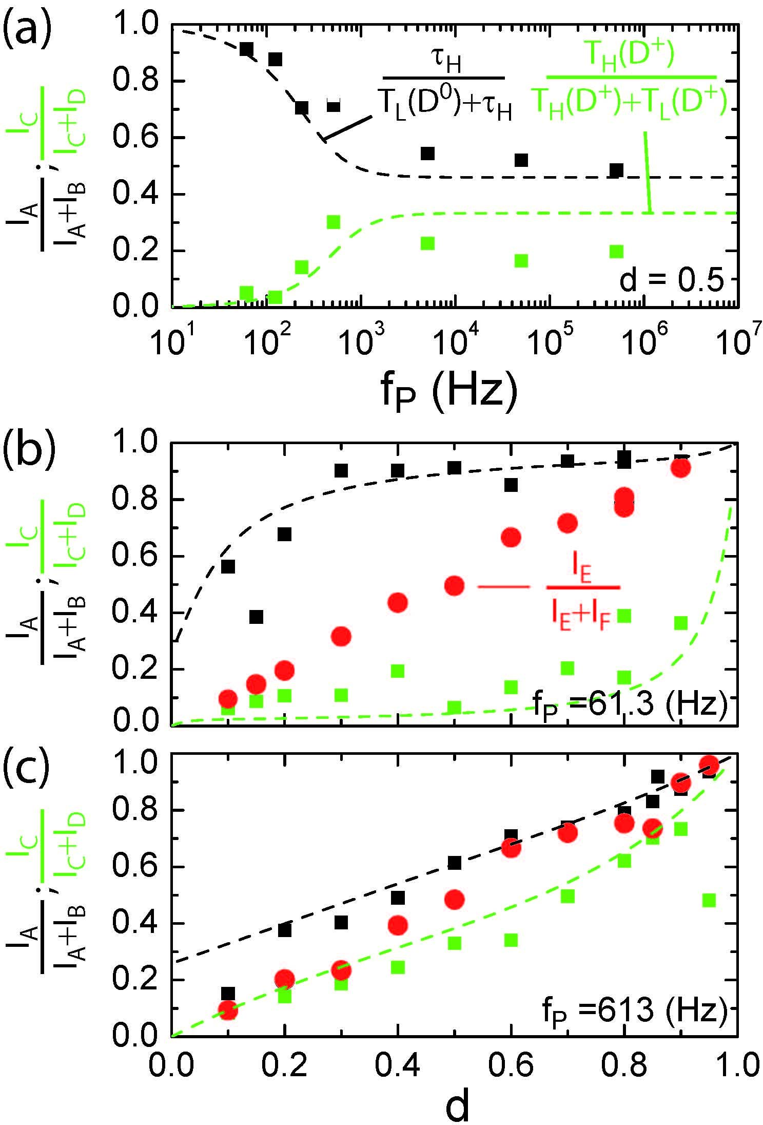
The times obtained in this manner are proportional to . Since every transport-line has an individual current amplitude, we analyze the peak ratios and which are equal to the ratios and , respectively. Although pulsing is performed parallel to the control gate axis, it is possible to compare current amplitudes from a cut along the top-gate axis, because the current amplitude does not vary significantly along specific transport-lines. Figure 3 (a) displays the peak ratios for a duty cycle of as function of . The ratios (black squares) and (green squares) are obtained from data like Fig. 2 (b) or (c) and both show a quantitative agreement with the model using s-1 and s-1 over the entire frequency range . Fig. 3 (b) compares the model with the experimental data for a fixed Hz as a function of the duty cycle . Again, the data is described well by the model using the same capture and emission rates. At and , the peak ratios are more difficult to determine due to the low for one of the contributions, explaining the deviations from the model. For comparison, the duty cycle (red circles in Fig. 3 (b),(c)) is recovered from the spectra independently by analyzing the ratio , showing good agreement with the duty cycle applied. Fig. 3 (c) shows the same plot as Fig. 3 (b) for a higher Hz, again in good agreement with the model.
An estimate of the distance between the charge center and the SET island can be obtained from the capacitive modeling of the charge transfer signal , as shown in Ref. Morello et al., 2009. For the specific geometry of the device measured here, we find that corresponds to a distance nm. We use ISE-TCAD to calculate the profile of the conduction band between donor and SET when the state is aligned with , and from this, the area of the tunnel barrier. A WKB calculation of the tunnel rate yields s-1, in reasonable agreement with experimental findings.
In summary, we demonstrated and analyzed the tunneling of electrons in a hybrid device consisting of 31P donors implanted next to a gate-induced SiSET. We showed that the changes in the surrounding charge configuration can be sensitively detected by the SET, and the mutual coupling fulfills the requirements necessary for spin readout as proposed in Ref. Morello et al. (2009). We further demonstrated a technique to determine the tunnel rate of the center investigated, and this technique is applicable even when this tunnel rate exceeds the bandwidth of the detection SET. We also provide a quantitative tunnel rate model that agrees with the experimental findings. This experimental and theoretical toolbox paves the way to the use of spin-dependent electron tunneling as a readout method for single spins in silicon.
The authors thank D. Barber, N. Court, E. Gauja, R. P. Starrett, and K. Y. Tan for technical support at UNSW, and Alberto Cimmino for technical support at the Univ. of Melbourne. This work is supported by the Australian Research Council, the Australian Government, and by the U.S. National Security Agency (NSA) and U.S. Army Research Office (ARO) under Contract No. W911NF-08-1-0527. Work at Wisconsin was supported by ARO and LPS under Contract No. W911NF-08-1-0482.
References
- Kane (1998) B. E. Kane, Nature 393, 133 (1998).
- Cerletti et al. (2005) V. Cerletti et al., Nanotechnology 16, R27 (2005).
- Elzerman et al. (2004) J. M. Elzerman et al., Nature 430, 431 (2004).
- Barthel et al. (2009) C. Barthel et al., Phys. Rev. Lett. 103, 160503 (2009).
- Hanson et al. (2007) R. Hanson et al., Rev. Mod. Phys. 79, 1217 (2007).
- Berezovsky et al. (2006) J. Berezovsky et al., Science 314, 1916 (2006).
- Shaji et al. (2008) N. Shaji et al., Nature Physics 4, 540 (2008).
- Liu et al. (2005) H. W. Liu et al., Phys. Rev. B 72, 161305(R) (2005).
- Xiao et al. (2004) M. Xiao et al., Nature 430, 435 (2004).
- Jelezko et al. (2004) F. Jelezko et al., Phys. Rev. Lett. 92, 076401 (2004).
- Sellier et al. (2006) H. Sellier et al., Phys. Rev. Lett. 97, 206805 (2006).
- Morello et al. (2009) A. Morello et al., Phys. Rev. B 80, 081307(R) (2009).
- Jamieson et al. (2005) D. N. Jamieson et al., Appl. Phys. Lett. 86, 202101 (2005).
- Angus et al. (2007) S. J. Angus et al., Nano Lett. 7, 2051 (2007).
- Hofmann et al. (1995) F. Hofmann et al., Phys. Rev. B 51, 13872 (1995).
- Angus et al. (2008) S. J. Angus et al., Appl. Phys. Lett. 92, 112103 (2008).
- Johnson et al. (2009) B. C. Johnson et al., Thin Solid Films, doi:10.1016/j.tsf.2009.09.152 (2009).
- Lim et al. (2009) W. H. Lim et al., Appl. Phys. Lett. 94, 173502 (2009).
- van der Wiel et al. (2003) W. G. van der Wiel et al., Rev. Mod. Phys. 75, 1 (2003).
- Sun and Kane (2009) L. Sun and B. E. Kane, Phys. Rev. B 80, 153310 (2009).
- Lansbergen et al. (2008) G. P. Lansbergen et al., Nature Physics 4, 656 (2008).
- Ramdas and Rodriguez (1981) A. K. Ramdas and S. Rodriguez, Reports on Progress in Physics 44, 1297 (1981).