Quantum Transport in an Array of Mesoscopic
Rings: Effect of Interface Geometry
Paramita Dutta†, Santanu
K. Maiti†,‡,111Corresponding Author: Santanu K.
Maiti
Electronic mail: santanu.maiti@saha.ac.in
and S. N. Karmakar†
†Theoretical Condensed Matter Physics Division,
Saha Institute of Nuclear Physics,
1/AF, Bidhannagar, Kolkata-700 064, India
‡Department of Physics, Narasinha Dutt College,
129 Belilious Road, Howrah-711 101, India
Abstract
Electron transport properties are investigated in an array of mesoscopic rings, where each ring is threaded by a magnetic flux . The array is attached to two semi-infinite one-dimensional metallic electrodes, namely, source and drain, where the rings are considered either in series or in parallel configuration. A simple tight-binding model is used to describe the system and all the calculations are done based on the Green’s function formalism. Here, we present conductance-energy and current-voltage characteristics in terms of ring-to-electrode coupling strength, ring-electrode interface geometry and magnetic flux. Most interestingly it is observed that, typical current amplitude in an array of mesoscopic rings in the series configuration is much larger compared to that in parallel configuration of those rings. This feature is completely different from the classical analogy which may provide an important signature in designing nano-scale electronic devices.
PACS No.: 73.63.-b; 73.63.Rt
Keywords: A. Mesoscopic rings; A. AB flux; D. Conductance; D. - characteristic.
1 Introduction
Study of quantum transport in low-dimensional systems has begun to flourish during the past few decades. All the basic features of electron transport in such systems solely depend on the concept of quantum interference effect, and it is generally preserved throughout the sample only for much smaller sizes, while the effect disappears for larger systems [1, 2]. A normal metal mesoscopic ring is a very nice example where the electronic motion is confined and the transport becomes predominantly coherent [3, 4, 5]. Several exotic phenomena are observed in such a ring system [6, 7, 8], especially in presence of magnetic flux, due to the effect of quantum interferences. In a very recent paper, Peeters et al. [9] have revealed this fact by doing a nice work on an array of mesoscopic rings. At thermodynamic equilibrium, electrons in a mesoscopic ring, threaded by magnetic flux , can support non-decaying current even at non-zero temperature. This is the well-known phenomenon and the so-called persistent current [10, 11, 12, 13, 14, 15, 16] in normal metal ring. On the other hand, current trend of the miniaturization of electronic devices has resulted in intensive interest in characterization of these types of nanostructures. There are several methods for preparation of such rings. For example, gold rings can be designed by using templates of suitable structure in combination with metal deposition via ion beam etching [17, 18]. More recently, Yan et al. have prepared gold rings by selective wetting of porous templates using polymer membranes [19]. Though a few research groups have considered the serially [20, 21] or parallely connected ring systems [22] as their models of choice to study electron transport, yet several unexplained features are there in such systems. This motivates us to study electron transport in an array of mesoscopic rings, where each ring is threaded by an Aharonov-Bohm (AB) flux . The electron transport properties through a bridge system was first studied theoretically in 1974 [23]. Since then investigation on such two terminal devices is still going on and it is a major challenge in nano-electronics research.
In the present paper we address the electronic transport properties in an array of mesoscopic rings which is attached to two semi-infinite one-dimensional (D) metallic electrodes. To reveal the quantum interference effect on electron transport both the series and parallel configurations are considered (for illustrative purposes see Figs. 1 and 2). An analytic approach based on a simple tight-binding model is given and all the calculations are done using the Green’s function formalism [24, 25, 26, 27, 28, 29, 30, 31, 32]. Here, we explore the conductance-energy and current-voltage characteristics as functions of ring-electrode interface geometry, coupling strength of the ring to the side attached electrodes and magnetic flux . Very interestingly we observe that, typical current amplitude in an array of mesoscopic rings connected in the series configuration is much higher than the array of such rings connected in the parallel configuration. This behavior is completely different from the conventional resistors where the current through the resistors in series configuration is much smaller than their parallel arrangement. Our numerical study provides several key features which may be useful in designing tailor made nano-scale electronic devices.
We organize the paper specifically as follows. With a brief introduction (Section ), in Section , we describe the model and the theoretical formulation for our calculations. Section presents the significant results, and finally, we conclude our results in Section .
2 Model and synopsis of the theoretical background
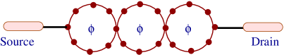
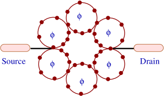
This section follows the theoretical formulation to study electron transport in an array of mesoscopic rings. The rings are coupled to each other through a single lattice site in such a way that both the upper and lower arms of each ring contains equal number of lattice sites. This configuration is the so-called symmetric configuration. The rings are arranged in two different ways, series and parallel, those are schematically presented in Figs. 1 and 2, respectively. Each ring in the array is subjected to an AB flux (measured in unit of (), the elementary flux-quantum) and the array is coupled to two semi-infinite D metallic electrodes, namely, source and drain.
To find the conductance () of the system, we use the Landauer conductance formula, where is expressed in terms of the transmission probability () of an electron as [33],
| (1) |
This relation is valid only for low temperatures and bias voltages. In
terms of the Green’s function of the array, transmission probability can be expressed like [33, 34],
| (2) |
where, and are the retarded and advanced Green’s functions of the array, respectively. Here, and are the broadening matrices representing the couplings of the array to the source and drain, respectively.
Now, the Green’s function for the whole system i.e., array and the electrodes, is defined as,
| (3) |
where, is the energy of the source electrons and is the Hamiltonian of the entire system which is of infinite dimension.
To evaluate this Green’s function, we require to calculate the inverse of an infinite dimensional matrix corresponding to the system consisting of a finite size array and the two semi-infinite electrodes, which is really a difficult task. The full Hamiltonian can be partitioned into sub-matrices corresponding to the individual parts of the system like,
| (4) | |||||
where, , and correspond to the Hamiltonians of the array, source and drain, respectively. and represent source-to-array and array-to-drain coupling, respectively. Within the framework of non-interacting electron picture, the tight-binding Hamiltonian of the array can be expressed in the form,
| (5) |
where, is the phase factor due the flux threaded by individual rings and is the total number of sites in each ring. Here, is the nearest-neighbor hopping integral, is the on-site energy and is the creation (annihilation) operator of an electron at the site . A similar kind of tight-binding Hamiltonian is also used, except the phase factor , to illustrate the side attached D perfect electrodes where the Hamiltonian is parametrized by constant on-site potential energy and nearest-neighbor hopping integral . Like the Hamiltonian, Green’s function can also be partitioned into sub-matrices and the effective Green’s function for the array is written as [33, 34],
| (6) |
where, and are the self-energies due to the coupling of the rings to the source and drain, respectively.
The broadening matrices and , in Eq. 2, are defined as the difference between the retarded and advanced self-energies of the electrodes. Explicitly, one can write,
| (7) |
and the self-energies can be expressed as [33],
| (8) |
where, the real parts () correspond to the shift of the energy levels of the array and the imaginary parts () represent the broadening of these energy levels. We do our calculations only at absolute zero temperature. But all these results are also valid at low temperatures for which is much smaller than the average spacing of the energy levels. Using Eq. 8, the broadening matrices can now be written as,
| (9) |
To evaluate the current passing through the array, we use the relation [33],
| (10) |
where, gives the Fermi distribution function with the electrochemical potential . is the applied bias voltage. Here, we assume that the entire voltage is dropped across the conductor-electrode interfaces, and, this assumption does not affect significantly the current-voltage characteristics in such a small array [35]. Throughout the calculation, we choose the units where and set the Fermi energy at .
3 Numerical results and discussion
3.1 Conductance-energy characteristics
In order to illustrate the results, we begin our discussion by mentioning the values of the different parameters used for the numerical calculations. In the ring, the site energy is fixed to and the nearest-neighbor hopping integral is set to . While, for the side-attached electrodes the on-site energy () and the nearest-neighbor hopping strength () are chosen as and , respectively. Throughout our study, we narrate all the essential features of electron transport in the two different regimes depending on the strength of the coupling of the ring to the source and drain. One is the weak-coupling regime defined by the condition . For this regime we choose . Other one is the strong-coupling regime defined by the relation . In this particular limit, we set the values of the parameters as . Here, and describe the coupling strengths of the ring to the source and drain, respectively. In addition to these, we also introduce two other parameters and to describe the size of the array, where they correspond to the ring size and total number of rings in the array, respectively.
To explore the basic mechanisms of electron transport in an array of
mesoscopic rings, we start with the results for a single ring () and then two rings () which are directly coupled to each other.
As illustrative examples, in Fig. 3 we plot the conductance as a function of injecting electron energy for a symmetrically connected mesoscopic ring, where (a) and (b) correspond to the results for the weak- and strong-coupling limits, respectively. Here we fix (total number of atomic sites in the ring, where the upper and lower arms contain atomic sites). All these results are calculated in the absence of AB flux . From the - spectra it is observed that, in the case of weak-coupling limit, conductance exhibits sharp resonant peaks for some particular energies, while it () disappears for the other energies. Thus, a fine tuning in the energy scale is required to get electron conduction across the ring. At resonances, conductance reaches the value , and accordingly, the transmission
probability approaches to unity, since the equation is satisfied from the Landauer conductance formula (see Eq. 1 with in our present formulation). All these resonant peaks are associated with the energy eigenvalues of the ring, and therefore, we can predict that the conductance spectrum manifests itself the fingerprint of the electronic structure of the ring. The situation becomes quite interesting as long as the coupling strength of the ring to the side attached electrodes is increased. In the limit of strong-coupling, all the resonant peaks get substantial widths compared to the weak-coupling case. The contribution to the broadening of the resonant peaks in this strong-coupling limit comes from the imaginary parts of the self-energies and [33]. Hence, by tuning the coupling strength, we can get the electron transmission across the ring for the wider range of energies which provides an important signature in the study of current-voltage (-) characteristics.
To emphasize the effect of AB flux on electron transport through such a ring, now we describe the results presented in Fig. 4. The results are computed for the same ring i.e., , considering , where (a) and (b) correspond to the weak- and strong-coupling cases, respectively. The effects of coupling on the resonant widths become exactly identical as in Fig. 3. But, quite interestingly, we observe that a global gap in the conductance spectrum appears across the energy as long as the flux is applied in the ring. This feature is clearly noticed by comparing the results plotted in Figs. 3 and 4. It is also verified that the gap across the energy increases gradually with the increase in , and at the typical flux , conductance exactly vanishes for the entire energy range [31, 32]. This vanishing behavior of the transmission probability at for a symmetrically connected ring, where the upper and lower arms are identical in nature, can be obtained very easily by a simple mathematical calculation as follows. For a symmetrically connected ring, the wave functions passing through the upper and lower arms of the ring are given by,
| (11) |
where, and are used to indicate the two different paths of electron propagation along the two arms of the ring. denotes the wave function in absence of magnetic flux and it is same for both upper and lower arms as the ring is symmetrically coupled to the electrodes. is the vector potential associated with the
magnetic field by the relation . Hence the probability amplitude of finding the electron passing through the ring can be calculated as,
| (12) |
where, is the flux enclosed by the ring. From Eq. 12 it is clearly observed that at the transmission probability of an electron through a symmetrically connected ring drops exactly to zero.
Now we study the conductance-energy characteristics for an array of two rings () having sites in each arm of the individual rings. In Fig. 5 we show the results for , while for the results are given in Fig. 6. Both for the weak- and strong-coupling limits we get exactly similar features of resonant peaks i.e., sharp in weak-coupling regime and broadened in strong-coupling regime, as presented in Figs. 3 and 4. Also, a finite gap across the energy appears
for any non-zero value of (for instance see Fig. 6). The only difference is that for such a two ring system number of resonant peaks, associated with the energy eigenvalues, in the conductance spectra gets increased compared to the one ring system. Apart from these features, from Figs. 5 and 6 we see that for some specific energy values resonances are of Fano type, where a sharp peak followed by a sharp deep is observed. With the increase of ring-to-electrode coupling strength, positions of these peaks and deeps and also their heights are unchanged. Only the widths get broadened with the increase of coupling strength. This behavior is quite different from the other resonant peaks where a sharp peak is not followed by a sharp deep.
Following the above conductance-energy characteristics of one and two
ring systems, now we focus our study on larger ring systems where the rings are arrayed both in series and parallel configurations to illustrate the effect of quantum interference on electron transport.
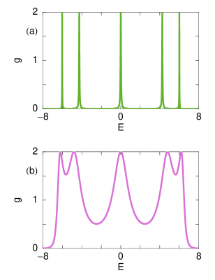
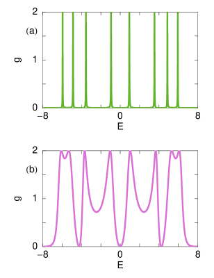
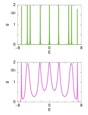
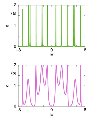
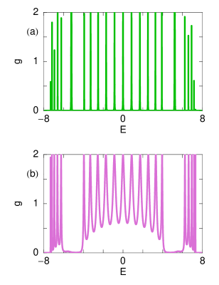
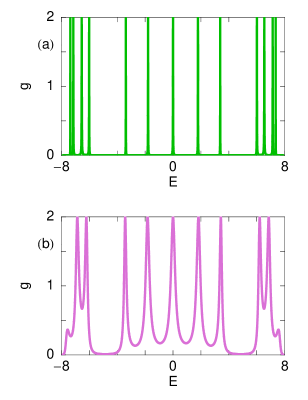
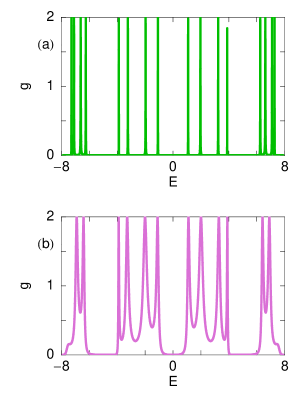
As representative examples, in Fig. 7 we plot the conductance-energy characteristics for an array of mesoscopic rings, where the rings are arranged in series configuration. The results are depicted for the array with and (upper and lower arms of each ring have atomic sites) in the absence of , where (a) and (b) correspond to the weak- and strong-coupling cases, respectively. For the same array, we display the results in Fig. 8, considering . On the other hand, the variation of conductance as a function of energy in the absence of for an array of rings, arranged in parallel configuration, is given in Fig. 9, where (a) and (b) represent
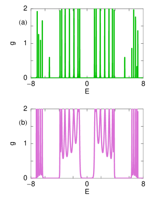
the identical meaning as in Fig. 7. Here we fix ( rings in each branch) and (upper and lower arms of each ring contain atomic sites). Both for the two different coupling limits, the nature of the resonant peaks is exactly identical as studied earlier (Figs. 3 and 4). Comparing the results presented in Figs. 7 and 9, we notice that in the parallel configuration of the rings, several resonant peaks disappear compared to their (rings) series configuration. This is solely due to the effect of quantum interference among the electronic waves passing through different arms of the rings and it provides an interesting feature in electron transport which can be much more clearly explained from our current-voltage characteristics (in sub-section ). In the same footing, as above, in Fig. 10 we plot the - characteristics for the same array ( and ) in the presence of (), where different curves represent the identical meaning as in Fig. 9. Similar to the case of , the
number of resonant peaks in the parallel configuration also decreases compared to the series configuration (Fig. 8) in the presence of . Thus, it is manifested that the number of resonant peaks in parallel configuration is always reduced than the series configuration irrespective of threaded by the rings. In Fig. 2, the rings are arranged in parallel configuration where each ring is penetrated by an AB flux . In such an arrangement a bigger loop is formed where we do not apply any magnetic flux for our present discussion. We can also apply a magnetic flux through this bigger loop and in that case an electron experiences two magnetic phases during the propagation through upper and lower arms of the rings. Even in that case i.e., in the presence of two fluxes, the number of resonant resonant peaks in parallel configuration is much smaller compared to the series one. Thus in short we can say that, appearance
of more resonant peaks in series configuration than the parallel one is valid for the cases when (i) there is no flux through individual rings as well as in bigger loop, (ii) in presence of AB fluxes in the smaller rings only, but, not in the bigger ring and (iii) in presence of AB fluxes through identical rings as well as in bigger ring. All these features can also be justified through proper experimental arrangement.
3.2 Current-voltage characteristics
All the basic features of electron transport obtained from conductance versus energy spectra can be explained in a better way through the current-voltage (-) characteristics. The current across the array is determined by integrating over the transmission curve according to Eq. 10 which is not restricted in the linear response regime, but it is of great significance in determining the shape of the full current-voltage characteristics. As representative examples, in Fig. 11 we display
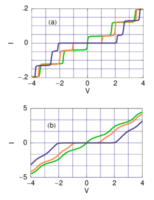
the current-voltage (-) characteristics for an array of symmetrically connected mesoscopic rings in the series configuration, where (a) and (b) correspond to the results for the weak- and strong ring-to-electrode coupling limits, respectively. The currents are evaluated for an array considering and , where the green, orange and blue lines correspond to the currents for , and , respectively. From the results it is observed that, in the case of weak-coupling, current exhibits staircase-like structure with sharp steps as a function of the applied bias voltage. This is due to the presence of fine resonant peaks in the conductance spectra, as the current is obtained from integration method over transmission function . With the increase
in applied bias voltage , the difference in chemical potentials of the two electrodes increases, allowing more number of energy levels to fall in that range, and therefore, more number of energy channels are accessible to the injected electrons to pass through the array from the source to drain. Incorporation of a single discrete energy level i.e., a discrete quantized conduction channel, between the range provides a jump in the - characteristics. In addition to this step-like feature, we also observe that in the absence of , current shows non-zero value i.e., electron is allowed to pass through the array as long as the bias voltage is switched on (see the green curve). While, in the presence of , the conduction of an electron is started beyond some finite value of the bias voltage, the so-called threshold voltage (see the orange and blue lines), which is clear from the - spectrum shown in Fig. 8(a). Thus, by changing the value of , can be regulated in a controlled way. This behavior may be useful in designing nano-scale electronic devices. The nature of the - spectra changes significantly in the case of strong-coupling (Fig. 11(b)). Here, the current varies almost continuously as a function of the bias voltage and achieves much higher current amplitude, even an order of magnitude, compared to the weak-coupling case. Therefore, we can emphasize that for a fixed bias voltage , one can enhance the current amplitude through the bridge system by tuning the ring-to-electrode coupling strength.
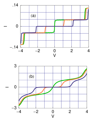
At the end, we describe the effect of interface geometry on the behavior of - characteristics. The results are plotted in Fig. 12, where (a) and (b) correspond to the identical meaning as in Fig. 11. In this parallel configuration, both for the weak- and strong-coupling regimes, behavior of the current i.e., step-like and continuous nature, is exactly similar to that as discussed in the case of series configuration. But, the key observation is that, for a fixed ring-electrode coupling strength and applied bias voltage, the current amplitude obtained in the parallel configuration is much smaller compared to that in the series configuration. This anomalous behavior is completely different from the traditional resistors where the current amplitude obtained in the case of parallel arrangement is much higher than that in series configuration. All these features of electron transport may provide some physical insight to study transport properties in array-like geometries.
4 Concluding remarks
To conclude, we have addressed the electronic transport properties in an array of mesoscopic rings, where each ring is threaded by an AB flux . Both the series and parallel configurations of the rings are considered to reveal the quantum interference effect on electron transport. A parametric approach based on the tight-binding framework is given where all the calculations are done through the Green’s function formalism. Our exact numerical calculations describe conductance-energy and current-voltage characteristics in aspects of (a) ring-to-electrode coupling strength, (b) ring-electrode interface geometry and (c) magnetic flux. Most significantly we predict that, in a series configuration of mesoscopic rings the typical current amplitude is much higher compared to their parallel configuration. This phenomenon is completely different from the traditional one. Here, we have presented our results only for the array of symmetrically connected mesoscopic rings. All these features are also valid for an array where the rings are coupled asymmetrically to each other and due to the obvious reason we do not plot those results further. Our exact analysis may provide some important signatures to study electron transport in nano-scale systems.
Throughout our work, we have explored the conductance-energy and current-voltage characteristics for an array of mesoscopic rings each having atomic sites. In our model calculations, these typical numbers are chosen only for the sake of simplicity. Though the results presented here change numerically with the ring size and total number of rings, but all the basic features remain exactly invariant. To be more specific, it is important to note that, in real situation the experimentally achievable rings have typical diameters within the range - m. In such a small ring, a high magnetic field is required to produce a quantum flux. To overcome this situation, Hod et al. have studied extensively and proposed how to construct nanometer scale devices, based on Aharonov-Bohm interferometry, those can be operated in moderate magnetic fields [36, 37, 38, 39]. In addition, it is also important to note that here we have done all the numerical calculations for some specific values of the parameters. One can also compute these results for some other typical values of the parameters. In that case only the numerical values will be changed, but the basic characteristics remain unaltered.
In the present paper we have done all the calculations by ignoring the effects of the temperature, disorder, electron-electron correlation, etc. The effect of the temperature has already been reported earlier, and, it has been examined that the presented results will not change significantly even at finite (low) temperature, since the broadening of the energy levels of the ring system due to its coupling to the electrodes will be much larger than that of the thermal broadening. In presence of disorder, scattering process appears in the arms of the rings that can influence the electronic phases, and accordingly, the quantum interference effect is disturbed. All the above pictures are also valid if electron-electron interaction is taken into account. In presence of electronic correlation, the on-site Coulomb repulsive energy gives a renormalization of the site energies [40]. Depending on the strength of the nearest-neighbor hopping integral () compared to the on-site Coulomb interaction () different regimes appear. For the case , the resonances and anti-resonances would split into two distinct narrow bands separated by the on-site Coulomb energy. On the other hand, for the case where , the resonances and anti-resonances would occur in pairs. In a recent work, Montambaux et al. [41] have studied elaborately the effect of electron-electron correlation on electron transport for some arrays of connected mesoscopic metallic rings. In this work, they have studied how at low temperatures, decoherence is limited by electron-electron interaction. Finally, we would like to say that we need further study in such systems by incorporating all these effects.
References
- [1] Y. Imry, Introduction to Mesoscopic Physics, Oxford University Press, Oxford (2002).
- [2] Y. Imry and R. Landauer, Rev. Mod. Phys. 71, S306 (1999).
- [3] J. Xia and S. Li, Phys. Rev. B 66, 035311 (2002).
- [4] P. Cedraschi and M. Büttiker, Phys. Rev. B 63, 165312 (2001).
- [5] S. K. Maiti, Physica E 36, 199 (2007).
- [6] B. Molnar, P. Vasilopoulos and F. M. Peeters, Phys. Rev. B 72, 075330 (2005).
- [7] O. Kalman, P. Földi, M. G. Benedict and F. M. Peeters, Phys. Rev. B 78, 125306 (2008).
- [8] T. Bergsen, T. Kobayashi, Y. Sekine and J. Nitta, Phys. Rev. Lett. 97, 196803 (2006).
- [9] P. Földi, O. Kalman, M. G. Benedict and F. M. Peeters, Nano Lett. 8, 2556 (2008).
- [10] G. Montambeux, H. Bouchiat, D. Sigeti and R. Friesner, Phys. Rev. B 42, 7647 (1990).
- [11] H. Bouchiat, G. Montambeux and D. Sigeti, Phys. Rev. B 44, 1682 (1991).
- [12] S. K. Maiti, Solid State Phenomena 155, 87 (2009).
- [13] L. K. Castelano, G.-Q. Hai, B. Partoens and F. M. Peeters, Phys. Rev. B 78, 195315 (2008).
- [14] D. Mailly, C. Chapelier and A. Benoit, Phys. Rev. Lett. 70, 2020 (1993).
- [15] E. M. Q. Jariwala, P. Mohanty, M. B. Ketchen and R. A. Webb, Phys. Rev. Lett. 86, 1594 (2001).
- [16] L. P. Levy, G. Dolan, J. Dunsmuir and H. Bouchiat, Phys. Rev. Lett. 64, 2074 (1990).
- [17] K. L. Hobbs, P. R. Larson, G. D. Lian, J. C. Keay and M. B. Johnson, Nano Lett. 4, 167 (2004).
- [18] D. H. Pearson, R. J. Tonucci, K. M. Bussmann and E. A. Bolden, Adv. Mater. 11, 769 (1999).
- [19] F. Yan and W. A. Geodel, Nano Lett. 4, 1193 (2004).
- [20] A. Chakrabarti, R. A. Römer and M. Schreiber, Phys. Rev. B 68, 195417 (2003).
- [21] W. Y. Cui, S. Z. Wu, G. Jin, X. Zhao and Y. Q. Ma, Eur. Phys. J. B 59, 47 (2007).
- [22] Y. Liu, H. Wang, Z. Zhang and X. Fu, Phys. Rev. B 53, 6943 (1996).
- [23] A. Aviram and M. Ratner, Chem. Phys. Lett. 29, 277 (1974).
- [24] Y. Oreg and O. Entin-Wohlman, Phys. Rev. B 46, 2393 (1992).
- [25] Y. Oreg, New J. Phys. 9, 122 (2007).
- [26] Y. Meir and N. S. Wingreen, Phys. Rev. Lett. 68, 2512 (1992).
- [27] Y. Meir, N. S. Wingreen and P. A. Lee, Phys. Rev. Lett. 66, 3048 (1991).
- [28] R. Baer and D. Neuhauser, Chem. Phys. 281, 353 (2002).
- [29] R. Baer and D. Neuhauser, J. Am. Chem. Soc. 124, 4200 (2002).
- [30] D. Walter, D. Neuhauser and R. Baer, Chem. Phys. 299, 139 (2004).
- [31] S. K. Maiti, Phys. Lett. A 373, 4470 (2009).
- [32] S. K. Maiti, J. Phys. Soc. Jpn. 78, 114602 (2009).
- [33] S. Datta, Electronic Transport in Mesoscopic Systems, Cambridge University Press, Cambridge (1997).
- [34] S. Datta, Quantum Transport: Atom to Transistor, Cambridge University Press, Cambridge (2005).
- [35] W. Tian, S. Datta, S. Hong, R. Reifenberger, J. I. Henderson and C. I. Kubiak, J. Chem. Phys. 109, 2874 (1998).
- [36] O. Hod, R. Baer and E. Rabani, J. Phys. Chem. B 108, 14807 (2004).
- [37] O. Hod, R. Baer and E. Rabani, J. Phys.: Condens. Matter 20, 383201 (2008).
- [38] O. Hod, R. Baer and E. Rabani, J. Am. Chem. Soc. 127, 1648 (2005).
- [39] O. Hod, E. Rabani and R. Baer, Acc. Chem. Res. 39, 109 (2006).
- [40] V. Mujika, A. Nitzan, S. Datta, M. A. Ratner and C. P. Kubiak, J. Phys. Chem. B 107, 91 (2003).
- [41] C. Texier, P. Delplace and G. Montambaux, arXiv:0907.3133v1.