Quantum effects in linear and non-linear transport of T-shaped ballistic junction
Abstract
We report low-temperature transport measurements of three-terminal T-shaped device patterned from GaAs/AlxGa1-xAs heterostructure. We demonstrate the mode branching and bend resistance effects predicted by numerical modeling for linear conductance data. We show also that the backscattering at the junction area depends on the wave function parity. We find evidence that in a non-linear transport regime the voltage of floating electrode always increases as a function of push-pull polarization. Such anomalous effect occurs for the symmetric device, provided the applied voltage is less than the Fermi energy in equilibrium.
pacs:
73.21.Nm, 73.23.Ad, 85.35.DsRecently, nanotechnology advances have led to a growing interest in electrical transport properties of the so-called three-terminal ballistic junctions (TBJs). As the name indicates, such structures consist of three quantum wires connected via a ballistic cavity to form a Y-shaped or T-shaped current splitter. One motivation is that in principle such systems can operate at high speed with a very low power consumption. Therefore, interesting and unexpected nonlinear transport characteristics of TBJs are intensively investigated due to possible applications as high frequency devices or logic circuitsXu (2005); Worschech et al. (2005).
Another reason for the increased number of studies devoted to TBJs are quantum mechanical aspects of carrier scattering, which dominate at low temperatures in the linear transport regime. This applies especially to T-shaped splitters. For example, it is expected that a T-branch switch, made of materials with a significant spin-orbit interactions, can act as an effective spin polarizer Kiselev and Kim (2001). Also, for such geometry an ideal splitting of electrons from a Cooper pair is expected, provided the lower part of the letter T is made of a superconducting material Bednorz et al. (2009). Both effects rely very strongly on the perfect shape of the devices and high enough transparency of individual wires. Unfortunately, experimental data available for the lithographically perfect T-branch junctions are limited mostly to a non-linear transport regime Wallin et al. (2006). Quantum linear transport is usually studied for less symmetric structures, typically consisting of short point contact attached to a side wall of a wider channel Usuki et al. (1995).
In this work we report on fabrication and low temperature transport measurements of T-shaped three-terminal devices, for which we take a special care to preserve the perfect symmetry and reduce the geometrical disorder. By comparing our data to conductance modeling by the recursive Green-function method, we find out that quantum effects dominate up to source-drain voltages equal to the Fermi energy. In particular, we show that the non-linear response of symmetric TBJ behaves in a non-classical way and is highly tunable with carrier density.
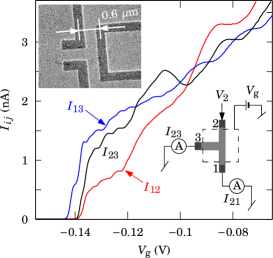
The three-terminal ballistic junctions are made of a GaAs/AlGaAs:Si heterostructure with electron concentration cm-2 and carrier mobility cm2/Vs. The interconnected wires of equal length m and lithographic width m are patterned by e-beam lithography and shallow-etching techniques to form a T-shaped nanojunction (see inset to Fig.1). The physical width of all branches is simultaneously controlled by means of a top metal gate which is evaporated over the entire structure. The differential conductances have been measured in a He-3/He-4 dilution refrigerator, by employing a standard low-frequency lock-in technique. We have also studied non-linear transport in the typical for TBJs, so-called push-pull bias regime, when equal but opposite in sign voltages are simultaneously applied to the opposite input contacts.
The application of a metal gate over the active region of the device helps to symmetrize transmission coefficients by smoothing the confinement potential Liu et al. (1994). Nevertheless, even a perfectly shaped and gated junction may remain disordered at low electron densities, when screening effects are weak. Figure 1 shows linear currents flowing from each of three terminals for negative gate voltages close to the threshold regime. The data indicate clearly that there is a weak asymmetry between contacts – channels open at slightly different Additionally, small reproducible wiggles are visible above threshold voltage. All investigated structures show similar behavior and we attribute it to the presence of quasi-localized states, formed in the central part of the device. In this paper we present data for the sample which has a lowest disorder and highest degree of symmetry.
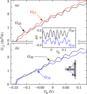
Although channel opens last, at higher electron densities is larger than and , as predicted by Baranger Baranger (1990) for the ideal T-shaped quantum splitter. Figure 2 presents the conductances as a function of gate voltage up to V. For V the regular oscillations corresponding to the successive population of electric sub-bands in each of the three terminals are visible. Since magnetic field is zero, we expect and this is indeed observed in the experiment. For example, curves and are almost identical. Larger differences are noticed for and curves which should be equal for the perfectly shaped device. Relevant data are presented in the inset to Fig.2 where oscillating parts of and are compared. On average is smaller and oscillate less regularly than . Nevertheless, maxima and minima on both curves are close to each other and for V they oscillate exactly in phase. It means that starting from a disordered structure at the threshold voltage, for the device becomes more symmetrical and experimental data can be compared with the theory of ballistic transport.
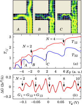
We model TBJ by three semi-infinite strips of “atoms” and the square coupling region. Calculations have been performed at temperature , using a tight-binding approach and a recursive Green functions technique Bułka and Tagliacozzo (2009). To determine a local current intensity inside the junction we have incorporated parts of each wire to the coupling region and used a newly developed, so-called knitting algorithm Kazymyrenko and Waintal (2008). Results of this modeling are presented in Fig. 3(a). Transmission coefficients between -th and -th electrode are calculated for disorder free and symmetric device with rounded corners in the coupling region. Note that the value of increases almost monotonically as a function of energy, whereas oscillates strongly. This is the co-called bend resistance effect. reaches maximum when the upper, just populated sub-band, is almost fully transmitted to the terminal (see intensity plot ). For higher kinetic energies, however, coupling becomes weaker and as a result decreases, leading to the non-monotonic behavior as a function of Fermi energy .
Presented calculations are consistent with the experimental data obtained at electron densities high enough. For the curve is similar to and rather smooth as compared to , which (like ) shows deeper minima due to the bend resistance effect (see Fig. 2). Note also, that calculated energy dependence of transmission coefficients differ for odd and even channel numbers. For example, the backscattering for and channels is stronger, as indicated with arrows in Fig. 3. This effect was already predicted for a perfect T coupler Baranger (1990) and is apparently enhanced by the rounding of the “corners” in a junction area. For even parity modes electron has high probability density at the center of the device and therefore is more likely transmitted (to see this compare density plots and ). We believe that such conductance dependence on wave function parity is also observed in the experiment. It is especially well resolved for the total conductance . Relevant data are presented in Fig. 3(b).
Next we consider the measurement scheme where stub terminal () acts as a floating voltage probe (). For a classical device we have . This simple formula should be modified for ballistic transport, where it takes form with for simplicity. If then classical result is recovered.
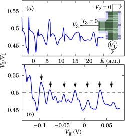
Conductance data shown in Fig. 2(b) indicate that on average is smaller than . Therefore, to imitate the real sample, we rounded the junction “corners” of a model device in such a way that . The shape of the coupling area and results of calculations are shown in Fig. 4(a). Ratio is on average below but oscillates as energy increases. Very similar dependence is observed in the experiment. The measured value of ratio reaches maximum, each time a new one-dimensional level becomes occupied. Interestingly, theory also predicts the occurrence of additional asymmetric and very narrow resonances when a new conduction channel opens to transport in stub terminal. They are probably related to the so-called Wigner singularities, which exist when the energies of quantized levels in a side probe differ from those in the rest of the deviceBułka and Tagliacozzo (2009). Similar features are also visible in the experiment, especially for , but their possible connection to Wigner resonances requires further studies.
Now let us turn to the non-linear transport regime where the probabilities of transmission from input terminals to a floating contact may differ, even for a perfect device. In such case, when is large enough and positive, then is less then . Equivalently, if and (push-pull bias regime) then is always negative, as it was predicted in Xu (2001) and then proved experimentally Shorubalko et al. (2001). Using the quantum scattering approach Csontos and Xu Csontos and Xu (2003) extended the calculation range to a low temperature regime. They showed that may be also positive, provided and . To our knowledge, however, the predictions of Ref. Csontos and Xu (2003) have not been confirmed experimentally.
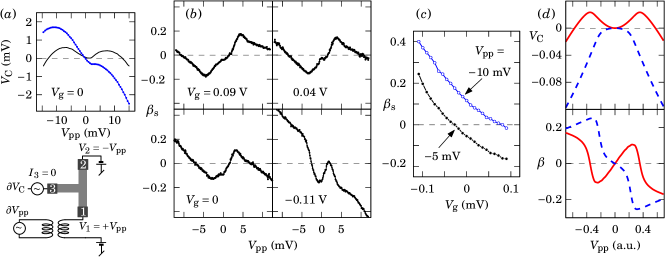
Figure 5(a) shows measurement schematics and corresponding data obtained when mV. is not a symmetric function of , yet above a certain threshold, data — as expected — bend towards negative values of . Such behavior is often observed in experiments Shorubalko et al. (2001) because due to imperfections which are always present in the real devices. Apart from such asymmetry, however, data reported here behave in an anomalous way. When a linear trend has been removed, first increases with , and then goes down reaching maximum at mV. To investigate this effect in more detail we have used a modulation method to measure the switching parameter directly with a better voltage resolution. Figure 5(a) explains the measurement idea and Fig. 5(b) shows values of parameter as a function of for a different gate voltages. Here is the mean value of switching parameter calculated at each for mV. Subtracting is equivalent to removing a linear trend from the dc data and therefore reduces the influence of the vs asymmetry.
To compare the experimental findings with theory we calculated and for an ideal T-shaped junction from the energy dependence of a transmission coefficients. Results are consistent with the explanation of Xu Xu (2001), as it follows from Fig. 5(d). If then increases with and has a positive slope in this voltage range. When stub voltage is negative and switching parameter behaves “normally”. Interestingly, when experimental data are compared to linear conductance no such correlation can be found. For example at , , and V, derivative is negative, positive and approximately zero, but switching parameter does not change its shape and sign as would be expected from modeling. Results indicate that an anomalous data range, where has a positive slope, always exists — only its width decreases with . This fact can be used to tune switching parameter with the gate voltage. Figure 5(c) shows as a function of for the two values of . Remarkably, not only amplitude but also the sign of can be changed. We conclude that the behavior of in Fig. 5 cannot be explained by a single particle transmission approach. Probably, as suggested in Büttiker and Sánchez (2003), the non-linear transport regime requires a self-consistent calculations.
In summary, we have shown that linear transport in T-shaped ballistic junction can be successfully described by quantum scattering effects and weak disorder in a cavity area. We have shown for the first time, that stub voltage can increase as a function of push-pull polarization in a non-linear transport regime, however, the energy dependence of such non-equilibrium effect is inconsistent with the standard single-particle picture of electron transmission. Nevertheless, novel applications of symmetric TBJ structure, for example as the component of a multilogic device, are still possible.
Acknowledgements.
This work was funded by grant No. 107/ESF/2006 and MNiSW projects N202/103936 and N202/229437.References
- Xu (2005) H. Q. Xu, Nat. Mater. 4, 649 (2005).
- Worschech et al. (2005) L. Worschech, D. Hartmann, S. Reitzenstein, and A. Forchel, in J. Phys.: Condens. Matter 17, R775 (2005).
- Kiselev and Kim (2001) A. A. Kiselev and K. W. Kim, Appl. Phys. Lett. 78, 775 (2001).
- Bednorz et al. (2009) A. Bednorz, J. Tworzydło, J. Wróbel, and T. Dietl, Phys. Rev. B 79, 245408 (2009).
- Wallin et al. (2006) D. Wallin, I. Shorubalko, H. Q. Xu, and A. Cappy, Appl. Phys. Lett. 89, 092124 (2006); D. Spanheimer, C. R. Muller, J. Heinrich, S. Hofling, L. Worschech, and A. Forchel, Appl. Phys. Lett. 95, 103502 (2009).
- Usuki et al. (1995) T. Usuki, M. Saito, M. Takatsu, R. A. Kiehl, and N. Yokoyama, Phys. Rev. B 52, 8244 (1995); A. Ramamoorthy, J. P. Bird, and J. L. Reno, J. Phys.: Condens. Matter 19, 276205 (2007).
- Liu et al. (1994) J. Liu, W. X. Gao, K. Ismail, K. Y. Lee, J. M. Hong, and S. Washburn, Phys. Rev. B 50, 17383 (1994).
- Baranger (1990) H. U. Baranger, Phys. Rev. B 42, 11479 (1990).
- Bułka and Tagliacozzo (2009) B. R. Bułka and A. Tagliacozzo, Phys. Rev. B 79, 075436 (2009), and references therein.
- Kazymyrenko and Waintal (2008) K. Kazymyrenko and X. Waintal, Phys. Rev. B 77, 115119 (2008).
- Xu (2001) H. Q. Xu, Applied Physics Letters 78, 2064 (2001).
- Shorubalko et al. (2001) I. Shorubalko, H. Q. Xu, I. Maximov, P. Omling, L. Samuelson, and W. Seifert, Applied Physics Letters 79, 1384 (2001); L. Worschech, H. Q. Xu, A. Forchel, and L. Samuelson, Appl. Phys. Lett. 79, 3287 (2001).
- Csontos and Xu (2003) D. Csontos and H. Q. Xu, Phys. Rev. B 67, 235322 (2003).
- Büttiker and Sánchez (2003) M. Büttiker and D. Sánchez, Phys. Rev. Lett. 90, 119701 (2003).