Fabrication of a planar micro Penning trap and numerical investigations of versatile ion positioning protocols
Abstract
We describe a versatile planar Penning trap structure, which allows to dynamically modify the trapping configuration almost arbitrarily. The trap consists of 37 hexagonal electrodes, each with a circumcirle-diameter of 300 m, fabricated in a gold-on-sapphire lithographic technique. Every hexagon can be addressed individually, thus shaping the electric potential. The fabrication of such a device with clean room methods is demonstrated. We illustrate the variability of the device by a detailed numerical simulation of a lateral and a vertical transport and we simulate trapping in racetrack and artificial crystal configurations. The trap may be used for ions or electrons, as a versatile container for quantum optics and quantum information experiments.
pacs:
37.10.Ty, 03.67.Lx1 Introduction
Trapped ions have been an important workhorse for quantum information research, even though research has been mostly limited to one dimensional arrangements of ion crystals in radio frequency Paul traps [1, 2]. Planar Paul traps have shown their advantages for scalable micro fabricated devices [3, 4, 5, 6, 7, 8], even for trapping cold molecules [9]. However a two-dimensional arrangement of ions [10] still needs to be shown. Inspired by experiments with large, rotating planar ion crystals in Penning traps [11], as well as single ions [12] or electrons [13, 14], novel designs for Penning traps have been proposed [15, 16, 17]. As an advantage [18], Penning traps operate with only static electric and magnetic fields, thus noise and heating issues as observed for radio frequency ion traps [19] are expected to be largely suppressed. The AC drive of Paul traps, with frequencies from 1 to 100 MHz, and with peak-to-peak voltages in the range of a few 100 V constitutes a considerable source of noise, which affects and heats the trapped particles via free charges and surface patches. The Penning trap, however, even when ions are trapped in the vicinity of slightly contaminated surfaces, still is expected to exhibit much better noise properties, as all fields including the patch fields are static.
The static magnetic field lifts the degeneracy of ground state spin states, allowing for a natural choice of qubit basis states. Currently, one of the most urgent unsolved scientific tasks in our field concerns building a scalable quantum information processing device. In this letter we show that novel planar and micro structured Penning traps allow for trapping various qubit configurations including two-dimensional ion crystals with well controlled interactions between individual qubits and with individual initialization and readout. Cluster state generation and quantum simulation are future applications of such tailored qubit arrays.
The paper first describes a pixel micro structure to generate the complex electric potential for the novel Penning trap. We briefly sketch the numerical method to calculate the potential landscape with the required high accuracy and optimize the control voltages for a selected set of qubit configurations and qubit operations. We estimate two-qubit spin-spin interactions [20, 21], which would lead either to a multi-qubit cluster state [22] or the realization of plaquette physics [23] in a rich, however well controlled quantum optical few-spin-system. In the last section we show the fabrication of such a device with state of the art clean room technology.
2 Versatile trapping configurations and numerical simulations
The genuine three dimensional Penning trap [44, 13, 14] is composed of a quadrupole electrical potential provided by a voltage applied between a ring electrode and two electrically isolated end cap electrodes of hyperbolic shape, and a superimposed constant magnetic field B0 in the direction of the -axis.
| (1) |
The characteristic dimension of the trap electrodes is denoted by . The electric field confines charged particles in the axial-direction (along the -axis) while the magnetic field prevents them from escaping in the radial direction . The motion in this potential consist of three harmonic quantum oscillations at the frequencies
| (2) | |||||
| (3) |
where is the free cyclotron frequency, 400 kHz/T in case of ions, which means that in typical experimental settings with singly charged ions [11, 12] one may reach a few MHz of cyclotron frequency. In the case of trapped electrons [13, 14, 24] the cyclotron frequency easily exceeds even 100 GHz. is called the reduced cyclotron frequency, the magnetron frequency, and the axial frequency. We note that in the radial direction the ion moves on a potential hill, making the magnetron motion metastable, where the energy of the magnetron motion decreases with increasing quantum number. Axialization, for example by using a rotating electric field (see sect. 2.1.1), excites the ion thereby moving it towards the center. The Penning trap stability condition (see, e.g., [44]) limits the maximum axial confinement frequency.
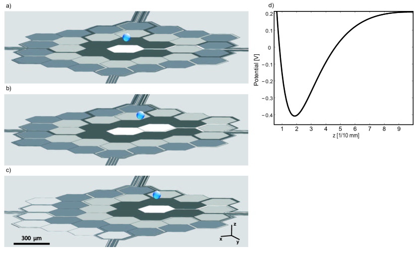
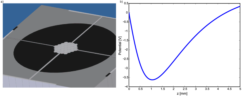
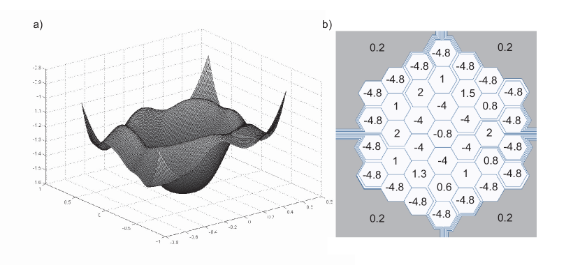
In our case the electric field is generated by surface electrodes in one plane [17] instead of the three dimensional ring structure, see Fig. 1. Apart from this construction feature, the motional degrees of freedom are similar to those in a three dimensional Penning trap. In a complex geometry such as our Pixel trap with a large number of different electrodes to control the confinement, see Fig. 1a, numerical simulations are used to find a set of voltages for specific tasks and configurations with a few ion qubits. For the shape of the control electrodes, we decided to use a hexagonal shape with a circumcircle diameter of 300m, which allows the forming of spherically symmetric potential field geometries.
In order to obtain accurate electrostatic potentials with minimum numerical noise for our geometry we apply the fast multipole method for the boundary element problem and calculate the potentials with the exact expressions[40]. Therefore a mesh of surface rectangles is placed on the surface geometry and the surface charges are then obtained in only steps. As opposed to finite elements or difference methods only surface elements have to be meshed. When the surface charges for the individual voltage configurations are calculated the potential at any point in space can be obtained by summing over the surface charges weighted by a distance dependent scaling function.
2.1 Single ion trapping
For an initial trapping of ions, one usually chooses a large trapping volume. To that end all control voltages of the pixels are set to 0 V while the outer four circular segments are at -10 V and the four outermost electrodes at +10 V. The resulting potential exhibits an axial frequency of 500 kHz and a depth of 3.5 eV, ideally suited for trapping, cooling and observing a large cloud, see Fig. 2.
Starting from this initial setting, the inner electrodes are employed for single ion trapping and we make use of the advanced configurations possible in a Pixel trap. Optimal potentials are obtained by applying regularization techniques [40]. If we supply the voltages V (white), V (black), V (light grey), V (dark grey), V (quartered ring, black), V (outside plane, grey), see figures 1a) and 2a), we would be able to reach a tight trap with an axial frequency of MHz and a trap depth of eV. The trap minimum is located at a distance of mm from the electrode surface, the anharmonicities are minimal and only lead to a broadening of the trap frequency well below a kHz for a particle as hot as K. We propose to load and laser-cool ions in the deep potential (see previous paragraph) and then alter the voltages to generate a harmonic well.
2.1.1 Transporting a single ion
Ions may be transported in the Pixel trap either (i) orthogonal to the plane of electrodes, a transversal transport, or (ii) in a lateral transport parallel to the trap electrode surface. In the case of (i) the pixels are arranged as rings on equal potential, such that the position of the minimum of the axial potential varies [25]. A possible application of a transversal transport would be the determination of motional heating and decoherence rates as a function of ion-surface distance, similar to attempts for dynamic Paul traps [26]. The lateral transport is sketched in Fig. 1 (a) to (c) (conceptually) as well as Fig. 3 (radial potentials). Starting out with a configuration that uses a single pixel as its center, we widen it up to an elongated center, including adjacent pixels, then we tilt the potential in the direction of the new center and finally finish with a single ion confinement at the displaced position. In our scheme, we intend to vary the electric field slowly, such that the much faster cyclotron orbiting can follow adiabatically. Alternatively, for other types of planar Penning traps, it has been proposed [27] to apply a pulsed electric transversal field for a non-adiabatic transport.
The ion is confined near the maximum of the radial electric potential as the magnetron oscillation corresponds to an inverted harmonic potential. Axialisation, an excitation of the ion’s magnetron frequency, centers it to . Experimentally, the outer four segments, see Fig. 2 may be employed to generate a rotating wall potential for this excitation [28].
2.2 Ring crystals and racetrack configuration
In a linear Paul trap, typically ions arrange as linear ion strings, while two- or three-dimensional arrangements of ions suffer from micro motion in the dynamical trapping field since the micro motion vanishes only along one line, where the RF field is zero [29, 30]. For crystal sizes on the order of m, this motion reaches amplitudes on the order of m. Here, a clear advantage of the purely static electric field of a Penning trap becomes evident, because in our geometry two-dimensional “artificial ion crystals” may be trapped by creating multiple trapping sites. The only relevant motion left in this case is the cyclotron motion, which in the case of an electron in a cryogenic trap (i.e. K, see [24]) would have an orbit-radius of nm and in the case of a laser-cooled Calcium ion (i.e. mK) a radius of nm111An ion at room-temperature would of course show a quite large cyclotron orbit of m.
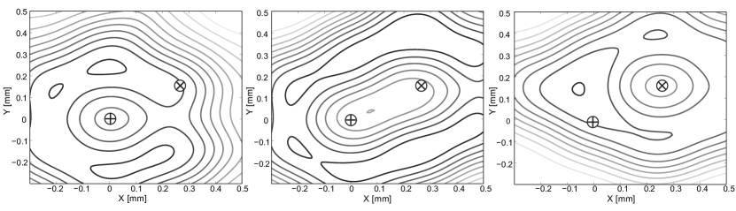
We highlight this with an arrangement of sites around a circle, trapping for example three ions in predefined places. One example of such an electrode configuration is shown in figure 4a. The potential in the xy-plane above such an electrode configuration is displayed in figure 4b with three trapping sites. The interest of the Pixel Penning trap is that various different kinds of such configurations may be converted into each other by a time-dependent addressing of the pixel electrodes.
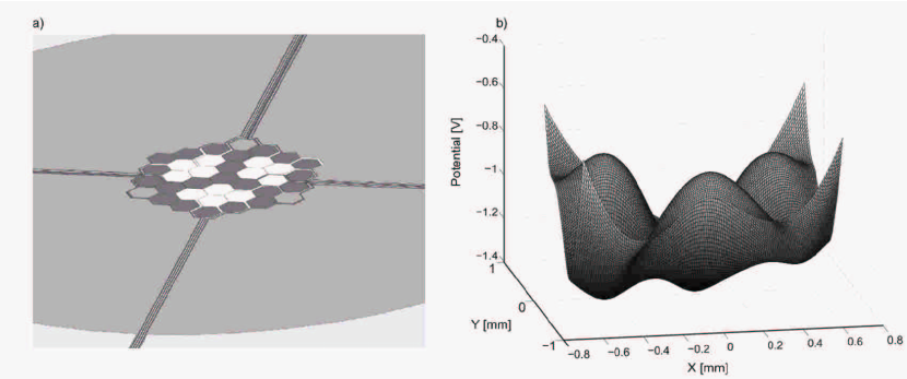
The colloquial term “racetrack” is commonly used for a configuration in which the trapping zone is in the form of a ring. Radio frequency ion traps have been used to hold linear crystals in a racetrack configuration [31], inspired by confined charged particles in accelerator rings. Magnetic traps with additional radio-frequency fields have been proposed for racetrack configurations for interferometric purposes [32]. Optical potentials for trapping neutral atoms [36, 37] are yet another option. Our Penning trap approach does not require any time dependent fields, advantageous with regard to heating and decoherence, and technically less demanding. In the Pixel Penning trap we may realize a 580 m diameter racetrack, see Fig. 5.
3 Fabrication of the Pixel trap
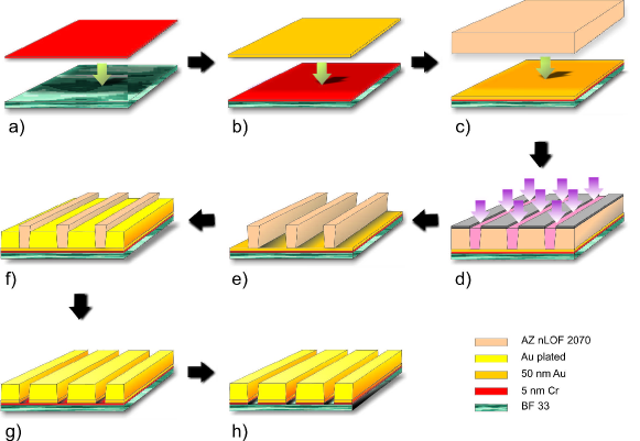
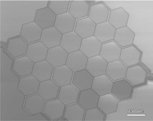
Starting with the CAD file of the trap design, we realize the fabrication of planar Penning traps by three-step clean room processing: photolithography, electroplating and etching. The fabrication is schematically presented in Fig. 6. A polished borosilicate glass wafer serves as substrate. We have achieved similar results with 2” sapphire wafers of thickness mm, which has the advantage of better heat conduction, even at cryogenic temperatures. In order to ensure proper adhesion of the Au electrodes to the substrate an adhesion promoter layer is mandatory. We use a 5 nm Cr layer deposited on the wafer via thermal evaporation. Furthermore, to enhance Au electrodeposition a 50 nm Au seed layer is also thermally deposited on top and a negative resist 222AZ® nLOF 2070 is added. Photolithography is then carried out. The mask resist lines which define the gaps between electrodes show a width of 4.0 m. Electrodes are grown up to 4.0 m in a Au plating bath 333mixture of Enthone GRC complex and Enthone microfab Au-100B. This means we achieve an aspect ratio of 1 between depth and width of the gaps between the electrodes, shielding inter-electrode insulating substrate gaps from the ion position. After electroplating the resist mask is stripped off. The Au seed layer is removed (using KI/I2 gold etchant) and a final Cr etching step is performed. Fig. 7 shows an Scanning Electron Microscopy micrograph of the inner center of the Pixel trap.
.
We dice the wafers and ball bond the chip electrodes to an 84-pin Kyocera chip carrier using 25 m Au wires. Under UHV conditions with we investigate the limit of the applied electric field by raising slowly the applied voltage. We observe a breakdown at approximately 180 V for 1.2 m to 720 V for 4.0 m gap width, respectively, far above the required trap voltages.
4 Outlook
As a next step, we plan experimental tests with single trapped 40Ca+ ions in the Pixel trap in order to particularly optimize the control of the transport processes [38, 39]. The Pixel trap opens a way to miniaturized Penning traps, and once the coherence properties have been tested with single ions close to surfaces, one might further reduce the spatial dimensions of the surface electrodes to about 10 m, including a dual layer technique [8]. In a planar arrangement of trapped atoms one may perform entanglement gate operations which are mediated by an inhomogenious magnetic field [20, 22]. The interaction Hamilton operator H denotes the coupling of two spins, where the strength of the coupling can be controlled by the distance of the atoms and the magnetic gradient field. With ion-ion distances of a few 10m, and realistic magnetic gradient fields of to T/m one will reach a coupling strength Jnm of kHz for the mutual effective spin-spin interaction. We aim for scaling up the number of qubits which participate in the generation of cluster states (see Ref. [22] for details) using a two-dimensional instead of a linear ion crystal. Further applications in quantum science would be experimental tests of quantum state transfer protocols [41, 42], which have been proposed but not realized experimentally so far. The two-dimensional ion crystals would also facilitate quantum simulation because the spin-spin distance and the geometry could be controlled by the trapping fields even more flexibly than in the situation of ultra-cold atoms in optical lattices [43].
Acknowledgements
A. B.-S. thanks CONACYT for financial support through the scholarship ID 206267. We acknowledge financial support by the German science foundation DFG within the SFB/TRR-21, the European commission within MICROTRAP (Contract No. 517675) and the excellence program of the Landesstiftung Baden-Württemberg.
References
References
- [1] H. Häffner, C. F. Roos, R. Blatt, Physics Reports 469, 155 (2008).
- [2] R. Blatt and D. J. Wineland, Nature 453, 1008 (2008).
- [3] M. J. Madsen, W.K. Hensinger, D. Stick, J.A. Rabchuk, and C. Monroe, Appl. Phys. B 78, 639 (2004).
- [4] C. E. Pearson, D. Leibrandt, W. S. Bakr, W. J. Mallard, K. R. Brown, and I. L. Chuang, Phys. Rev. A 73, 32307 (2006).
- [5] S. Seidelin, et. al., Phys. Rev. Lett. 96, 253003 (2006).
- [6] D. Leibrandt, R. J. Clark, J. Labaziewicz, P. Antohi, W. S. Bakr, K. R. Brown, and I. L. Chuang, Phys. Rev. A 76, 55403 (2007).
- [7] S. Wang, J. Labaziewicz, Y. Ge, R. Shewmon, and I. L. Chuang, App. Phys. Lett. 94, 094103 (2009).
- [8] J. M. Amini, J. Britton, D. Leibfried, and D. J. Wineland, arXiv:0812.3907
- [9] M. Debatin, M. Kr ner, J. Mikosch, S. Trippel, N. Morrison, M. Reetz-Lamour, P. Woias, R. Wester, M. Weidemüller, Phys. Rev. A 77, 033422 (2008).
- [10] R. Schmied, J. H. Wesenberg, D. Leibfried, Phys. Rev. Lett. 102, 233002 (2009).
- [11] F. Skiff and J. Bollinger, M. J. Jensen, T. Hasegawa, and J. J. Bollinger, Phys. Rev. A 70, 033401 (2004).
- [12] D. R. Crick, H. Ohadi, I. Bhatti, R. C. Thompson, and D. M. Segal, Opt. Express 16, 2351 (2008).
- [13] L. S. Brown and G. Gabrielse, Rev. Mod. Phys. 58, 233 (1986).
- [14] D. Hanneke, S. Fogwell, and G. Gabrielse, Phys. Rev. Lett. 100, 120801 (2008).
- [15] J. R. Castrejón-Pita and R. C. Thompson, Phys. Rev. A, 72, 1 (2005).
- [16] J.R. Castrejón-Pita, H. Ohadi, D.R. Crick, D.F.A. Winters, D.M. Segal and R.C. Thompson, J. Mod. Opt 54, 1581 (2007).
- [17] S. Stahl, F. Galve, J. Alonso, S. Djekic, W. Quint, T. Valenzuela, J. Verdù, M. Vogel and G. Werth, Eur. Phys. J.D 32 (2005) 139-146.
- [18] J. M. Taylor, T. Calarco, arXiv:0706.1951
- [19] J. Labaziewicz, Y. Ge, P. Antohi, D. Leibrandt, K. R. Brown, and I. L. Chuang, Phys. Rev. Lett. 100, 13001 (2008).
- [20] M. Johanning, A. Braun, N. Timoney, V. Elman, W. Neuhauser, Chr. Wunderlich, Phys. Rev. Lett. 102, 073004 (2009).
- [21] N. Daniilidis, T. Lee, R. Clark, S. Narayanan, H. Häffner, J. Phys. B 42, 154012 (2009).
- [22] H. Wunderlich, Chr. Wunderlich, K. Singer, F. Schmidt-Kaler, Phys. Rev. A 79, 052324 (2009)
- [23] B. Paredes and I. Bloch, Phys. Rev. A 77, 023603 (2008).
- [24] P. Bushev, S. Stahl, R. Natali, G. Marx, E. Stachowska, G. Werth, M. Hellwig and F. Schmidt-Kaler, Euro. Phys. Journal D, 50, 97 (2008).
- [25] I. Marzoli, et. al., J. Phys. B: At. Mol. Opt. Phys. 42, 154010 (2009).
- [26] L. Deslauriers, S. Olmschenk, D. Stick, W. K. Hensinger, J. Sterk, C. Monroe, Phys. Rev. Lett. 97, 103007 (2006).
- [27] D.R. Crick, S. Donnellan, S. Ananthamurthy, R.C. Thompson, D.M. Segal, arXiv:0901.2716v1 (2009).
- [28] H.F. Powell, D.M. Segal, R.C. Thompson, Phys. Rev. Lett. 89, 093003 (2002).
- [29] P.F. Herskind, A. Dantan, M.Albert, J.P. Marler, M. Drewsen, Journal of Physics B: Atomic, Molecular and Optical Physics. Vol. 42(15), 154008 (2009).
- [30] D.J. Berkeland, J.D. Miller, J.C. Bergquist, W.M. Itano and D.J. Wineland, J. Appl. Phys. 83, 5025 (1998).
- [31] G. Birkl, S. Kassner, H. Walther, Nature 357, 310 (1992).
- [32] I. Lesanovsky, W. von Klitzing, Phys. Rev. Lett. 99, 083001 (2007).
- [33] M. A. Rowe et. al., Quantum Information and Computation 2, 257 (2002).
- [34] G. Huber, T. Deuschle, W. Schnitzler, R. Reichle, K. Singer, F. Schmidt-Kaler, New J. Phys. 10 013004 (2008)
- [35] R. B. Blakestad, C. Ospelkaus, A. P. VanDevender, J. M. Amini, J. Britton, D. Leibfried, and D. J. Wineland, Phys. Rev. Lett. 102, 153002 (2009).
- [36] A. Kaplan, N. Friedman, M. Andersen, N. Davidson, Phys. Rev. Lett. 87, 274101 (2001)
- [37] C. Ryu, M. F. Andersen, P. Clad , Vasant Natarajan, K. Helmerson, and W. D. Phillips Phys. Rev. Lett. 99 260401 (2007).
- [38] D. Kirk, Optimal Control Theory – Introduction (Dover Publications, Mineda, NewYork, 2004).
- [39] G. De Chiara, T. Calarco, M. Anderlini, S. Montangero, P. J. Lee, L. Brown,W. D. Phillips, J. V. Porto, Phys. Rev. A, 77, 052333 (2008).
- [40] K. Singer, U. Poschinger, M. Murphy, P. Ivanov, F. Ziesel, T. Calarco, and F. Schmidt-Kaler, arXiv:0912.0196 (2009).
- [41] M. Christandl, N. Datta, A. Ekert, A. J. Landahl, PRL 92, 187902 (2004) .
- [42] S. Bose, Contemp. Phys. 48, 13 (2007).
- [43] I. Bloch, Science 319, 1202 (2008).
- [44] P. K. Ghosh, “Ion Traps”, Oxford Univ Press (1996).