Max-Planck-Institute for the Physics of Complex Systems, 01187 Dresden, Germany
Institute for Advanced Studies in Basic Sciences, P.O.Box 45195-1159, Zanjan, Iran
Tunneling phenomena; Josephson effects Josephson junction arrays and wire networks
Charge creation and nucleation of longitudinal plasma wave in coupled Josephson junctions
Abstract
We study the phase dynamics in coupled Josephson junctions describing by system of nonlinear differential equations. Results of detailed numerical simulations of charge creation in the superconducting layers and the longitudinal plasma wave (LPW) nucleation are presented. We demonstrate the different time stages in the development of the LPW and present results of FFT analysis at different values of bias current. The correspondence between the breakpoint position on the outermost branch of current voltage characteristics (CVC) and the growing region in time dependence of the electric charge in the superconducting layer is established. The effects of noise in the bias current and the external microwave radiation on the charge dynamics of the coupled Josephson junctions are found. These effects introduce a way to regulate the process of LPW nucleation in the stack of IJJ.
pacs:
74.50.+rpacs:
74.81.Fa1 Introduction
The intrinsic Josephson junctions (IJJ) in high temperature superconductors (HTSC) are formed from the atomic scale superconducting layers (S-layers), with each layer having a thickness that is comparable with the Debye screening length.[1] Because of it, the electric charge does not screen in S-layers perfectly and it leads to the capacitive coupling between junctions and the existence of the LPW along the stack.[2, 3, 4]
The inductive coupling[5] of IJJ in the absence of magnetic field can be neglected for the small size stacks, and the phase dynamics in such nanojunctions is determined by the capacitive coupling only. In this case the system of IJJ is described by capacitively coupled Josephson junctions (CCJJ) model[2] or the model with the diffusion current (CCJJ+DC)[6, 7]. The investigation of the charge dynamics in such stack allowed us to predict new physical properties of the coupled system of JJ.[4, 8] Its CVC is characterized by the multiple branch structure and branches have a breakpoint and some breakpoint region (BPR) before the transition to another branch.[4]
The physical properties of IJJ are investigating very intensively today. The collective Josephson plasma resonance was observed experimentally some time ago in Ref.[9] but the observation of the powerful coherent radiation from the stack of IJJ[10] and the experimental manifestation of the breakpoint and the BPR[11] in CVC of stimulates new investigations in this field. The key problems are the understanding of the mechanism of this radiation and the way to increase its power. An important question concerns the nucleation of the LPW in the stack of IJJ which is not investigated yet. The correspondence between the breakpoint’s position in CVC and the parametric resonance region in time dependence of the electric charge in the S-layers is not precisely established as well. The important open issue is a question if it is possible to regulate the process of LPW nucleation.
In this paper we investigate the phase dynamics in the coupled system of Josephson junctions. We show the different time stages of charge creation in S-layers and the development of the LPW. The data concern the charge distribution along the stack and the results of fast Fourier transformation analysis at different values of bias current. It is found that the nucleation process of LPW can be affected by the noise in bias current and the external microwave radiation. It makes possible to regulate the process of LPW nucleation in HTSC.
2 CVC and time dependence of the charge in superconducting layer
To simulate the CVC of IJJ, we solve a system of dynamical equations for the gauge-invariant phase differences between superconducting layers (-layers), where is the phase of the order parameter in the S-layer , is the vector potential in the barrier and is the coupling parameter. The third term in the right hand side is the diffusion current which is determined by the difference of the generalized scalar potentials of superconducting layers.[2, 12] In our simulations we measure the voltage in units of and the current in units of the . We use a dimensionless time , where is the plasma frequency , is the critical current and is the capacitance. The CVC and time dependence of the charge oscillation in the S-layers are simulated at coupling parameter , dissipation parameter and periodic BC. We chose arbitrary initial value of bias current to record the time dependence. The time dependence consists of time and bias current variations. At each current step the phase dynamics is developed in the definite time interval. A small noise with its maximum in the interval is added in bias current in our simulations. The details concerning the model and numerical procedure are presented in Refs.[7, 4]
To compare our results with previous investigations of the CVC and charge dynamics in the coupled system of JJ we concentrate here on the stack with 9 JJ. A correspondence between the CVC and charge oscillations in the S-layers in such stack was demonstrated in Ref.[8] It was shown that at chosen values of and the LPW with wave vector is created in the stacks with 9 coupled JJ at the breakpoint.[4] Here we study the nucleation process of LPW which was not touched before.
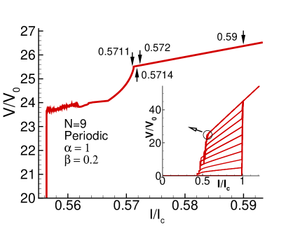
The CVC of the stack with 9 coupled JJ is presented in the inset to Fig. 1. It has a large hysteretic region with 9 branches. We show by circle the BPR on the outermost branch and its enlarged part in this figure. The arrows indicate the bias current values at which the detailed study of the charged dynamics have been done. We investigate the dependence of the electric charge in S-layer vs time at the following values of bias current and . We have done the FFT analysis of the charges oscillations at these values of current as well. As we mention in Ref.[8], the positions of the breakpoint in CVC and the onset of charge growth in S-layer in time dependence are not coincide.
3 Time stages in the nucleation of LPW
A correspondence between the breakpoint in CVC and charge dynamics in S-layers was demonstrated in the previous research.[8] Here we demonstrate that the creation and development of LPW has different stages in time (or current). We show that the breakpoint in CVC reflects just the region of sharp increase of the LPW amplitude. Investigation of the time dependence of electric charge in the S-layers give us the information concerning the nucleation of LPW.
At chosen values of and , the LPW with wave vector is created at the breakpoint.[4] Below we show the profiles of the charge oscillations and some enlarged parts for different values of bias current indicated in Fig. 1.
3.1 Fluctuation region
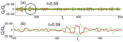
Fig. 2a shows the charge-time dependence for the first two S-layers of the stack with 9 coupled JJ at , which is far enough from the breakpoint in the outermost branch of CVC. We see that the charge value is practically the same in both layers and it is about , i.e. it is on the noise level. The charge oscillations here have mostly an irregular character. But nevertheless, as we can see in Fig. 2b, there are the regular oscillations in a short time interval with the frequency corresponding to the LPW. We call this part in CVC and the corresponding part in time dependence of the charge on the S-layers as a fluctuation region.
Let us clarify the shape of the charge signal we see in Fig. 2b . To do it, we demonstrate in Fig. 3 the time dependence of the voltages in the first and last junctions (left axis), which are the adjacent junctions to the first layer (we use the periodic BC and first layer has number 0). The charge density in the S-layer is expressed by the voltages and in the adjusting junctions , where , and is Debye screening length. On the right axes we plot the value of charge in the first S-layer, which is actually equal to at . At some time in during the oscillations the sign of charge in the first layer is changed: the vertical dashed lines show the sign changes of the difference .
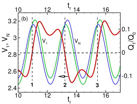
We see that at time moment corresponding to the first dashed line, the curve is getting above of curve , but at time moment corresponding to the second dashed line the situation is opposite and the charge in the first layer is getting negative. The time dependence of the voltage difference, i.e. charge in the first S-layer is shown by thick line. We see that the shape of the charge signal coincide qualitatively with the charge signal observed in Fig. 2b. Of course, the shape of charge signal might have some deviations from this one in the different layers. Its change in time reflects the character of Josephson junctions phase dynamics at different values of bias current. So, by shifting of voltages along the time axis in the Fig. 3, we may reproduce different shape of the charge signal ( particularly that one which appears in Fig. 2b).
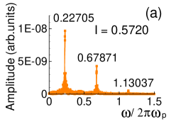
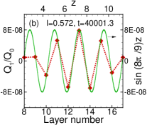
The spectrum of Fast Fourier Transformation (FFT) analysis of the charge oscillations in the first S-layer in the fluctuation region is shown in Fig. 4a. As it’s expected, it is broad and degraded. But nevertheless it demonstrates the manifestation of the LPW (maximum in the interval 0.22-0.25) and the Josephson oscillations (maximum in the interval 0.43-0.48). Of course, the charge distribution along the stack deviates from the wave with , as we can see in Fig. 4b. The solid line shows the , the rhombus show the charge value in the first S-layer at some fixed time moment .

3.2 Island region
With approaching the breakpoint on the outermost branch, the number of such intervals of regular oscillations we demonstrated in Fig. 2b is increasing and there size along time axes as well. The most important fact in this case is the value of the oscillations amplitude. It exceeds the noise value essentially now. So, we call such regions like the region shown in Fig. 5a at as the ”island regions”.
Fig. 5a shows the charge-time dependence for first two S-layers of the stack in the island region and Fig. 5b shows the enlarged part marked by circle in this region. We see that the amplitude of charge oscillations in shown island might have a value up to .
In the island region we can precisely determine the LPW frequency by the FFT analysis in contrast to the fluctuation region. In Fig. 6a we demonstrate the results of FFT analysis for charge oscillations at . As we can see, there is still the broadening part in the FFT spectrum, but the charge distribution along the stack follows the modulated LPW with (see Fig. 6b ).
3.3 Alternative amplitude region
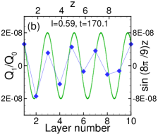
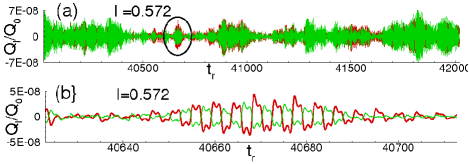
With increase in time (decrease in current) the islands are growing, joining, forming the region of charge oscillations with alternating amplitude. The characteristic part of it is shown in Fig. 7a. The amplitude of oscillation here is around , i.e. one order of value exceeds the noise level.
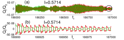
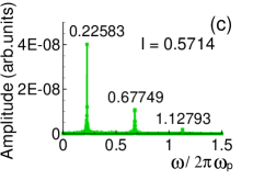
In Fig. 7b we show the enlarged part of charge oscillations in the time interval (186900, 187000). We can see clear here that the charge amplitude in the second layer is smaller than in the first one. It shows that the LPW is not the -mode, where and the amplitude is the same in all layers. As we mentioned above, the LPW with is created in the stack with 9 coupled JJ at and . In Fig. 7c we demonstrate the results of FFT analysis for charge oscillations in the first S-layer at . The LPW frequency is which is practically twice smaller than the Josephson frequency .
3.4 Growing region
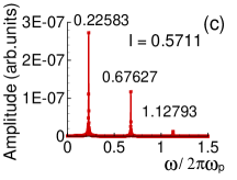
In Fig. 8a and Fig. 8b we demonstrate the charge oscillations and some enlarged part for the beginning of the region with growing amplitude. Fig. 8b demonstrates clear the fact that the amplitudes of the charge oscillations in the neighboring layers in the growing region is essentially different. Fig. 8c shows the results of FFT analysis of the charge oscillations in the first S-layer at bias current . The peaks are very narrow and sharp as it should be at the resonance condition. In this region the Josephson frequency is equal to the LPW frequency very precisely.
So, we may distinguish clearly four different stages in time development of LPW: the fluctuation region (LPW in short time interval on the noise level); the island region (with charge oscillations exceeding the noise level); the alternating amplitude region (all islands are joined), and the growing region (charge oscillations with growing amplitude).
4 Effects of noise level and external radiation on the LPW nucleation
Let us briefly discuss the possibility of affecting the process of LPW’s nucleation. First we present the results concerning the influence of the level of noise in bias current. As it was mentioned above, we add a small noise with amplitude in bias current in our calculations. The noise stimulates the appearance of difference of the phase differences in neighbor junctions. It leads to some distribution of the charge in the S-layers along the stack. At current values much larger than this distribution of charge attenuates in time. Approaching the breakpoint, the corresponding oscillations are increasing, especially in the growing region.
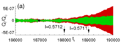
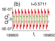
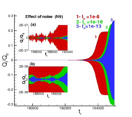
Fig. 9 demonstrates the time dependence of the charge in the first superconducting layer of the stack with nine coupled JJ in the beginning of the growing region for three values of the noise amplitude: and . It shows a remarkable fact that the noise with larger amplitude creates the LPW at smaller time (current) values, than the noise with the smaller amplitude. The inset (a) allows us to see clear that the growing region starts first in case of the noise amplitude equal to and the inset (b) demonstrates that for the noise amplitude the growing region starts in the last turn. This result is understandable: it’s easier to arrange a difference between neighbor junctions by larger value of the noise amplitude.
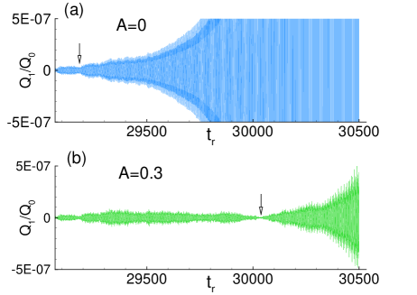
The another possibility to affect the nucleation process is the effect of the external radiation. If we irradiate a stack of Josephson junctions with microwave of frequency , it causes an alternating current through the stack. This alternating current can be described as the additional applied current , where A is a dimensionless amplitude.
In Fig. 10 we demonstrate the effect of radiation on the charge oscillations in the first S-layer in the beginning of the growing region. We see that the radiation with frequency and amplitude (Fig. 10b) shifts the starting point of growing region (shown by arrow) in comparison with case (Fig. 10a). Our results show that the change in the frequency leads to the shift of this point and additional resonance features. This effect of radiation will be considered in detail somewhere else.
We would like to mention here that the nucleation process can be affected by change in temperature as well. The change in the McCumber parameter should lead to the creation of the LPW with another wave number[4] and, correspondingly, to the nucleation process specific to this wave number .
In summary, we studied the nucleation of the longitudinal plasma wave in the coupled system of IJJ in HTSC and found the different stages in its process of development. The answer to the question concerning the correspondence between the breakpoint’s position in CVC and the parametric resonance region in time dependence of the charge on the S-layers is found. We showed that the position of the breakpoint on the outermost branch of CVC is related to the region with sharp increase of the amplitude of charge oscillation in the superconducting layers. We demonstrated that the onset of the growing region can be shifted by noise in the bias current and microwave radiation. These effects open a way to regulate the process of LPW nucleation in the stack of IJJ.
We thank M. R. Kolahchi, R. Kleiner, M. Suzuki and S. Flach for fruitful discussions. This research was supported by the Russian Foundation for Basic Research, grant 08-02-00520-a.
References
- [1] \NameKleiner R., Steinmeyer F., Kunkel G. Muller P. \REVIEWPhys. Rev. Lett.6819922394.
- [2] \NameKoyama T., Author S. Tachiki M. \REVIEWPhys. Rev. B54199616183.
- [3] \NameMachida M., Koyama T. Tachiki M. \REVIEWPhysica C300199855.
- [4] \NameShukrinov Yu. M. Mahfouzi F. \REVIEWPhys. Rev. Lett.982007157001.
- [5] \NameSakai S., Bodin P. Pedersen N.F. \REVIEWJ. Appl. Phys7319932411.
- [6] \NameMachida M., Koyama T., Tanaka A. Tachiki M. \REVIEWPhysica330200085.
- [7] \NameShukrinov Yu. M., Mahfouzi F. Seidel P. \REVIEWPhysica C449200662.
- [8] \NameShukrinov Yu. M., Mahfouzi F. Suzuki M. \REVIEWPhys. Rev. B782008134521.
- [9] \NameY. Matsuda et al \REVIEWPhys. Rev. Lett.7519954512.
- [10] \NameL. Ozyuzer et al \REVIEWScience31820071291.
- [11] \NameIrie A., Shukrinov Yu. M. Oya G. \REVIEWAppl. Phys. Lett.932008152510.
- [12] \NameRyndyk D. A. \REVIEWPhys. Rev. Lett.8019983376.