Proposal for manipulating and detecting spin and orbital states of trapped electrons on helium using cavity quantum electrodynamics
Abstract
We propose a hybrid architecture in which an on-chip high finesse superconducting cavity is coupled to the lateral motion and spin state of a single electron trapped on the surface of superfluid helium. We estimate the motional coherence times to exceed , while energy will be coherently exchanged with the cavity photons in less than ns for charge states and faster than s for spin states, making the system attractive for quantum information processing and strong coupling cavity quantum electrodynamics experiments. The cavity is used for non-destructive readout and as a quantum bus mediating interactions between distant electrons or an electron and a superconducting qubit.
The field of experimental quantum information processing has made significant progress in recent years. Many different physical implementations are being actively explored, including trapped ions leibfried_experimental_2003 ; haffner_scalable_2005 , semiconductor quantum dots petta_coherent_2005 ; koppens_driven_2006 , and superconducting qubits steffen_measurement_2006 ; dicarlo_demonstration_2009 . In particular, the strong coupling to microwave photons possible in circuit quantum electrodynamics (QED) architectures wallraff_strong_2004 has sparked interest in creating hybrid quantum systems capable of combining the advantages of different qubit implementations. In these proposals, a superconducting transmission line cavity acts as an interface between superconducting circuits and microscopic quantum systems, such as polar molecules andre_coherent_2006 ; rabl_hybrid_2006 , electron spins imamoglu_cavity_2009 ; wesenberg_quantum_2009 or ultra-cold atoms verdu_strong_2009 , typically with smaller couplings but much better coherence than superconducting qubits. Single electrons trapped above the surface of superfluid helium Andrei1997 might play a unique role as they can independently form a strongly coupled cavity QED system or act in concert with superconducting qubits.
Interest in electrons on helium is motivated in part by their exceptional properties, including the highest measured electron mobility shirahama_surface_1995 and long predicted spin coherence times lyon_spin-based_2006 . For these reasons the system was used in one of the first quantum information processing proposals platzman_quantum_1999 . The initial proposal focused on the motional states of a single trapped electron normal to the helium surface dykman_qubits_2003 , which promise long coherence times but have transition frequencies in the inconvenient range of GHz. Further, the electrons were to be detected destructively. More recently it has been proposed to use electron spins lyon_spin-based_2006 , and the possibility of moving electrons at MHz rates was demonstrated sabouret_signal_2008 , but it was not clear how to best read-out or couple such spin states.
Here, we address these challenges using the circuit QED architecture wallraff_strong_2004 , and show that both the electron’s motion and spin can be used to reach the strong coupling limit of cavity QED, where the coupling between the electron and cavity is larger than their decoherence rates, allowing for a wide variety of quantum optics and quantum information experiments. The quantized in-plane motion, parallel to the helium surface, can be engineered to have transition frequencies of a few GHz and is readily coupled to an on-chip cavity for non-destructive readout analogous to that used for superconducting qubits wallraff_strong_2004 or electron cyclotron motion in g-2 experiments Peil1999 . The cavity also mediates interactions between individually trapped electrons allowing for multi-qubit gates similar to those demonstrated in superconducting systems dicarlo_demonstration_2009 . In addition, the spin-photon coupling would be significantly enhanced by a controllable spin-orbit coupling.
The trapped electrons can be considered as quantum dots on helium operating in the single electron regime. These dots would be sufficiently small (sub-micron) that the lateral spatial confinement and potential depth will determine the orbital properties. A Jaynes-Cummings coupling between in-plane states and out-of-plane states in such dots was proposed recently zhang_jaynes-cummings_2009 . The feasibility of creating such nano-scale traps is buoyed by a recent experiment which has detected single electron tunneling events papageorgiou_counting_2005 . However, so far there have been no observations of either intradot quantization or spin resonance on helium.
It is instructive to compare electrons on helium with semiconductor quantum dots. In most traditional two dimensional electron gases (2DEG’s) such as in GaAs, the electrons form a degenerate gas with small effective masses, renormalized g-factors, and strong interactions with the lattice. In particular the strong piezoelectric coupling leads to short coherence times for the motional states ( ps) fujisawa_spontaneous_1998 . For this reason spin is typically used petta_coherent_2005 ; koppens_driven_2006 , but its coherence time can be strongly affected by nuclear spins johnson_triplet-singlet_2005 . In contrast, electrons on helium form a 2DEG at the interface between vacuum and superfluid, retaining their bare mass and g-factor. With the techniques described here, single electron quantum dots on helium promise some advantages over traditional semiconducting dots. We predict the decay of the orbital states to be times slower than in GaAs. Further, superfluid 4He has no nuclear spins ( natural abundance of 3He), leading to long predicted spin coherence timeslyon_spin-based_2006 , which are primarily limited by current noise in the trap leads. Perhaps most importantly, electrons on helium is a fascinating system where coherent single particle motion has not been accessible until now.
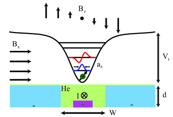
An electron near the surface of liquid helium experiences a potential due to the induced image charge of the form , with and . Together with the 1 eV barrier for penetration into the liquid, the image potential results in a hydrogen-like spectrum of motion normal to the surface, with effective Rydberg energy K and Bohr radius nm Andrei1997 . At the working temperature of mK the electron will be frozen into the ground out-of-plane state, and the helium will be a superfluid with negligible vapor pressure.
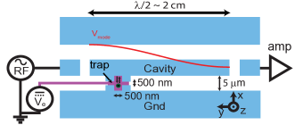
With the vertical motion eliminated, the electron’s lateral motion within an electrostatic trap could be coupled to the electric field of a superconducting transmission line cavity. As shown in Fig. 2, the cavity center-pin and ground plane form a split-guard ring around a positively biased trap electrode. We approximate the trapping potential in each of the lateral dimensions as being nearly parabolic, with level spacing . We assume a single electron in a high-aspect ratio trap so that the and motional frequencies are distinct, with . The Hamiltonian of the electron near the potential minimum can be approximated as
| (1) |
Here, is the standard deviation of the motional ground state wavefunction and is the anharmonicity. Because the trap is small and the potential must flatten at the outer electrodes, . The to transition frequency is . The electron motion can be treated as a qubit when is larger than the decoherence rates. The scaling of the system parameters with geometry (see Fig. 2) can be estimated analytically by approximating the trap potential as . In this case , , and . Therefore one can tune the motional frequency by adjusting the bias voltage, determine the anharmonicity by the trap size (confinement effects), and trade-off sensitivity in bias voltage for sensitivity to trap height (generally so as to avoid exponential sensitivity to film thickness).
The microwave environment and the trapping potential are simulated using Sonnet®and Maxwell®, respectively and then Schrödinger’s equation is numerically solved to find the resulting wavefunctions for the geometry shown in Figs. 1 & 2. Using physically reasonable trapping parameters: helium depth , trap size , trapping voltage results in a trap depth deep enough to prevent thermal escape, and a transition frequency convenient to microwave electronics. The cavity can be represented by the Hamiltonian , with close to the desired motional frequency. The electron’s motion within the trap is affected by and induces an electric field in the microwave cavity. If the level spacing is in resonance with the energy of a cavity photon , the two systems can exchange energy at the vacuum Rabi frequency, where is the zero-point electric field in the cavity. This yields a Jaynes-Cummings Hamiltonian of the joint system , where is the motional quanta annihilation operator. The electron motional states can be manipulated quickly due to the large coupling strength , a consequence of the large electron dipole moment , and without exciting transitions to higher lateral states due to the anharmonicity .
In addition to the motional degree of freedom, the electron carries a spin degree of freedom. The bare coupling of cavity photons to the spin is many orders of magnitude weaker than to the charge, but can be enhanced via controlled spin-motion coupling. A different mechanism of enhancement for semiconducting double-dots was pointed out in childress_mesoscopic_2004 . A spin-quantization axis is established using a magnetic field in the direction (Fig. 2). The Larmor frequency per unit field is approximately . Niobium cavities have been demonstrated to maintain in parallel fields of up to , allowing Larmor frequencies of up to . Both the cavity and motion have so that they relax to the ground state.
We propose to create a non-uniform -field component with a gradient along the vibrational axis, , by passing a current through the center electrode (in the -direction see Fig. 2). This leads to a new term in the Hamiltonian, . The resulting spin-orbit interaction provides an enhanced cavity coupling , mediated through the motional state, where
| (2) |
This allows manipulation and readout of individual spins, as well as the use of coupling techniques developed for superconducting qubits dicarlo_demonstration_2009 . Further, the coupling is proportional to the applied current, allowing the spin-cavity to be tuned in-situ on nanosecond timescales. For a 1 mA current 500 nm away a field gradient can be created. If these parameters give kHz whereas if MHz then the coupling can be made large, MHz.
The current also creates a second-order variation in the -component of , leading to a new term in the Hamiltonian, . If the constant magnetic field is applied along the -direction, this term will lead to sideband transitions simultaneously changing the orbital and spin states for drives at . These transitions can be used to manipulate, cool, and detect the spin using its coupling to the lateral motion. With such cooling it might allow one to use smaller spin frequencies.
It is also important to consider decoherence of the motional and spin states. The two major sources of noise are electrical fluctuations in the leads and excitations in the liquid helium. Here we present a short summary of these decoherence mechanisms (also see Fig. 3). A detailed explanation of these mechanisms is presented in the supplementary materials eonhe_supplement .
A motionally excited electron can relax radiatively via spontaneous emission directly into free space, through the cavity, or the trap bias electrode. The electron radiates very little into free space, both because it is small (), and because the microwave environment is carefully controlled. In a perfectly symmetric trap, radiation through the bias leads would be suppressed by a parity-selection rule. We conservatively assume that the electron is displaced from the trap center by , which gives a relaxation rate . Though this mechanism is not expected to be dominant, it could be easily reduced significantly by engineering the impedance of the trap bias lead. In addition, slow fluctuations in the trap electrode voltage () can deform the potential, changing the motional frequency and resulting in dephasing. This can occur from drift in the voltage source, thermal Johnson voltage noise, or local “1/f” charge noise. Drift slow compared with the experiment time is easily compensated. The thermal noise at 50 mK is quite small with dephasing rate Hz. Any charge fluctuations in the bias leads should be screened by their large capacitance to ground but even conservatively assuming an anomolously small capacitance, we estimate a dephasing rate , which would not be the dominant decoherence rate. Noise from the cavity and ground plane electrodes should have less effect due to the symmetry of the potential.
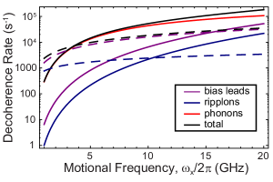
In addition to decoherence through the electrodes, the electron can lose coherence to excitations in the helium. Two major types of excitations are relevant: capillary waves on the helium surface, known as ripplons, and phonons in the bulk. The electron is levitated above the surface at height nm, which greatly exceeds the height of the surface fluctuations, and therefore coupling to ripplons is small. The characteristic electron speed significantly exceeds the speed of sound in He and the characteristic group velocity of ripplons. As a result, the rate of direct emission is suppressed and decay into ripplons is dominated by second order processes in which two ripplons of nearly opposite momentum simultaneously interact with the electron. The allowed phase volume is limited by the condition on the total ripplon momentum. Thus the corresponding decay rate is small, estimated to be s-1 (see Fig. 3).
The most important mechanism related to helium excitations is decay into phonons. The coupling to phonons is reminiscent of piezoelectric coupling in semiconductors. An electron creates an electric field that causes helium polarization, which in turn affects the electron. Phonons modulate the helium density and thus the polarization, which changes the electron energy. However, in contrast to semiconductors, where the typical piezoelectric constant is /cm2 Seeger2004 , its analog in He is cm2. Therefore coupling to phonons is much weaker than in semiconductors. The corresponding decay rate is (see Fig. 3).
Besides decay, coupling to helium excitations leads to fluctuations of the electron frequency and ultimately to dephasing. The major contribution comes from two-ripplon processes, since ripplons are very soft excitations with comparatively large density of states at low energies, so that they are excited even for low temperatures. However, because of the weak coupling, the dephasing rate remains small, for mK (see Fig. 3). It also decreases rapidly as the temperature is lowered. Another mechanism of dephasing are slow drifts in the helium film thickness, which change the trap frequency through its dependence on the height, , of the electron. Fortunately, the cavity forms a liquid He channel glasson_observation_2001 in which the film height is stabilized by surface tension, rendering it much less susceptible to low frequency excitations.
The electron spin promises much longer coherence times, and when uncoupled to the charge the lifetime is expected to exceed seconds lyon_spin-based_2006 . When the spin is coupled to the motion, it will also inherit the orbital decoherence mechanisms with a matrix element . These mechanisms can be further diminished by turning off the gradient field or changing the spin-motion detuning, to reduce the coupling. In addition to decoherence felt through the spin-orbit coupling, the electron spin can be dephased by fluctuating magnetic fields. These can arise from Johnson current noise in the leads which would lead to dephasing rates less than . It is also possible that the spin will be affected by “1/f” flux noise koch_flicker_1983 , often seen in SQUID experiments. The trap involves no loops or Josephson junctions, so it is difficult to predict to the extent of flux noise in this geometry, however even a worst case estimate still yields a dephasing rate of only eonhe_supplement .
In summary we use circuit QED to propose solutions to many of the problems associated with electrons on helium, developing the ability to manipulate and detect both the electron’s quantized motion and its spin. Further, this architecture couples electrons on helium to each other and to other quantum systems via single microwave photons, creating a scalable architecture for quantum computing.
The authors would like to acknowledge useful discussions with Forrest Bradbury. This work was supported in part by the NSF grants DMR-053377, EMT/QIS 0829854 and CCF-0726490. Institutional support was also provided by Yale University via the Quantum Information and Mesoscopic Physics Fellowship (DIS) and the Austrian Academy of Sciences through the DOC fellowship (AF).
References
- (1) D. Leibfried, et. al., Nature 422, 412 (2003)
- (2) H. Haffner, et. al., Nature 438, 643 (Dec. 2005)
- (3) J. R. Petta, et. al.,Science 309, 2180 (2005)
- (4) F. H. L. Koppens, et. al.,Nature 442, 766 (2006)
- (5) M. Steffen, et. al.,Science 313, 1423 (2006)
- (6) L. DiCarlo, et. al.,Nature 460, 240 (2009)
- (7) A. Wallraff, et. al.,Nature 431, 162 (2004)
- (8) A. Andre, et. al.,Nature Physics 2, 636 (2006)
- (9) P. Rabl, et. al.,Phys. Rev. Lett. 97 (2006)
- (10) A. Imamoglu, Phys. Rev. Lett. 102, 083602 (2009)
- (11) J. H. Wesenberg, A. Ardavan, et. al.,Phys. Rev. Lett. 103, 070502 (2009)
- (12) J. Verdu, H. Zoubi, et. al.,Phys. Rev. Lett. 103, 043603 (2009)
- (13) Two-dimensional electron systems on helium and other cryogenic substrates, edited by E. Y. Andrei (Kluwer, Boston, 1997)
- (14) K. Shirahama, S. Ito, H. Suto, and K. Kono, J. Low Temp. Phys. 101, 439 (1995)
- (15) S. A. Lyon, Phys. Rev. A 74, 052338 (2006)
- (16) P. M. Platzman and M. I. Dykman, Science 284, 1967 (1999)
- (17) M. I. Dykman, P. M. Platzman, and P. Seddighrad, Phys. Rev. B 67, 155402 (2003)
- (18) G. Sabouret, et. al.,Appl. Phys. Lett. 92, 082104 (2008)
- (19) S. Peil and G. Gabrielse, Phys. Rev. Lett. 83, 1287 (1999)
- (20) M. Zhang, H. Y. Jia, and L. F. Wei, Phys. Rev. A 80, 055801 (2009)
- (21) G. Papageorgiou, et. al.,Appl. Phys. Lett. 86, 153106 (2005)
- (22) T. Fujisawa, et. al.,Science 282, 932 (1998)
- (23) A. C. Johnson, et. al.,Nature 435, 925 (2005)
- (24) L. Childress, A. S. Sorensen, and M. D. Lukin, Phys. Rev. A 69, 042302 (2004)
- (25) Supplementary materials
- (26) K. Seeger, Semiconductor Physics: An Introduction, 9th ed. (Springer-Verlag, Berlin, 2004)
- (27) P. Glasson, et. al.,Phys. Rev. Lett. 87, 176802 (2001)
- (28) R. H. Koch and et. al., J. Low Temp. Phys. 51, 207 (1983)