Andreev reflection measurements in nanostructures with amorphous WCx superconducting contacts
Abstract
Point-contact Andreev reflection measurements of Co/ and Cu/tungsten-carbide (WCx) contacts are presented. Metallic thin films were patterned by e-beam-lithography and lift-off; tungsten carbide superconducting tips were grown directly on the pre-patterned samples by decomposition of a metallo-organic vapour (tungsten hexacarbonyl) under a focused Ga+-ion beam (FIB). Current-voltage measurements as a function of temperature and magnetic field clearly showed the signatures of Andreev reflection. The experimental conductance-voltage curves were analyzed within the Blonder-Tinkham-Klapwijk theory. The results highlight the possibilities, advantages and disadvantages of using FIB-produced amorphous WCx tips for point-contact spectroscopy in metallic nanostructures.
pacs:
74.45.+c,85.75.-d,73.40.-c1 Introduction
In recent years research activity has focussed on nanotechnological applications of superconducting and magnetic materials for quantum information technology and spintronics [1, 2]. There are various aspects of interest that cover both fundamental issues such as the value of the superconducting gap in tiny superconducting structures, the behaviour of the electronic density of states at interfaces as well as applications such as the measurement of the ferromagnetic spin polarization by Andreev reflection. The measurement and analysis of Andreev reflection [3, 4] in superconductor/ferromagnet (S/F) point contacts has proven to be potentially applicable for the determination of the spin polarization [5, 6, 7, 8], but was also found to be prone to misinterpretations [9, 10]. On the other hand, point contact spectroscopy could help to study systematically the physics of interfaces between two different materials, an issue of growing importance nowadays.
In this work the superconducting behaviour, i.e. current-voltage () characteristics and the corresponding differential conductance , of nm diameter WCx electrodes fabricated by a metallo-organic vapour deposition process was explored. It is shown that Andreev reflection is clearly observed at WCx contacts with normal as well as with ferromagnetic metals. The differential conductance curves, however, show variations in the local superconducting gap value upon the material on which the superconductor is deposited. Some of these curves have also an unconventional form that suggests either the formation of weak links in the WCx tip or the contribution of a narrow-band normal metal at the junction. In spite of its flexibility, it appears that the necessity of Ga+ion irradiation to produce the superconducting nanocontact with a focused ion beam (FIB) device influences the intrinsic properties of the bulk materials at their surfaces. Nevertheless, this influence should not be taken always as a disadvantage due to the new physics one may expect from these materials and at their interfaces. This work opens up the possibility of growing Andreev reflection test leads on a nanometer scale during the preparation and handling of different materials in a dual beam microscope.
2 Experimental Details
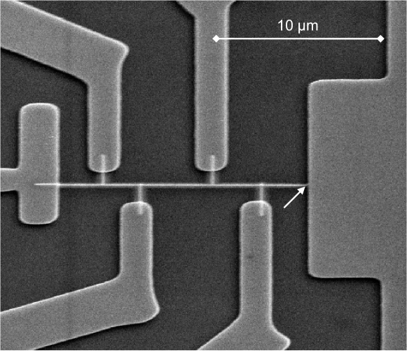
For e-beam lithography, sample imaging and metallo-organic vapour deposition a dual beam microscope (DBM), model FEI NovaLabXT 200, equipped with the Raith ELPHY Plus electron lithography system was used. The sample preparation was realized in two stages. In the first step the contact layout structure allowing for Andreev reflection measurements in four-point configuration was fabricated. To this end Si substrates coated with 150 nm thick SiN films were spin-coated with a positive resist and the sample layout was transferred to the resist by e-beam lithography. After developing and cleaning Co or Cu thin films were sputtered onto the substrates at a base pressure of mbar using metallic targets of % purity. The following lift-off concluded the first sample preparation stage with the production of the contact structure, see Fig. 1.
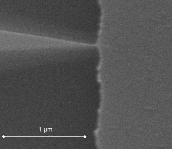
In the second stage the facilities offered by the DBM were employed, especially the deposition of metallic films in nanometer dimensions from the induced decomposition of a chemical precursor over a substrate by the ion beam. This technique is known as ion-beam-induced- or -assisted-deposition (IBID or IBAD). The main advantage of this technique is the deposition of the material in principally any shape and size without a mask directly onto the substrate. For the growth of the superconducting WCx tips tungsten hexacarbonyl, W(CO)6, was used as a precursor. WCx deposition was done under Ga+ ion irradiation with a beam energy of 30 keV and a focused ion-beam current of 98 pA. The precursor temperature was set to 56∘C; during the film deposition the pressure in the chamber was mbar. In this way superconducting nanowires with a cross-section of nm nm were deposited. The end of the nanowire making the contact to the metal under investigation (see arrow in Fig. 1) was made in a needle shape such that the contact area is estimated to be circular with a diameter of about nm. This tip is shown in Fig. 2 for the WCx/Co sample.
The fabrication of the metallic films and nanocontacts was done in high vacuum which is advantageous over the conventional mechanical point-contact technique [11]. Furthermore, several WCx tips can be grown on the same substrate such that it would be possible to study the spatial variation of the properties at the interfaces like the spin-polarization. The tungsten to carbon ratio in WCx varies slightly from sample to sample, but nevertheless the critical temperatures were consistently around 5 K in agreement with previous reports [12, 13]. In spite of these advantages we note that the IBID process may produce a non-negligible change in the intrinsic properties of the material surface to be investigated. The changes depend on the acceleration energy of the Ga+-ions used, the mass density and other intrinsic properties of the material in question. We note that the properties of these interfaces were not yet studied systematically in the past. An anomalous behavior of the differential conductance, for example, may imply the existence of unconventional material properties at the interfaces.
After preparation, the samples were mounted in a standard chip carrier. Contacts were made by Au wires and silver paste. Current-voltage (–) measurements in four-point configuration were made with a Keithley DC and AC current source (Keithley 6221) and a nanovoltmeter (Keithley 2182). The measurements were performed in a He-flow cryostat (Oxford Instruments) in the temperature range between 2 K and 300 K with a temperature stabilization better than 1 mK.
3 Results and Discussion

Recently published work [12] reported that WCx nanowires produced via the IBAD technique are superconducting; we have reported [13] similar results on our WCx nanowires, where critical temperatures K were found. These critical temperatures are in good agreement with values from amorphous thin films of W and C produced by RF sputtering [14]. The upper critical field was T defined at 90% of the normal state resistance [13]. In situ energy dispersive X-ray analysis (EDX) was used to study the composition of the WCx wires and yielded concentrations of about 35% C, 4% O, 13% Ga, 3% Se, 28% Si and 17% W. The tungsten concentration is in agreement with the data from Refs. [13, 14, 15, 16].
Figure 3 shows the temperature dependence of a Co/WCx point-contact resistance. A clear transition in the resistance is seen when the sample enters into the superconducting state and at 5 K a constant, residual resistance is reached. This residual resistance is not zero, but finite with a value of for this contact which is just the resistance of the Co metal in the current path. For the Cu/WCx junctions we obtained K and . The temperature dependence of the resistance of the Co/WCx sample showed a linear behaviour above 45 K with a negative temperature slope, see Fig. 3, a resistivity ratio and a normal state resistivity of about 140 cm at room temperature. A similar dependence was obtained for the Cu/WCx samples. More details about the electrical properties, especially the temperature and magnetic field dependence of these WCx wires were reported in [13]. Point-contact spectroscopy measurements were performed on several samples of the same deposited metallic system. Here the results for representative Cu and Co electrodes are presented.
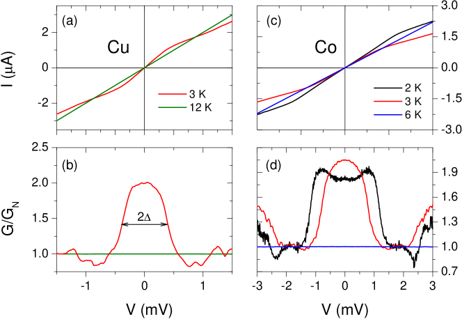
Figure 4 presents the – characteristics of a WCx/Cu and a WCx/Co point contact measured at various temperatures. At higher temperatures above the critical temperature of the WCx nanowire the – curves were linear. Below the critical temperature a clear nonlinearity was observed. This behaviour is even more obvious in the conductance-voltage characteristics where the conductance was obtained from the measured – curves by numerical differentiation. These curves show that the WCx nanocontacts support Andreev reflection.
¿From BCS theory the zero temperature gap of the WCx wires is estimated to meV (Co/WCx) or meV (Cu/WCx). At 3 K the superconducting gap was determined from the conductance vs. voltage curves as meV for the Cu/WCx (in comparison with the BCS value KmeV) and meV for the Co/WCx contact (KmeV), respectively. Whereas for the latter the value of the superconducting gap is 17% larger than the expected one from BCS, the value of the gap for the Cu-based contact is 22% smaller. These differences are probably due to interfacial defects.
In the ideal case, at low temperatures and in the subgap voltage regime the conductance of a superconductor/normal metal contact should be twice as large as the normal state conductance. This is seen in both junctions, see Fig. 4. However, we observe clear deviations from the conventional form of the conductance curve with minima at higher voltages, i.e. at , see Figs. 4 and 6. Similar deviations were reported before [17, 18, 19, 20, 5, 21, 22, 23, 24, 25, 26, 27] and are characterized by conductance values less than the normal state value at . This behaviour could be understood either by the formation of a weak link [18, 19, 20] or by the contribution of a narrow band normal material [28], both might be formed at the junction interface. Also, it might well be that the weak-link itself behaves as a narrow band normal material. It can be shown [28] that for a junction between a superconductor with gap and a normal metal with a band width of the order of the energy gap, a negative differential conductance appears at voltages . For example, for transmittivity and a clear (negative) minimum appears in at [28]. In all samples the location of the conductivity minimum appears to scale with the value of the gap. This may appear unlikely if we assume the existence of this kind of normal metal independently of the attached superconductor. However, this narrow band material or the material of the weak link at the interface may be formed by the contact to the superconducting material and therefore a direct correlation with the superconducting energy gap can exist. Phenomenologically speaking, the observed behavior can be quantitatively understood assuming a parallel contribution by a material that allows the current to pass through the junction within an energy band of the order but larger than the energy gap of the superconducting part.
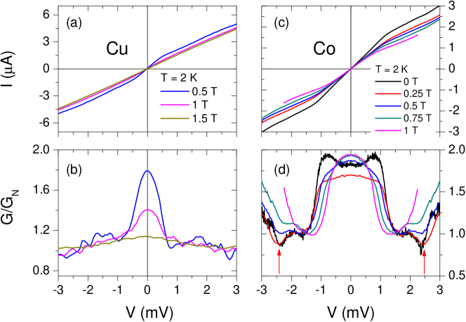
The magnetic field dependence at constant temperature was also investigated with the results for the two junctions shown in Fig. 5. The magnetic field reduces the zero bias conductance enhancement and smears out the bias dependent features. Note that the conductance minimum in Fig. 5(d), marked by the red arrows, is systematically removed by the magnetic field. This indicates that these features are actually linked to the superconducting state. Similar magnetic field effects were observed in experiments on MgB2 [29] and were explained as a consequence of the pair-breaking effect; note, however, that MgB2 is a standard example of a superconductor with two intrinsic energy gap values. The field dependence observed here corroborates the interpretation of the conductance-voltage curves as arising from Andreev reflection.
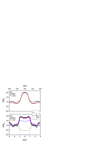
The experimental data were analyzed within the Blonder-Tinkham-Klapwijk (BTK) model [30] and the narrow band model [28]. In the BTK model the quality of the interface is characterized by a dimensionless parameter for the barrier strength, conventionally denoted , with corresponding to a clean interface and corresponding to the presence of a tunnelling barrier between superconductor and metal. The transmittivity used in [28] can be expressed as , where was defined in [30]. Notice that and means and 0.
From the result for both junctions one might tentatively conclude that , i.e. that the barrier is comparatively clean. Figure 6 shows conductance data in comparison to calculations within the BTK model. Reasonable agreement was found for subgap voltages. The parameters used in the BTK calculations were , a spin polarization and a gap to temperature ratio K for the Cu/WCx junction as well as and K) for the Co/WCx junction. The gap to temperature ratios needed to fit the data using the BKT formulas are significantly larger than the ones determined independently from the measured temperature and gap values as we showed above. In other words the curves at the measured temperatures for both cases are significantly sharper than expected from the BKT calculations, a fact that may indicate a non-BCS temperature behaviour very probably related to the interfacial properties. Also the vanishing spin polarization of the Co/WCx contact can be due to radiation defects at the Co surface introduced in the fabrication process. It might as well be related to the inferior crystallographic quality of our sputter-deposited Co films.
The conductance minima at larger voltages as well as the increase in at voltages above the minimum at , see Fig. 6(b), cannot be reproduced within the BTK model of a normal/superconducting contact. Assuming that at the interface of the junction a weak link of a material that behaves as having a band width contributing in parallel to the measured current, one can reasonably well reproduce the observed minimum due to the negative differential conductivity contribution, see Fig. 6(a). In a similar way one can understand the observed minimum in the Co/WCx junction, decreasing in this case the absolute band width of the weak link material, see Fig. 6(b). The observed conductance increase at voltages might be due to nonlinear contributions to the tunnelling conductance as discussed in the Simmons’s model [31].
4 Conclusions
In this work it was shown that Andreev reflection can be observed in point contacts between Cu and Co films and WCx tips deposited by metallo-organic vapour deposition in a dual beam microscope. Qualitatively the measured temperature and magnetic field dependence of the differential conductivity agree with the expectations. The Co films investigated here did not appear to be spin-polarized at the contact region according to the conventional BTK model for a ferromagnet/superconductor contact. On the other hand the parameters needed to fit the experimental curves at relatively high temperature appear to be inconsistent with the BCS expectations. The anomalies observed in the differential conductivity at voltages above the energy gap values suggest a weak link formation with narrow band properties contributing in parallel at the interfaces of the contacts. In spite of the disadvantages Ga irradiation may have when used to deposit the WCx amorphous superconductor, the presented method holds future potential in the preparation of Andreev contacts for spin-polarization measurements on the several nanometer scale, offering fast and reliable sample preparation and the possibility to determine the spatial variation of the spin-polarization. Systematic measurements using different materials can be used in the future to study in more detail the properties of interfaces, which can be modified using FIB within a dual beam microscope.
References
References
- [1] Prinz G A 1995 Physics Today 48 58–63
- [2] Daughton J M, Pohm A V, Fayfield R T and Smith C H 1999 Journal Physics D: Applied Physics 32 R169–R177
- [3] Mazin I I 1999 Phys. Rev. Lett. 83 1427–1430
- [4] Andreev A F 1964 Soviet Physics JETP 19 1228–1231
- [5] Soulen, Jr R J, Byers J M, Osofsky M S, Nadgorny B, Ambrose T, Cheng S F, Broussard P, Tanaka C T, Nowak J, Moodera J S, Barry A and Coey J 1998 Science 282 85–88
- [6] Upadhyay S K, Palanisami A, Louie R N and Buhrman R A 1998 Physical Review Letters 81 3247–3250
- [7] Ji Y, Strijkers G J, Yang F Y, Chien C L, Byers J M, Anguelouch A, Xiao G and Gupta A 2001 Physical Review Letters 86 5585–5588
- [8] Nadgorny B, Soulen, Jr R J, Osofsky M S, Mazin I I, Laprade G, van de Veerdonk R J M, Smits A, Cheng S F, Skelton E F and Qadri S 2000 Physical Review B 61 R3788–R3791
- [9] Auth N, Jakob G, Block T and Felser C 2003 Physical Review B 68 024403–1–6
- [10] Bugoslavsky Y, Miyoshi Y, Clowes S K, Branford W R, Lake M, Brown I, Caplin A D and Cohen L F 2005 Phys. Rev. B 71 104523
- [11] Blonder C E and Tinkham M 1983 Physical Review B 27 112–118
- [12] Sadki E S, Ooi S and Hirata K 2005 Physica C 426-431 1547–1551
- [13] Spoddig D, Schindler K, Rödiger P, Barzola-Quiquia J, Fritsch K, Mulders H and Esquinazi P 2007 Nanotechnology 18 495202–1–6
- [14] Bond W L, Cooper A S, Andres K, Hull G W, Geballe T H and Matthias B T 1965 Physical Review Letters 15 260–261
- [15] Koh Y B, Gamo K and Namba S 1991 Journal of Vacuum Science and Technology B 9 2648–2652
- [16] Jenkins D W K, Allen G C, Prewett P D and Heard P 1991 Journal of Physics: Condensed Matter 3 S199–S206
- [17] Rowell J M and Feldmann W L 1968 Phys. Rev. 172 393
- [18] Klapwijk T M, Blonder G E and Tinkham M 1982 Physica 109&110B 1657
- [19] Octavio M, Tinkham M, Blonder G E and Klapwijk T M 1983 Phys. Rev. B 27 6739
- [20] Flensberg K, Hansen J B and Octavio M 1988 Phys. Rev. B 38 8707
- [21] Wei J Y T, Yeh N C, Garrigus D F and Strasik M 1998 Phys. Rev. Lett. 81(12) 2542–2545
- [22] Soulen R J, Osofsky M S, Nadgorny B, Ambrose T, Broussard P, Byers J, Tanaka C T, Nowak J, Moodera J S, Laprade G, Barry A and Coey J M D 1999 J. Appl. Phys. 85 4589
- [23] Rourke P M C, Tanatar M A, Turel C S, Berdeklis J, Petrovic C and Wei J Y T 2005 Phys. Rev. Lett. 94(10) 107005 see also the comments from G. Sheet and P. Raychaudhuri, Phys. Rev. Lett. 96, 259701 (2006), and W. K. Park and L. H. Greene Phys. Rev. Lett. 96, 259702 (2006), and the reply from the authors in Phys. Rev. Lett. 96, 259703 (2006).
- [24] Panguluri R P, Zeng C, Weitering H H, Sullivan J M, Erwin S C and Nadgorny B 2005 phys. stat. sol. (b) 242 R67
- [25] Strijkers G J, Ji Y, Yang F Y, Chien C L and Byers J M 2001 Phys. Rev. B 63 104510
- [26] Panguluri R P, Ku K C, Wojtowicz T, Liu X, Furdyna J K, Lyanda-Geller Y B, Samarth N and Nadgorny B 2005 Phys. Rev. B 72(5) 054510
- [27] Yun S H, Anderson N, Liang B, Greene R L and Biswas A arXiv:0712.1614
- [28] García N and Esquinazi P arXiv:0903.2237
- [29] Szabó P, Samuely P, Kačmarčík J, Klein T, Marcus J, Fruchart D, Miraglia S, Marcenat C and Jansen A G M 2001 Physical Review Letters 87 137005–1–4
- [30] Blonder G E, Tinkham M and Klapwijk T M 1982 Physical Review B 25 4515–4532
- [31] Simmons J G 1963 J. Appl. Phys. 34 1793