Orbital photogalvanic effects in quantum-confined structures
Abstract
We report on the circular and linear photogalvanic effects caused by free-carrier absorption of terahertz radiation in electron channels on (001)-oriented and miscut silicon surfaces. The photocurrent behavior upon variation of the radiation polarization state, wavelength, gate voltage and temperature is studied. We present the microscopical and phenomenological theory of the photogalvanic effects, which describes well the experimental results. In particular, it is demonstrated that the circular (photon-helicity sensitive) photocurrent in silicon-based structures is of pure orbital nature originating from the quantum interference of different pathways contributing to the absorption of monochromatic radiation.
pacs:
78.40.Fy, 72.40.+w, 73.40.Qv, 78.20.-eI Introduction
The photogalvanic effects, linear (LPGE) and circular (CPGE), representing the generation of a directed electric current due to the asymmetry of photoexcitation or relaxation processes attract growing attention. They can occur in media of sufficiently low spatial symmetry only and are known to be an efficient tool to study nonequilibrium processes in semiconductor structures yielding information about their symmetry, details of the band spin splitting, momentum, energy and spin relaxation times etc. (see e.g. [SturmanFridkin_book, ; Ivchenko_book, ; GanichevPrettl, ; IvchenkoGanichev_book, ]). Moreover, the photogalvanic effects are applied for the detection of the polarization state of infrared and terahertz (THz) laser radiation. JAP2009 The low spatial symmetry required for the photogalvanic effects is naturally realized in non-centrosymmetric semiconductors and low-dimensional structures based on them. However, it has been shown that both the LPGE and the CPGE can occur in two-dimensional structures made of centrosymmetric crystals, e.g. silicon, due to the structure inversion asymmetry. Magarill89 ; IvchenkoPikus_book ; Tarasenko07 While the LPGE in silicon metal-oxide-semiconductor field-effect-transistors (Si-MOSFETs) was observed almost twenty years ago, Gusev87 first experiments on the CPGE have been reported only most recently. Olbrich09 Besides the fundamental interest to photogalvanics, a renaissance in the study of photoelectrical phenomena in MOSFETs is additionally stimulated by promising applications for the emission and detection of terahertz radiation. Knap09 Here, we present a comprehensive experimental and theoretical study of the THz radiation induced photogalvanic effects in Si-MOSFETs fabricated on (001) precisely oriented as well as on miscut surfaces. The fact of the existence of the circular (photon-helicity sensitive) photocurrent, which reverses its direction upon changing the sign of the circular polarization, in Si-based structures is of particular interest. It demonstrates that the CPGE current caused by the transfer of photon angular momenta to free carriers can be generated not only in structures with a strong spin-orbit interaction due to spin-dependent optical excitation, Ganichev01 ; GanichevPrettlreview ; Bieler05 but even in systems with a vanishingly small constant of spin-orbit coupling. We show that the CPGE in Si-MOSFETs excited by THz radiation originates from the quantum interference of different pathways contributing to the radiation absorption. Tarasenko07 ; Olbrich09
This paper is organized as follows. In Sec. II, we present the phenomenological theory of the LPGE and CPGE in two-dimensional channels on (001) precisely oriented structures as well as on miscut silicon surfaces. In Sec. III, a short overview of the used experimental technique is given. The experimental results are summarized in Sec. IV and compared with the phenomenological theory. In Sec. V, we present a microscopic theory of the CPGE caused by the quantum interference of optical transitions for both types of structures. Finally, in Sect. VI, we discuss the experimental data in view of the theoretical background.
II Phenomenological theory
Phenomenologically, the density of the photocurrent emerging in an unbiased structure within the linear regime in the radiation intensity is given by IvchenkoPikus_book
| (1) |
where is a third-rank tensor being symmetric in the last two indices, is a second-rank pseudotensor, is the electric field of the radiation in the channel, is the (complex) unit vector of the light polarization, , and are the Cartesian coordinates, and the photon wave vector is neglected in Eq. (1). The tensor describes the photocurrent, which can be induced by linearly polarized or unpolarized radiation. By contrast, stands for the photocurrent, which is sensitive to the radiation helicity and reverses its direction upon switching the sign of the circular polarization, because with the degree of circular polarization and the unit vector pointing in the light propagation direction. Non-zero components of the tensors and can be obtained by analyzing the spatial symmetry of structures.
We consider the linear and circular photogalvanic effects for the two point-group symmetries and , which are relevant to electron channels on precisely (001) oriented and miscut silicon surfaces, respectively. Two-dimensional channels on a (001) surface can be effectively described by the axial point-group , which takes into account the structure inversion asymmetry of the channel. In such structures, the photocurrent can be excited only at oblique incidence of radiation, and its components are given by the phenomenological equations
| (2) | |||
where the first and second terms on the right-hand side of Eqs. (2) stand for the linear and circular photogalvanic effects, respectively, and are the in-plane axes, and is the channel normal.
The channels fabricated on miscut surfaces exhibit the lower point-group symmetry due to the deviation of the channel plane from together with the asymmetry of the confinement potential. Magarill89 ; IvchenkoPikus_book In structures of the point group, both linear and circular photogalvanic effects are allowed even at normal incidence of radiation. GanichevPrettlreview In this particular geometry, the photocurrent components are phenomenologically described by
| (3) | |||||
Here, we assume that the channel plane is tilted from the plane around the axis , and is the channel normal. In contrast to -oriented MOSFETs, the photocurrent in structures on miscut surfaces can be induced even by unpolarized radiation.
III Samples and experimental techniques
In our experiments, we study photocurrents in MOSFETs fabricated on (001)-oriented and miscut silicon surfaces. On the precisely (001)-oriented surface, a transistor along with a channel length of mm and a width of mm was prepared with a nm thick SiO2 layer, a semitransparent polycrystalline Si gate and a doping level of the depletion layer of about cm-3. In this transistor, the variation of the gate voltage Vg from to V changes the carrier density from about to cm-2 and the energy spacing between the size-quantized subbands and from to meV. The peak mobilities at room and helium temperature are and cm2/Vs, respectively. Another set of MOSFETs was fabricated on miscut surfaces tilted by an angle of or from the -plane around . Two transistors were prepared on each miscut substrate, one oriented along and the other along the inclination direction . They have a size of mm2, semitransparent Ti gates of nm thickness and a doping concentration of about cm-3. A variation in the gate voltage from 1 to V changes the carrier density from to cm-2 and the energy spacing from to meV. The peak electron mobilities in the channel are about 103 and cm2/Vs at and K, respectively. The MOSFETs on miscut surfaces have a nm thick SiO2 layer.
For optical excitation we use the emission of a terahertz molecular gas laser, optically pumped by a transversely excited atmosphere pressure (TEA) CO2 laser.GanichevPrettl With NH3 as active gas, 100 ns pulses of radiation with a peak power 30 kW are obtained at the wavelengths 76, 90, 148 and 280 m (corresponding to the photon energies 16.3, 13.7, 8.4 and 4.4 meV, respectively). The terahertz radiation causes in Si-MOSFETs indirect Drude-like optical transitions or direct resonant intersubband transitions, which can be tuned by the gate voltage. Various polarization states of the radiation are achieved by transmitting the linearly polarized laser beam through /2 or /4 crystal quartz plates. By applying plates the angle between the plane of linear polarization and the or axis is varied from to covering all possible orientations of the electric field vector. By rotating a /4 plate we obtain elliptically and, in particular, circularly polarized light. The polarization states are then described by the angle between the initial polarization of the laser light ( or ) and the optical axis of the plate. The degree of circular polarization in this set-up is given by . The light polarization states for some characteristic angles are sketched on the top of Fig. 1(a). The miscut and (001)-oriented samples are excited at normal and oblique incidence, respectively. In the case of oblique incidence, the angle between the light propagation direction and the sample normal is . The photocurrents are measured between the source and drain contacts of the unbiased transistors via the voltage drop across a 50 load resistor. The experimental geometries are illustrated in the insets of Fig. 1.
IV Experiments
Irradiating the MOSFET structures with THz radiation we observed photocurrent signals with a temporal shape reproducing that of the laser pulse of about ns duration. Figure 1 shows polarization dependences of the measured currents in the direction on the (001) precisely oriented surface [Figs. 1(a),(b)] and in the transistor along on the miscut surface [Figs. 1(c),(d)]. The data are obtained at room temperature, a gate voltage of V, and at oblique and normal incidence of radiation with the photon energy meV for the former and latter structures, respectively.
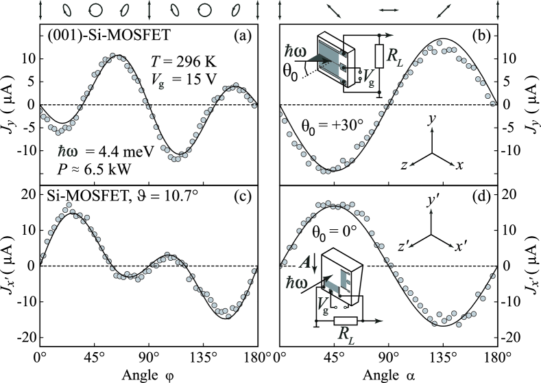
First, we discuss the polarization dependences of the photocurrent in (001)-oriented structures. Figure 1(a) shows the photocurrent measured perpendicular to the light propagation at oblique incidence of radiation in the plane for an angle . The light polarization states for several angles are sketched on the top of Fig. 1(a). Obviously the signal reverses its sign upon switching the radiation helicity from left- to right-handed circular polarization. This is the characteristic fingerprint of the circular photogalvanic effect. SturmanFridkin_book ; Ivchenko_book ; GanichevPrettl ; IvchenkoGanichev_book In addition, the photocurrent has a contribution independent of the photon helicity. The whole dependence can be well fitted by
| (4) |
with comparable parameters and . Such a dependence is in full agreement with the phenomenological Eq. (2) since the polarization dependent terms are reduced to and in this experimental geometry. Here, is the electric field amplitude of the incident light, and are the amplitude transmission coefficients for - and -polarized radiation, is the angle of refraction related to the incidence angle by with the refraction index of the medium . The first and second terms on the right-hand side of Eq. (4) correspond to the linear and circular photogalvanic effects, respectively, see Sec. II. Varying the angle of incidence from to we observed that both contributions to the photocurrent reverse their signs. Moreover, by changing the plane of incidence from to , we obtained that the photon-helicity current in the direction vanishes and only the LPGE contribution remains. All these features correspond to the phenomenological Eq. (2).
Equation (2) demonstrates that the photocurrent can also be induced by linearly polarized radiation. In this case, the signal should solely be caused by the LPGE, because the CPGE vanishes for linear polarization. The dependence of on the azimuth angle is given in Fig. 1(b) and can be well fitted by
| (5) |
with the same parameter used in Eq (4). This behavior is also expected from Eq. (2), because .
Now we turn to the transistors made on miscut surfaces. In contrast to (001)-oriented structures, here we observed a photocurrent even at normal incidence of radiation [Figs. 1(c),(d)]. This difference follows from the symmetry arguments discussed above, see Eqs. (2) and (3). The photon-helicity dependent current is detected only in the transistor along , therefore, we focus below on this particular geometry. The polarization dependences and can also be fitted by Eqs. (4) and (5), respectively, with another set of fitting parameters. They are in accordance with the phenomenological Eq. (3) since at normal incidence , , and . However, we emphasize that, in contrast to (001)-oriented structures, the photocurrent in miscut samples is determined by the crystallographic axes rather than by the light propagation direction.
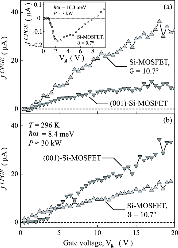
The contributions of the circular and linear photogalvanic effects persist for all applied gate voltages from to V, photon energies and temperatures used in our experiments on both types of MOSFETs. First we discuss the gate voltage dependences of the CPGE [Fig. 2(a)] and LPGE [Fig. 2(b)] contributions, i.e. and , respectively, obtained at room temperature. For the photon energy meV, as well as the most other studied wavelengths, an increase in the gate voltage results in a rise of the photocurrent magnitude. Such a behavior can be attributed to the increase in the electron density in the inversion channel and, therefore, the enhancement of the Drude absorption. However, while the LPGE contribution always increases with , the CPGE at some photon energies exhibits a sign inversion with raising , as demonstrated for the photon energy meV in the inset in Fig. 2(a). We note that we can not attribute this gate voltage to any characteristic energy in the band structure of silicon-based quantum-confined channels.
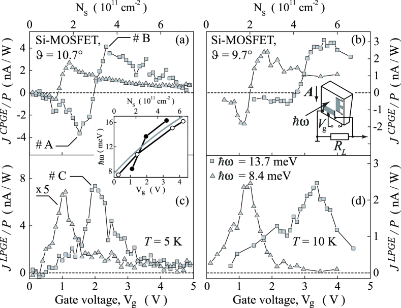
The most spectacular discrepancy in the CPGE and LPGE behavior emerges at helium temperature. While the polarization dependences remain the same, the gate voltage dependences get consistently different. In contrast to the smooth behavior observed at room temperature, at helium temperature the LPGE current exhibits a resonance-like response and the CPGE photocurrent shows always a sign inversion. This is shown in Fig. 3 for two miscut Si-MOSFETs with different angles of inclination and . The peak position of the LPGE current, which coincides with the inversion point of the CPGE, depends on the photon energy and corresponds to , where is the energy separation of the first two electron subbands. The latter is in accordance with band structure calculations Ando1 and experiments on far infrared absorption Knesch1 (see inset to Fig. 3) as well as with our photoconductivity measurements (not shown). The resonance condition is obtained by tuning the energy separation between the first two electron subbands to the photon energy by changing the gate voltage: The increase in the photon energy shifts the intersubband resonance to larger gate voltages.Stern1 The discrepancy in the resonance positions for a fixed photon energy observed in the two miscut samples is attributed to the difference of their inclination angles.
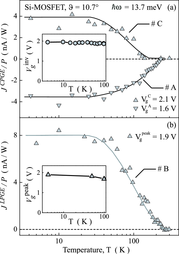
By increasing the temperature from liquid helium to room temperature the resonant peak of the LPGE and as well as the sign inversion of the CPGE at vanish. This is shown in Fig. 4 for three characteristic gate voltages: All three signals remain almost constant below about K and decrease for higher temperatures. The insets in Figs. 4(a),(b) demonstrate that the inversion point of the CPGE and the peak position of the LPGE do not shift with temperature as far as they are detectable in agreement with the behavior of well known for MOSFETs.Stern1 At K, the gate voltage dependences of the current contributions become smooth similar to those observed at room temperature.
V Microscopic theory of the CPGE
The microscopic theory of the photogalvanic effects caused by intersubband optical transitions in silicon-based low-dimensional structures was developed in Ref. [Magarill89, ]. This theory describes well the resonance behavior of the linear photogalvanic effect measured at low temperatures. The observation of the photogalvanic effects apart the intersubband resonance demonstrates that the free carrier absorption also gives rise to a polarization dependent photocurrent. Below we present the microscopic theory of the CPGE in both (001)-oriented and miscut Si-MOSFETs. As addressed above, the generation of helicity dependent photocurrents in silicon-based structures is of particular interest, because spin-related mechanisms of the CPGE are ineffective due to the vanishingly small constant of spin-orbit coupling in silicon. Therefore, less studied pure orbital mechanisms determine the current formation. We consider theoretically this process following Ref. [Tarasenko07, ] and calculate the photocurrent taking into account the peculiarity of the silicon band structure.
We remind that the electron subbands in Si structures are formed by six valleys , , , , and located at the points of the Brillouin zone of the bulk crystal. The electron dispersion in each valley is strongly anisotropic and described by two different effective masses: longitudinal and transverse with respect to the principle axis of the valley. Due to quantum confinement, only two valleys, and , are occupied at low temperatures and low electron densities in structures grown along , while the other four valleys are considerably higher in energy. The low-energy valleys are almost equivalent and can be treated independently, because the valley splitting caused by the asymmetry of the confining potential is negligible in comparison to the kinetic energy of electrons and because inter-valley scattering is much weaker than intra-valley processes.
V.1 The CPGE in (001)-oriented structures
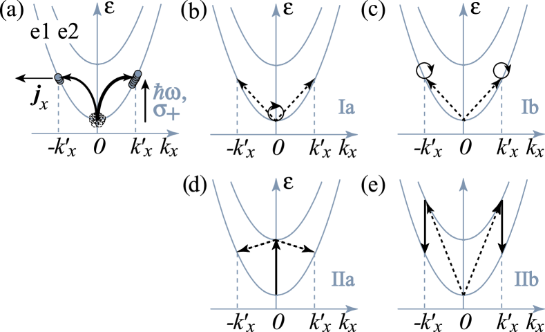
The model illustrating the generation of the photocurrent due to free-carrier absorption of circularly polarized radiation is sketched in Fig. 5. Figure 5(a) shows indirect optical transitions within the subband (we assume that only the ground subband is populated in the equilibrium). For fulfilling the conditions of energy and momentum conservation in this case, the transitions can only occur if the electron-photon interaction is accompanied by simultaneous electron scattering by phonons or static defects. Such indirect transitions are theoretically treated as second-order virtual processes via intermediate states. The intermediate states can be those within the same quantum subband as well as in other conduction or valence subbands. Figures 5(b) and (d) show possible absorption pathways with intermediate states in the subband and the excited subband .
The pathway, which is usually considered and determines the structure absorbance at normal incidence, involves intermediate states within the subband . Such transitions (path I) are shown in Figs. 5(b) and (c) for the process, where the electron-photon interaction is followed by electron scattering [Fig. 5(b)] and the inverted sequence process [Fig. 5(c)]. The matrix element of such kind of processes has the form
| (6) |
where and are the initial and final electron wave vectors, respectively, is the electron charge, the speed of light, the amplitude of the vector potential of the electromagnetic wave, which is related to the radiation intensity by , and is the matrix element of electron scattering within the subband . We note that, while the matrix element in Eq. (6) is odd in the wave vector, the absorption probability given by the squared matrix element is even in . Thus, this type of processes alone does not introduce an asymmetry in the carrier distribution in -space and, consequently, does not yield an electric current.
In the geometry of oblique incidence, which is required for the CPGE in (001)-oriented structures, additional pathways with intermediate states in the excited subbands , etc. also contribute to the radiation absorption. Such virtual transitions (path II) via states in the subband are sketched in Figs. 5(d) and (e). The matrix elements of the transitions with intermediate states in the subband () have the form Tarasenko07
| (7) |
where is the energy separation between the subbands at , the coordinate matrix element, the function of size quantization, and is the matrix element of intersubband scattering. Equation (7) shows that this type of indirect transitions is independent of and, consequently, also does not result in an electric current.
The photocurrent emerges due to quantum interference of the virtual transitions considered above. Indeed, the total probability for the real optical transition is given by the squared modulus of the sum of matrix elements describing individual pathways,
| (8) |
Beside the probabilities of individual processes, it contains interference terms. By using Eqs. (6) and (7) we derive for the last terms on the right-hand side of Eq. (8)
| (9) |
These terms are odd in the wave vector and, therefore, result in different rates for the transitions to and . This leads to an imbalance in the carrier distribution between and , i.e. to an electric current . Such a difference in real optical transition rates caused by constructive or destructive interference of various pathways is illustrated in Fig. 5(a). Moreover, it follows from Eq. (9) that the sign of the interference terms is determined by components of the vector product and, therefore, by the radiation helicity due to . Thus, the imbalance of the carrier distribution in -space and, consequently, the photocurrent reverse upon switching the light helicity.
To calculate the photocurrent we assume that electrons populate only the ground subband, they are elastically scattered by short-range defects, and . Then, making an allowance for transitions via all electron subbands, one can write for the photocurrent IvchenkoPikus_book ; Tarasenko07
| (10) |
where is the momentum relaxation time, the electron velocity in the channel plane, the electron kinetic energy measured from the subband bottom, the function of equilibrium carrier distribution in the subband , and the factor 8 in Eq. (10) accounts for the spin and valley degeneracy. For the electron scattering by short-range defects within the subband , the momentum relaxation time is given by , where the angular brackets denote averaging over the impurity distribution.
Finally, summing up Eq. (10) over the wave vectors and we derive the following expressions for components of the helicity dependent photocurrent:
| (11) |
and , where is the fine-structure constant and is the dimensional parameter, which is given by
and equal to 1 and 2 for the cases of and , respectively, with the mean kinetic energy of carriers in the equilibrium .
V.2 The CPGE in MOSFETs on miscut surfaces
In Si-MOSFETs fabricated on a miscut surface, the CPGE becomes possible even at normal incidence of radiation. This stems from the anisotropy of the electron dispersion in a valley together with the asymmetry of the confinement potential. Magarill89 ; Olbrich09 The Hamiltonian describing electron states in the channel on a miscut surface in each of the low-energy valleys has the form (see, e.g. Ref. [IvchenkoPikus_book, ])
| (12) |
where is the momentum operator, is the tensor of the reciprocal effective masses with the non-zero components , , , , and is the confining potential. The only nontrivial symmetry element, which does not change the Hamiltonian in Eq. (12) provided that , is the mirror reflection . Thus, the Hamiltonian corresponds to the point-group symmetry that allows the photocurrent in the geometry of normal incidence of radiation.
The eigen wave functions and energies of the Hamiltonian (12) are given by
| (13) |
| (14) |
where is the in-plane coordinate, is the function of size quantization at , is the energy of the bottom of the subband , and .
Similarly to the CPGE in (001)-oriented structures, the microscopic origin of the CPGE is the quantum interference of virtual optical transitions with intermediate states in the ground and excited subbands. The latter processes are possible in structures on miscut surfaces even at normal incidence of radiation due to the presence of the off-diagonal component in the Hamiltonian, which couples the motion of carriers along the and axes. The matrix elements of virtual transitions via states in the ground and excited electron subbands have the form Olbrich09
| (15) |
Finally, calculating Eq. (10) with the matrix elements of Eq. (15) and taking into account that in the case of short-range scattering, we derive
| (16) |
According to the symmetry analysis, the helicity-dependent photocurrent induced by normally-incident radiation arises to the extent of the channel plane deviation from the plane together with the channel asymmetry. This follows also from Eq. (16), which demonstrates that the current vanishes if the channel plane is parallel to , where , or for the symmetrical structure, where for any .
VI Discussion
Equations (11) and (16) describe the main features of the circular photocurrent observed in electron channels on (001)-oriented and miscut silicon surfaces. In fact, it follows from Eq. (11) that the CPGE in the (001)-oriented structure can occur only at oblique incidence and in the direction normal to the incidence plane. By contrast, in miscut structures, the circular photocurrent along can be excited even at normal incidence [see Eq. (16)]. Such a behavior of the CPGE in respect to the light propagation direction and crystallographic orientation has indeed been observed in all samples under study.
The microscopic origin of the circular photocurrent reversal upon variation of the energy separation between the subbands from to can be also clarified from Eqs. (11) and (16). In the vicinity of the intersubband resonance, the spectral dependence of the photocurrent is given by , which stems from the matrix elements describing virtual transitions via the excited subbands, see Eqs. (7) and (15). Thus, the photocurrent should increase drastically and undergo spectral inversion at . In experiment, the resonant condition is obtained by tuning the intersubband separation with the gate voltage while the photon energy is fixed. Since at low temperatures only the ground subband is populated, the photocurrent inversion upon variation of is observed for , see Fig. 1. While Eqs. (11) and (16) yield sharp spectral resonances, in real structures the dependence smooths because of broadening, but the inversion remains.
The magnitude of the CPGE detected in the transistor on the miscut surface with for meV and = 3 V is nA/W, yielding the current density nA cm/W. The same order of magnitude is obtained from Eq. (16) for the structure with the miscut angle , the carrier density cm-2 (= 3 V), the channel width nm and the structure asymmetry degree .
In deriving Eqs. (11) and (16) we considered the intrasubband optical transitions within the ground subband assuming that the momentum relaxation time is independent of the electron energy. Such an approximation is reasonable when the kinetic energy of photoexcited carriers is smaller than . For electrons generated with the energy the momentum relaxation time gets shorter due to the additional relaxation channel caused by intersubband scattering. Consequently, one can expect that the magnitude of the CPGE current is smaller at (low ) than that at (high ). This can be responsible for the observed asymmetry in the gate voltage dependence of the photocurrent in the vicinity of the intersubband resonance, see Fig. 3. The gate voltage changes also the channel profile, which can be taken into account assuming that the ratios and the coordinate matrix elements depend on . At , possible contributions to the CPGE due to intersubband optical transitions as well as scattering-induced broadening of the absorption peak should also be considered. Magarill89
With increasing temperature the intersubband resonances are broadened and the excited subbands , etc. become also occupied in the equilibrium. It leads to additional channels of the current formation including those with initial states in the excited subbands. As a result, both resonant LPGE and CPGE at drastically decrease with temperature (see Fig. 4), and the spectral behavior of the photocurrent becomes more complicated. We observe that at room temperature the CPGE current inversion with the gate voltage is detected only for the photon energy meV. Moreover, even in this case, the point of inversion does not correspond to .
VII Summary
In conclusion, we have studied the circular and linear photogalvanic effects in Si-MOSFETs under excitation with linearly and elliptically polarized radiation in the terahertz frequency range. The behavior of photogalvanic effects upon variation of the radiation polarization state, wavelength, temperature and bias voltage have been investigated in transistors prepared on (001) precisely oriented as well as on miscut surfaces. The observed polarization properties of the photocurrent are well described by the phenomenological theory of the photogalvanic effects based on symmetry analysis of the studied structures. Our experiments on Si-based structures reveal that the photon-helicity dependent photocurrents can be generated in low-dimensional semiconductors even with negligible spin-orbit interaction. The mechanism of the photocurrent formation is based on the quantum interference of different pathways contributing to the radiation absorption. The microscopic theory of the circular photogalvanic effect under intrasubband (Drude-like) absorption in the ground electron subband has been developed being in a good agreement with the experimental findings.
Acknowledgements.
We thank E.L. Ivchenko, V.V. Bel’kov, and J. Kamann for helpful discussions. The financial support from the DFG, the Linkage Grant of IB of BMBF at DLR, and the RFBF is gratefully acknowledged. S.A.T acknowledges also the support from the Russian President Grant for young scientists (MD-1717.2009.2).References
- (1) B.I. Sturman and V.M. Fridkin, The Photovoltaic and Photorefractive Effects in Non-Centrosymmetric Materials (Nauka, Moscow, 1992; Gordon and Breach, New York, 1992).
- (2) E.L. Ivchenko, Optical spectroscopy of semiconductor nanostructures (Alpha Science Int., Harrow, UK, 2005).
- (3) S.D. Ganichev and W. Prettl, Intense Terahertz Excitation of Semiconductors (Oxford University Press, Oxford, 2006).
- (4) E.L. Ivchenko and S.D. Ganichev, Spin Photogalvanics in Spin Physics in Semiconductors, ed. M.I. Dyakonov, (Springer, Berlin, 2008).
- (5) S.N. Danilov, B. Wittmann, P. Olbrich, W. Eder, W. Prettl, L.E. Golub, E.V. Beregulin, Z.D. Kvon, N.N. Mikhailov, S.A. Dvoretsky, V.A. Shalygin, N.Q. Vinh, A.F.G. van der Meer, B. Murdin, and S.D. Ganichev, J. Appl. Physics 105, 013106 (2009).
- (6) L.I. Magarill and M.V. Entin, Sov. Phys. Solid State 31, 1299 (1989).
- (7) E.L. Ivchenko and G.E. Pikus, Superlattices and Other Heterostructures (Springer-Verlag, Berlin, 1997).
- (8) S.A. Tarasenko, JETP Lett. 85, 182 (2007).
- (9) G.M. Gusev, Z.D. Kvon, L.I. Magarill, A.M. Palkin, V.I. Sozinov, O.A. Shegai, and V.M. Entin, JETP Lett. 46, 33 (1987).
- (10) P. Olbrich, S.A. Tarasenko, C. Reitmaier, J. Karch, D. Plohmann, Z.D. Kvon, and S.D. Ganichev, Phys. Rev. B 79, 121302(R) (2009).
- (11) W. Knap, M. Dyakonov, D. Coquillat, F. Teppe, N. Dyakonova, J. Lusakowski, K. Karpierz, M. Sakowicz, G. Valusis, D. Seliuta, I. Kasalynas, A. El Fatimy, Y.M. Meziani, and T. Otsuji, J. Infrared Millimeter Terahertz Waves 30, 1319 (2009).
- (12) S.D. Ganichev, E.L. Ivchenko, S.N. Danilov, J. Eroms, W. Wegscheider, D. Weiss, and W. Prettl, Phys. Rev. Lett. 86, 4358 (2001).
- (13) S.D. Ganichev and W. Prettl, J. Phys.: Condens. Matter, 15, R935 (2003).
- (14) M. Bieler, N. Laman, H.M. van Driel, and A.L. Smirl, Apl. Phys. Lett. 86, 061102 (2005).
- (15) T. Ando, Z. Phys. B 26, 263 (1977).
- (16) P. Kneschaurek, A. Kamgar, and J.F. Koch, Phys. Rev. B 14, 1610 (1976).
- (17) T. Ando, A.B. Fowler, and F. Stern, Rev. Mod. Phys. 54, 437 (1982).