Atomic and electronic structure of monolayer graphene on -SiC : a scanning tunneling microscopy study.
Abstract
We present an investigation of the atomic and electronic structure of graphene monolayer islands on the -SiC (SiC) surface reconstruction using scanning tunneling microscopy (STM) and spectroscopy (STS). The orientation of the graphene lattice changes from one island to the other. In the STM images, this rotational disorder gives rise to various superlattices with periods in the nm range. We show that those superlattices are moiré patterns (MPs) and we correlate their apparent height with the stacking at the graphene/SiC interface. The contrast of the MP in STM images corresponds to a small topographic modulation (by typically 0.2 Å) of the graphene layer. From STS measurements we find that the substrate surface presents a eV wide bandgap encompassing the Fermi level. This substrate surface bandgap subsists below the graphene plane. The tunneling spectra are spatially homogeneous on the islands within the substrate surface gap, which shows that the MPs do not impact the low energy electronic structure of graphene. We conclude that the SiC reconstruction efficiently passivates the substrate surface and that the properties of the graphene layer which grows on top of it should be similar to those of the ideal material.
pacs:
68.37.Ef, 68.35.bg, 73.20.AtI Introduction
Fascinating properties have been predicted and observed for monolayer grapheneGeim and Novoselov (2007); Castro Neto et al. (2009). Among them one finds the anomalous quantum Hall effectNovoselov et al. (2005); Zhang et al. (2005), the Klein tunneling phenomenonKatsnelson et al. (2006); Young and Kim (2009), and weak (anti)localization effectsWu et al. (2007); McCann et al. (2006). Moreover, suspended graphene shows exceptionally high carriers mobilityBolotin et al. (2008a); Du et al. (2008) even near room temperatureBolotin et al. (2008b). These features make graphene an attractive material for the investigation of original physical phenomenaCheianov et al. (2007); Ponomarenko et al. (2008) and for the development of devices such as transistorsNovoselov et al. (2004); Meric et al. (2008) and captorsSchedin et al. (2007).
The physical properties of free standing graphene are intimately linked to the presence of two equivalent carbon sublattices commonly called A and B. Usually, graphene layers are supported on a substrate and the interaction between the electronic states of the substrate surface and the orbitals of the C atoms can significantly alter the electronic structure -and thus the properties- of the material. This has been shown recently by angle resolved photoemission for graphene elaborated on metal surfaces where this coupling modifies the band dispersion close to the Dirac pointGrüneis and Vyalikh (2008); Brugger et al. (2009); Sutter et al. (2009a), suppressing the “Dirac cones”. The investigation of the atomic and electronic structure of the interface between graphene and the substrate is thus of primary importance. This is in particular the case for few layers graphene grown on SiC substrates, where as-grown samples are used for physical measurements Berger et al. (2004, 2006); Wu et al. (2007); de Heer et al. (2007), since the doped graphene layers close to the interface should give the largest contribution to electrical transportBerger et al. (2006).
Few layers graphene are obtained by high temperature treatment of the polar faces of SiC substrates van Bommel et al. (1975); Forbeaux et al. (1998, 1999). Usually commercial hexagonal ( or ) substrates are used. They have two different faces, the one (the Si face) and the faces (the C face). The interface between the Si face and the graphene overlayer has been extensively studied in the last few years. The current model for this interface is that the first graphitic layer strongly interacts with the substrate, giving rise to the () reconstructionKim et al. (2008); Varchon et al. (2008a). Covalent bonds form between Si atoms of the substrate surface and the graphene layer, which results in the suppression of the Dirac cones characteristic of graphene Mattausch and Pankratov (2007); Varchon et al. (2007); Kim et al. (2008). This model is supported by photoemission dataEmtsev et al. (2008). Accordingly no graphene contrast has been detected in STM images of the reconstructionMallet et al. (2007); Riedl et al. (2007); Rutter et al. (2007); Lauffer et al. (2008), which is usually called the “buffer layer”. The electronic structure of graphene is developed only for the second C planeKim et al. (2008); Varchon et al. (2008a); Varchon et al. (2007); Mattausch and Pankratov (2007), where a band structure very similar to the Dirac cones has been observed experimentallyBostwick et al. (2007); Zhou et al. (2007). The question of a possible perturbation of the electronic structure of the graphene layer due to an interaction with the buffer layer remains openRotenberg et al. (2008); Zhou et al. (2008). Nevertheless, the honeycomb contrast expected for ideal graphene is observed by STM on this second C planeMallet et al. (2007); Rutter et al. (2007); Lauffer et al. (2008); Brar et al. (2007). Moreover the analysis of the standing wave patterns indicates that the electronic chirality of graphene is preservedBrihuega et al. (2008).
The interface between graphene and the C face has been less extensively studied. It has long been known that the growth is quite different on the C and the Si facevan Bommel et al. (1975). Graphitic films grown in UHV conditions on the C face exhibit some rotational disordervan Bommel et al. (1975); Forbeaux et al. (1999). This disorder already exists for the first C layerEmtsev et al. (2008); Hiebel et al. (2008); Starke and Riedl (2009). Interestingly, it was found using photoemission that the interaction between the first C layer and the substrate was much weaker than for the Si face: no buffer layer is detected in core level spectroscopyStarke and Riedl (2009); Emtsev et al. (2008) and the band structure of this layerEmtsev et al. (2008) resembles the one of graphene. The situation is however complicated by the facts that i) two different pristine reconstructions of the substrate -the SiC and the SiC- exist at the interface below the graphene layerStarke and Riedl (2009); Emtsev et al. (2008); Hiebel et al. (2008) and ii) that several orientations exist for the graphene islands for each reconstruction, leading to different superlatticesHiebel et al. (2008). A systematic analysis of the interface for the two different substrate reconstructions aiming at understanding their atomic and electronic structure for the different orientations of the graphene layer is thus needed. This is best achieved by STM, which can address each individual island.
In a previous paper we have shown that a graphitic signal could be observed at low bias for both the SiC and the SiC reconstructions, indicating a weaker coupling with the substrate than on the Si faceHiebel et al. (2008). A recent ab-initio calculation has shown that the reduced interaction in the case of the SiC reconstruction is due to a passivation of the substrate surface by Si adatomsMagaud et al. (2009). The linear dispersion of the graphene bands close to the Dirac point is preserved, but a residual coupling with the substrate, also evidenced by STM, was found. In the present paper we concentrate on the graphene islands formed on the SiC interface reconstruction, which are called islands afterward, where the interaction with the substrate seems to be even smallerHiebel et al. (2008). We first analyze the geometric structure of the superlattices. We show that they are moiré patterns and we relate their apparent height to the local stacking at the interface. We then analyze the electronic structure of the islands compared to that of the bare substrate SiC reconstruction. A wide surface bandgap (of width eV) is found by STS in the electronic structure of the bare reconstruction, which persists below the graphene layer. The Fermi level of graphene is located in the vicinity of the top of this surface gap. In STM images a graphene signal dominates inside the substrate surface gap, and the STS data explain the high bias “transparency” of graphene. A comparison between STM images of islands for a specific orientation with previous ab-initio calculations -as well as with the case of the Si face- indicates that the substrate reconstruction is responsible for the weak graphene-substrate interaction. Finally we show that the moiré pattern is essentially of topographic origin. It is associated with small undulations of the graphene layer. From STS, these undulations do not lead to heterogeneities in the electronic structure of graphene, at variance with the case of more strongly interacting systems such as graphene on Ru(0001)Vázquez de Parga et al. (2008). From these data we conclude that the islands should be a system close to ideal, uncoupled, graphene. At present it is not clear whether the structure is present at the interface for few layers graphene films elaborated at high temperature in non UHV conditionsHass et al. (2007). Our results indicate anyway that manipulating the atomic structure of the surface can be a useful way to modify the coupling at the interface, as shown previously for metal substratesVarykhalov et al. (2008).
II Experiment
The sample preparation and characterization were conducted under ultrahigh vacuum. The sample graphitization was performed in-situ by following the procedure presented previouslyHiebel et al. (2008). The n doped -SiC samples were first cleaned by annealing under a Si flux at C. The already reported SiC reconstructionHoster et al. (1997) was obtained by further annealing at C. After annealing steps at increasing temperature, a graphene coverage of less than a monolayer is finally detected by low energy electron diffraction (LEED) and Auger spectroscopy. At this stage, the LEED patterns show SiC and SiC spots and a ring-shaped graphitic signal with modulated intensityEmtsev et al. (2008); Hiebel et al. (2008); Starke and Riedl (2009).
The STM and STS measurements were made at room temperature with mechanically cut PtIr tips. 5 samples were investigated, using more than 10 macroscopically different tips. The samples morphology observed by STM was similar to previous results, with the presence of bare SiC reconstructed substrate domains, graphene monolayer islands on the SiC reconstruction (G_) and on the SiC reconstruction (G_) and also few multilayer islandsHiebel et al. (2008); Starke and Riedl (2009). The focus of this paper is the structure of G_ islands and several dozens of them were observed.
III Results and discussion
III.1 Superlattices and local stacking of monolayer graphene on the SiC reconstruction
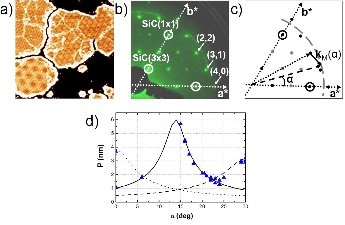
STM images show that islands present superlattices (SLs) of various periodicities in the nanometer range (see Fig. 1 (a)). Contrary to graphene on SiC (Si face), graphene on SiC (C face) exhibits a significant rotational disorder, already from the first graphene layer. This results in a ring-shaped graphitic signal on LEED patterns (Fig. 1 (b)). A previous STM study established that the SL period depends on the orientation angle of the graphene layer with respect to the substrate surface lattice Hiebel et al. (2008). In this section we present a more quantitative analysis of the SLs that identifies them as moiré patterns (MPs).
Moiré patterns arise from a non linear composition of two periodic latticesAmidror (1999). They appear as an additional periodic lattice of larger period than the two components. For example, MPs are observed by STM on graphitePong and Durkan (2005) and few layer graphene samples with rotational stacking faultsVarchon et al. (2008b). They also show up when two lattices of different lattice parameters are superimposed as for graphene monolayer on transition metalsN’Diaye et al. (2008); Vázquez de Parga et al. (2008); Marchini et al. (2007). For two periodic lattices with reciprocal lattice vector and respectively, the resulting MP is characterized by the reciprocal lattice vectorAmidror (1999); N’Diaye et al. (2008):
| (1) |
In the system we consider, the SiC lattice parameter being almost 4 times bigger than the one of graphene, high order spectral components have to be considered. As we can see on the LEED pattern in Fig. 1 (b), first order SiC spots are located far away from the graphitic signal. According to equation (1), moiré patterns constructed on these spots and any graphene spot would have a smaller period than the SiC lattice, which cannot explain the observed SLs. SiC spots can also be ruled out for similar reasons. From the LEED pattern of fig. 1 b), the reciprocal lattice vectors of the SiC reconstruction most likely to lead to MPs with periods in the nanometer range are the high order , , ones and their symmetric counterparts in the reciprocal space. Fig. 1 (c) provides an illustration of a MP construction associated to the SiC spot of the LEED pattern, for a graphene island of orientation with respect to the SiC surface lattice.
Thus, we calculated the moiré periodicity as a function of the graphene orientation angle with respect to the SiC surface lattice with ranging from to (due to the symmetry of the system seen on the LEED pattern). For each of the three relevant SiC Fourier components, we use equation (1) and . The three resulting curves are plotted in Fig. 1 (d). We have also measured moiré periodicities versus graphene orientation angles on STM images of monolayer islands (such as Fig. 1 (a)), with an accuracy of nm and respectively. As represented on Fig. 1 (d) , experimental data do fit very well with calculations. For a given angle, the largest period - which corresponds to the best match in reciprocal space - is generally predominant in the images. We also note that most studied islands exhibit an orientation angle between and . This is consistent with the peculiar rotation angle distribution revealed by LEEDHiebel et al. (2008); Starke and Riedl (2009). We will thus concentrate on these orientations in the following. To summarize, we interpret superlattices on monolayer islands as high order MPs, resulting from the superposition of the SiC and the graphene-like lattices. Note however that the moiré interpretation is essentially geometric and that it does not give any information on the nature of the interaction between graphene and its substrate. We shall consider this point in section III.3.
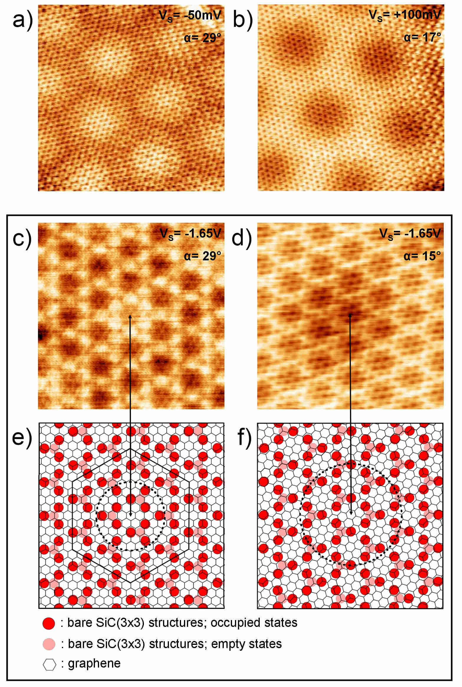
We now focus on the atomic structure and on the stacking for graphene islands with a MP constructed on the and SiC Fourier components which are the most common on our samples (). As shown on Fig. 1 (d), the corresponding moiré periodicity is maximum for a graphene orientation angle of and respectively. Low bias STM images (see Fig. 2 (a), (b)) show that the MPs observed for angles close to these two values exhibit inverted contrasts: “ball-like” for close to , “hole-like” for close to . At the atomic scale, a well defined honeycomb pattern characteristic of monolayer graphene is observed at low bias for both orientations (see Fig. 2 (a), (b)). We point out that the moiré contrast on islands shows no variations with the tip and tunneling conditions: bright areas remain bright at any bias and for all tips tested (see Fig. 5).
In order to understand the variation of the MP contrast with angle , we studied the local stacking of the graphene and SiC lattices for close to and . As already mentioned in previous papersRiedl et al. (2007); Mallet et al. (2007); Hiebel et al. (2008); Rutter et al. (2007), graphene appears transparent on high bias STM images so that the interface -the SiC reconstruction in the present case- becomes visible. Conversely, atomic resolution on graphene is obtained on low bias images. Thus, stacking can be observed using two different approaches: by dual bias imaging at low and high bias or by imaging at an intermediate tunnel bias voltage, which corresponds to a crossover between these two extreme situations (to be discussed in section III.2). The latter type of image is represented in Fig. 2(c) and 2(d) for islands with and respectively. For this sample bias ( V), the graphene and SiC lattices appear simultaneously. Schematic reproductions of the images in Fig. 2(e) and (f) give a clear view of the local stacking (the same result is found from dual bias imaging). Since no established structure model for the SiC reconstruction exist, we represent in Fig. 2 (e), (f) the states detected by STM on the substrate surfaceHoster et al. (1997): filled (empty) states are represented in red (light-red) (dark gray and light gray in the printed version).
In the case (Fig 2 (e)), the graphene and SiC lattices are quasi commensurate. The corresponding common Wigner-Seitz cell is represented by solid lines. The apparent height of the MP is maximum in the center of the cell and minimum on its edges. These areas correspond to two different types of stacking. At the center of the cell (circled area), SiC states are located under the center of graphene hexagons (i.e. no C atom is in coincidence with SiC states). On the edges (dark area), all SiC states have C atoms or C-C bonds on top of them.
In the case, the moiré corrugation is inverted. The apparent height of the moiré is minimal at the center of the cell and maximal at its edges. Now the stacking at the center of the cell (circled area) is such that every SiC state has C atoms or C-C bonds directly above which is similar to the stacking in the dark area of the case. At the edges of the cell, a significant amount of SiC states are located under the center of graphene hexagons, as for the bright regions in the case. Therefore, the local stacking of bright (high) and dark (low) areas is the same for the two kinds of MP contrast, “ball-like” () and “ hole-like” (). The apparent MP “contrast inversion” arises from changes in the local stacking induced by the graphene rotation.
Islands with deserve particular attention because they allow a direct comparison with the experimental results for the Si face and with theoretical calculations. For , the graphene and the SiC lattices are (quasi)-commensurate with a -SiC () common cell (or a graphene cell). This is the configuration which is observed for the Si facevan Bommel et al. (1975); Forbeaux et al. (1998); Tsai et al. (1992), the layer orientation is imposed by the substrate and is therefore the same on the whole sample. A strong interaction between the first graphitic layer (“buffer layer”) and the substrate occurs so that only the second layer shows graphene properties Varchon et al. (2007); Kim et al. (2008); Varchon et al. (2008a); Mattausch and Pankratov (2007). In particular, no honeycomb contrast characteristic of graphene has ever been observed in STM studies of the phase of the Si face -corresponding to the first graphitic layer or “buffer layer”- since it lacks states in the vicinity of the Fermi levelEmtsev et al. (2008). Additionally, this usually gives rise to a dominant SiC superstructure in STM imagesTsai et al. (1992), although high resolution images reveal the actual periodicityRiedl et al. (2007).
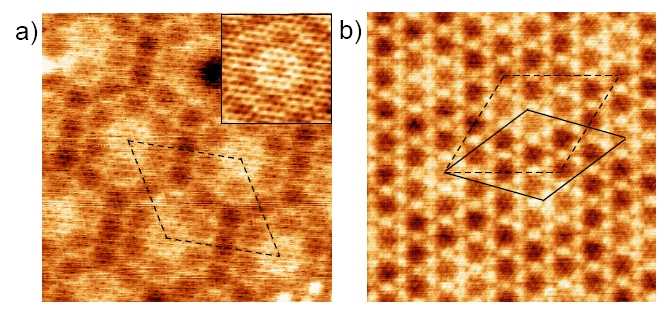
A totally different situation occurs for graphene on the SiC reconstruction of the C face. For , Fig. 3 (a), we actually observe a with respect to the SiC, which corresponds to the actual (and not SiC) superstructure with respect to the SiC . More important, the honeycomb contrast of graphene clearly shows up at low bias (see inset in Fig. 3). This demonstrates that the graphene states are present close to the Fermi level and thus implies a comparatively much weaker interaction with the substrate compared to the Si face. This weak coupling probably results from the presence of the SiC surface reconstruction below the graphene layer. Indeed, ab-initio calculations performed for a graphitic C layer on the ideal (non-reconstructed) C face for this orientation () indicate a strong bonding to the substrateVarchon et al. (2007); Varchon et al. (2008a); Mattausch and Pankratov (2007) and subsequently the disappearance of the states at low energy, as for the Si face. This suggests that the SiC reconstruction efficiently passivates the substrate surface for the C face, preventing the formation of chemical bonds with the graphene layer. Similar results were obtained from ab-initio calculations for graphene monolayer on the SiC reconstructionMagaud et al. (2009), a system that coexists with on the SiC graphitized surface.
Another observation we have made on islands for is that the orientation of the graphene layer is not locked to . To see that, we took advantage of the fact that the MP orientation with respect to the SiC lattice is highly sensitive to the rotation angle . Indeed, for a change by of , the orientation of the MP changes by (for ). Thus, we could identify some slight deviations () from the quasi-commensurate () configuration. Fig. 3 (b) provides an illustration of this effect: the MP significantly differs from the supercell although remains close to (we measure ). The fact that such islands exist suggests that the (quasi-commensurate) configuration does not lead to a notable energy reduction, at variance with the case of the Si face. This is consistent with the absence of covalent, directional bonds between graphene and substrate at the interface for islands.
III.2 Electronic structure of monolayer graphene on the SiC reconstruction
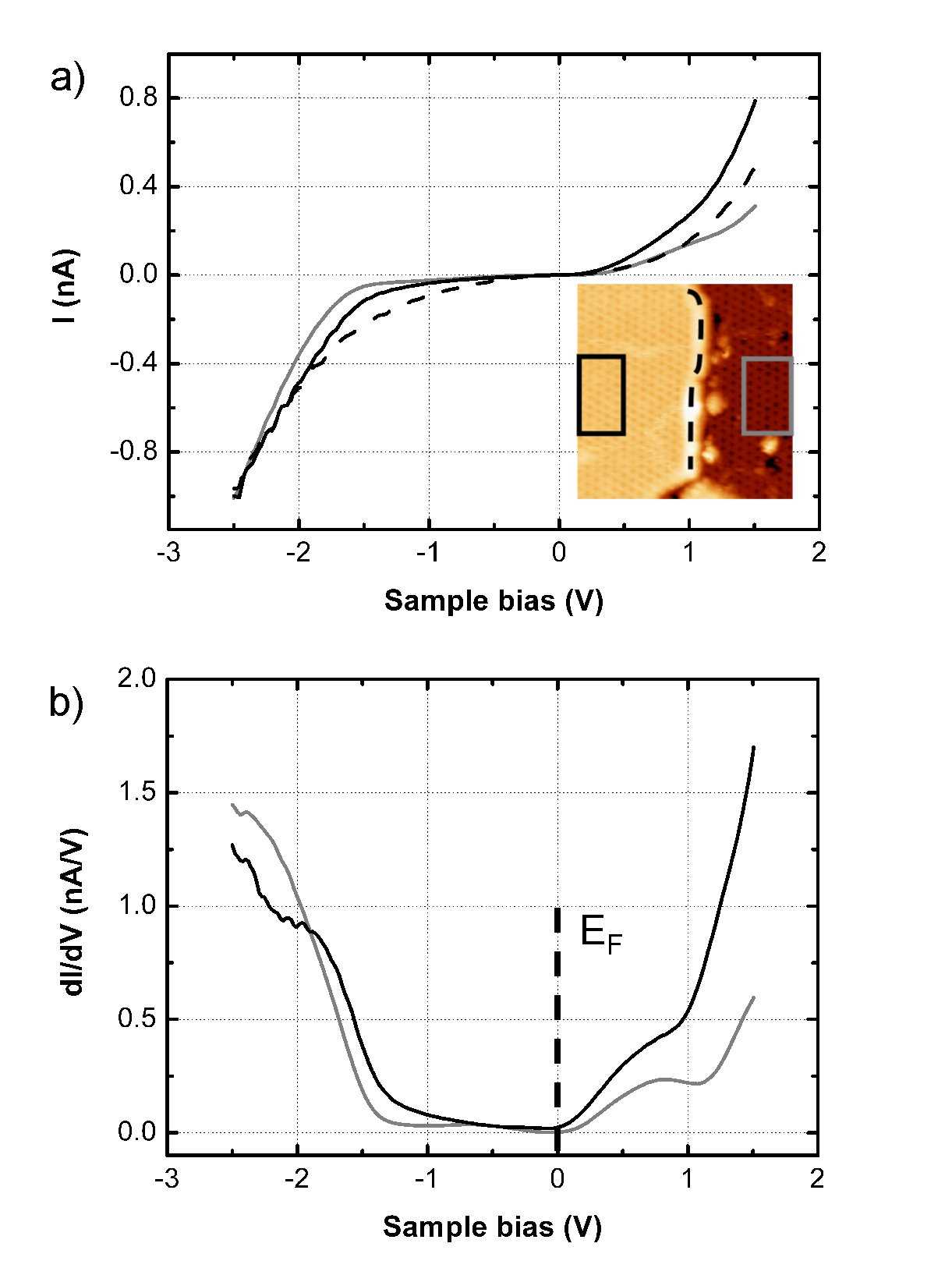
After these mainly structural considerations, we focus on the electronic structure of the graphene overlayer and of the SiC reconstruction. We first compare the electronic structure of the and SiC phases using current imaging tunneling spectroscopy (CITS). This technique consists in acquiring a constant current image and an I(V) curve after each of its points. For each spectrum, the feedback loop is turned off and the sample voltage () is ramped between preset values. I(V) curves are then numerically differentiated to get dI/dV conductance curves which are -in first approximation- proportional to the local density of states (LDOS) of the sample surface. In Fig. 4, we present CITS data acquired on a region (see insert in Fig. 4 (a)) with the bare SiC reconstructed substrate surface (right) and a island (left), so that both region are probed with the same tip. Fig. 4 (a) shows three I(V) curves, one for each type of surface, spatially averaged over the boxed regions (300 points each), and one for the edge of the graphene island (averaged over 15 points). The dI/dV spectra for the island and the bare substrate are given in Fig. 4 (b).
For the bare SiC reconstruction, the I(V) curve in Fig. 4 (a) displays a dramatic reduction of the current between V and V. This feature is still visible -although less marked- in the I(V) curve for the graphene island. The curve obtains on the edge of the island indicates that the lack of current at low bias does not arise from the electronic structure of the tip. These observations suggest the presence of a surface bandgap associated to the SiC reconstruction that subsists under the graphene layer. However, a residual current related to in-gap states is detected in the surface gap of the bare SiC reconstruction (between V and V). To further study the electronic structure of the island and of the bare substrate, the conductance curves presented in Fig. 4 (b) are analysed in the following.
The SiC spectrum exhibits a region of minimum conductance ranging from V to V. These values are only weakly dependent (within V) of the tip and sample. Hence, the SiC reconstruction presents an asymmetric surface bandgap, with the Fermi level close to the bottom of the conduction band, as expected for a n-type semiconductor. A broad structure centered around V is also detected. It is ascribed to in-gap states. An additional CITS study of the SiC reconstruction suggests that they arise from a subsurface atomic layer (not shown). For the occupied states, these observations are consistent with Angle Resolved Photoemission Spectroscopy (ARPES) dataEmtsev et al. (2008) of the bare and lightly graphitized SiC surface where a large intensity for binding energies larger than eV and a residual emission between eV and eV binding energies are detected.
The spectrum has similarities with the SiC spectrum. In particular, the structure at V (above the top of the substrate surface gap) and the rapid increase of conductance below the bottom of the substrate surface gap ( V) are clearly observed. These structures arise from the underlying SiC reconstruction. The Fermi level of graphene ( in Fig.4 (c)) is located close to the top of the substrate surface gap. Inside the SiC surface bandgap, an additional - though rather small - density of states originating from the graphene layer is detected. In other words, outside the (bare) SiC surface bandgap, the signal is dominated by the contribution of the substrate which explains the transparency of graphene at high biasRiedl et al. (2007); Mallet et al. (2007); Hiebel et al. (2008); Rutter et al. (2007).
Note that the surface bandgap of the substrate remains unchanged below the graphene layer. This again suggests a weak graphene - substrate interaction since strong coupling would also affect the electronic states of the SiC reconstruction. Moreover, for an extended energy range within the surface bandgap (from eV to eV) the density of interface states susceptible to interact with graphene states is quite small (from Fig. 4). This is consistent with graphene-like atomic contrast on low bias STM images presented here (Fig. 2) and in previous papers Hiebel et al. (2008). Nevertheless, moiré patterns are still visible on the graphene islands at energies within the SiC surface bandgap. This gives evidence for a residual effect of the substrate. Following experiments aim at discriminating between a topographic or an electronic effect for the MP contrast.
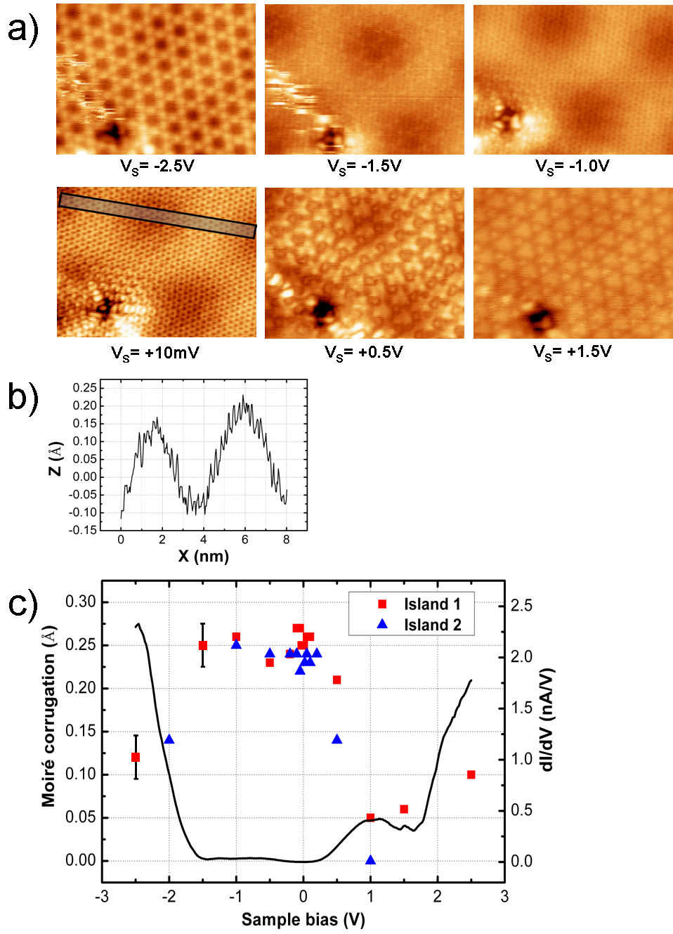
In Fig. 5 (a) we present a series of STM images of the same area of a island with at various sample bias voltages. At V, the SiC reconstruction is clearly visible while no evident graphene signal is detected. At V, atomic resolution on graphene appears, superimposed to the SiC signal as in Fig. 2(c), 2(d) and 3. For lower biases, typically from V to V, we detect a well defined honeycomb graphene signal and no more signal of the underlying reconstructioncon (see V and mV panels). From V to higher biases, no more evident graphene signal is visible and the SiC signal reappears. Thus, atomic resolution on graphene is mostly achieved within the SiC surface bandgap, as expected since the DOS arising from the SiC is small within the surface bandgap. If we now concentrate on the moiré pattern - the signal with period nm in the images of Fig. 5 (a) - we notice that its corrugation is obviously much smaller at high biases than at low biases.
To complete these observations, we have measured the peak-to-peak moiré corrugation amplitude as a function of the sample bias voltage (see graph in Fig. 5 (c)) using two different methods: i) profiles laterally averaged over 0.6nm on raw images or ii) profiles taken on low-pass filtered images in order to get rid of the high frequency atomic corrugation. Both methods gave the same results. The former method is illustrated in Fig. 5 (b) for a profile taken on the low bias image ( mV) of Fig. 5 (a). We stress that the measurements reported in Fig. 5 (c) were actually made at several spots on larger images. The uncertainty in the measurement is estimated to be of Å . It results from the residual contribution of the atomic corrugation (SiC at high bias or graphene at low bias as in Fig. 5 (b)) and to some inhomogeneities in the corrugation of the moiré patterns. The data presented in Fig. 5 (b) were acquired with different tips on two different islands (labeled “Island 1” and “Island 2”) of approximately the same orientation: , nm (STM images in Fig. 5 (a) were obtained on “Island 1”). A typical SiC average spectrum is also given on the graph in order to locate the substrate surface bandgap. The behavior is similar for both set of measurements with the following characteristics: within the SiC surface bandgap, the moiré corrugation amplitude is constant and equal to Å. Outside the surface bandgap, when the SiC contribution to the tunneling current becomes dominant, the corrugation dramatically decreases -or even vanishes. Other islands with different orientations (including angles close to ) show similar behavior of the moiré corrugation as a function of bias. These observations imply that the moiré corrugation is associated to the graphene layer and not to the SiC reconstructionmoi . Moreover, since the corrugation is independent of the bias in a large voltage range spanning the SiC surface bandgap, it is most probably of topographic origin. The corrugation amplitude varies with the moiré period, between Å and Å (smaller corrugations correspond to moiré patterns of smaller periods).
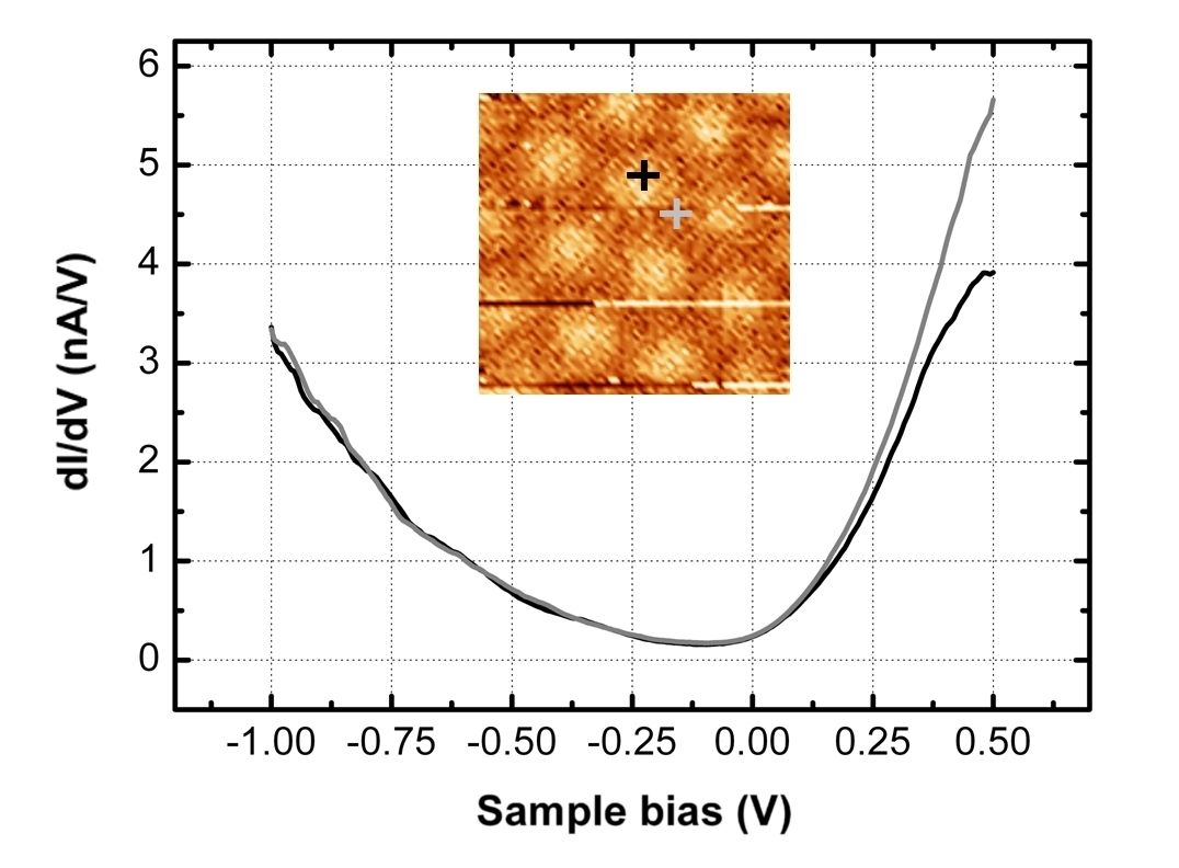
From the above observations, the graphene-substrate distance changes by Å from the highest to the lowest areas of the moiré pattern. To look for a possible change in the electronic properties correlated to these soft “ripples”, we have performed scanning tunneling spectroscopy on several islands. In Fig. 6 we present CITS results on a island with (see insert) - similar results were obtained for other values of between an . The setpoint was chosen within the substrate surface bandgap ( V) with a setpoint current of nA in order to probe essentially the graphene states. The graph shows two spectra, one corresponding to the highest regions of the moiré pattern and the other to lowest regions. Both are averaged over 24 points. The spectra coincide from V to V. This demonstrates that the electronic structure of the graphene overlayer is homogeneous and thus not affected by the moiré pattern in a wide energy range spanning the Fermi level (and located in the substrate surface bandgap). Note however that the spectroscopy measurements are conducted at room temperature and the energy resolution is thus limited to eVPons et al. (2003). From V to V, more signal is detected on the low regions than on the high ones. This discrepancy arises from topographic effects (decrease in MP corrugation) discussed in connection with Fig. 5.
Another important question is the position of the Dirac point. Previous ARPESEmtsev et al. (2008) and transport measurementsBerger et al. (2006) assess that it is located 0.2 eV below the Fermi level. But these techniques are non-local and give therefore an average value of the doping of the graphene layer. Importantly, the underlying reconstruction of the substrate is not identified in the probed region. STS is thus in principle the most adapted technique for answering this question. In Fig. 6, we find a rather structureless spectrum with a “flat” minimum ranging from V to V. Some other spectra showed a well defined minimum located around V. However, due to a significant variability in our measurements of the dI/dV curves between V and V, we refrain from giving a definite value for the position of the Dirac point.
III.3 Graphene on -SiC: an almost ideal graphene layer?
From measurements presented in Fig. 5, we find a topographic corrugation of Å to Å of the graphene monolayer while no long range topographic modulations were observed on the bare SiC reconstruction. The period of the graphene topographic modulation is related to its orientation with respect to the substrate reconstruction and follows a moiré model (discussed in connection with Fig.1). This means that the graphene corrugation is induced by the SiC reconstruction. More precisely, the graphene - substrate distance is governed by the local stacking of the SiC and the graphene overlayer as shown in section III.1.
Such an effect has already been reported for graphene on transition metals. It is instructive to compare our data with a well documented case of a relatively strong coupling, such as graphene on Ru, where the bands of graphene are strongly perturbed by interaction with the substrateBrugger et al. (2009); Sutter et al. (2009a). This system presents a moiré pattern ( nm) caused by the lattice mismatch between graphene and Ru. A signal with the periodicity of graphene is observed by STM Vázquez de Parga et al. (2008); Marchini et al. (2007) but the contrast changes from honeycomb in the high region to triangular in the low areasVázquez de Parga et al. (2008); Marchini et al. (2007); Sutter et al. (2009b). This is at variance with the uniform honeycomb pattern we observe on . DFT calculations Wang et al. (2008a), surface X-ray diffractionMartoccia et al. (2008), STMVázquez de Parga et al. (2008); Sutter et al. (2009b) and core level spectroscopy Preobrajenski et al. (2008) conclude that lower areas of the graphene layer strongly bond to the substrate.
STS results presented for graphene on Ru in Ref. Vázquez de Parga et al., 2008 are of particular relevance for the purpose of our study. It shows dI/dV spectra with significant spatial variations correlated to the moiré pattern. This finding was interpreted in Ref. Vázquez de Parga et al., 2008 using a generic model where a periodic potential -with the periodicity of the MP- is applied to a flat and isolated graphene layer. This leads to the LDOS modulations observed by STM, which also corresponds to charge inhomogeneities in the graphene layer. In Ref. Wang et al., 2008b, it was inferred from DFT calculations that the spatial variations of the STS spectra should be attributed to the spatially heterogeneous bonding between graphene and Ru. This is clearly different from the behavior we observe for the dI/dV spectra on (Fig. 6), and we thus conclude that neither charge modulation nor local (periodic) bonds formation occurs in this system, whatever the orientation angle . Incidentally, even for graphene on SiC, where the graphene overlayer (second graphitic plane) is known to be well decoupled from the substrate, spatial variations of the dI/dV spectra have been reported close to the Dirac point Vitali et al. (2008). Therefore graphene on the islands may be quite close to ideal graphene, due to a weak interaction with the substrate reconstruction.
We now briefly discuss the origin and the influence of the corrugation of the graphene layer which give rise to the MP. Since strong periodic bonding to the substrate can be ruled out from our data, these topographic modulations probably come from a weak, possibly Van der Waals-like, interaction that depends on the local stacking. Note that the corrugation we measure is small, typically Å Peak to Peak (PP) for wavelengths in the range nm. The consequence of such “ripples” on the electronic structure of isolated graphene layers has been estimated in previous papers. For a graphene layer with a modulation of pseudo-period nm and an amplitude of 0.4 Å PP, DFT calculations Kim et al. (2008); Varchon et al. (2008a) show no significant modification of the electronic properties with respect to the flat configuration. In particular, it does not open a gap at the Dirac pointKim et al. (2008). Even on an isolated strongly corrugated monolayer ( Å PP for a period nm), other ab-initio calculations shows that the LDOS of graphene remains linear within eV from the Dirac point in the high (and low) regions Wang et al. (2008b). Thus we believe that the small topographic corrugation we observe should have only a limited effect on the electronic structure of graphene close to the Dirac point for islands. However, experiments with an improved resolution should be performed to search for -or to rule out- a possible influence of the superperiod (MP) on the band structure of graphenePark et al. (2008); Pletikosić et al. (2009).
IV Conclusion
We have investigated by STM and STS graphene monolayer islands grown under UHV on the SiC reconstruction of the -SiC surface. These islands present different orientations with respect to the substrate. From STM topographic images with atomic resolution, we find that the various superstructures with periods in the nm range observed on the islands can be interpreted as moiré patterns arising from the composition of graphene and high order SiC lattice Fourier components. We show that the moiré contrast corresponds to topographic modulations in the graphene layer of typically Å. The local graphene-substrate stacking in the low and high regions of the moiré pattern could be obtained using the transparency of the graphene in high-bias images. Our STS study of the SiC substrate reconstruction reveals a surface bandgap (typically ranging from -1.4 eV to +0.1 eV) that persists under the graphene monolayer. This characteristic explains the variations with sample bias voltage of the graphene/substrate signal ratio for STM topographic images and for STS. Further STS measurements show that the electronic structure is spatially homogeneous for any orientation of the graphene layer which indicates a weak graphene substrate interaction. This is confirmed by the absence of preferential graphene orientations even for an almost commensurate configuration (). The weak interaction is achieved thanks to the surface reconstruction that efficiently passivates the SiC substrate since ab initio calculations for a bulk-truncated SiC surface have predicted strong interaction and covalent bonds formation between the graphene layer and the substrateVarchon et al. (2008a); Varchon et al. (2007); Mattausch and Pankratov (2007). This suggests that the graphene-substrate coupling can be tuned using post-treatments that alter the substrate surface reconstruction. Finally, in an energy range of meV spanning the Fermi energy, very few substrate interface states are susceptible to couple with graphene states which makes the graphene monolayer on SiC a nearly ideal system for investigating low energy excitations.
Acknowledgements.
This work was supported by the French ANR (“GraphSiC” project N∘ ANR-07-BLAN-0161) and by the Région Rhône-Alpes (“Cible07” and “Cible08”programs). F. Hiebel held a doctoral fellowship from la Région Rhône-Alpes.References
- Geim and Novoselov (2007) A. K. Geim and K. S. Novoselov, Nature Mater. 6, 183 (2007).
- Castro Neto et al. (2009) A. H. Castro Neto, F. Guinea, N. M. R. Peres, K. S. Novoselov, and A. K. Geim, Rev. Mod. Phys. 81, 109 (2009).
- Novoselov et al. (2005) K. S. Novoselov, A. K. Geim, S. V. Morozov, D. Jiang, M. I. Katsnelson, I. V. Grigorieva, S. V. Dubonos, and A. A. Firsov, Nature 438, 197 (2005).
- Zhang et al. (2005) Y. Zhang, Y. W. Tan, H. L. Stormer, and P. Kim, Nature 438, 201 (2005).
- Katsnelson et al. (2006) M. I. Katsnelson, K. S. Novoselov, and A. K. Geim, Nat. Phys. 2, 620 (2006).
- Young and Kim (2009) A. F. Young and P. Kim, Nat. Phys. 5, 222 (2009).
- Wu et al. (2007) X. Wu, X. Li, Z. Song, C. Berger, and W. A. de Heer, Phys. Rev. Lett. 98, 136801 (2007).
- McCann et al. (2006) E. McCann, K. Kechedzhi, V. I. Fal’ko, H. Suzuura, T. Ando, and B. L. Altshuler, Phys. Rev. Lett. 97, 146805 (2006).
- Bolotin et al. (2008a) K. Bolotin, K. Sikes, Z. Jiang, M. Klima, G. Fudenberg, J. Hone, P. Kim, and H. Stormer, Solid State Commun. 146, 351 (2008a).
- Du et al. (2008) X. Du, I. Skachko, A. Barker, and E. Y. Andrei, Nature Nanotechnology 3, 491 (2008).
- Bolotin et al. (2008b) K. I. Bolotin, K. J. Sikes, J. Hone, H. L. Stormer, and P. Kim, Phys. Rev. Lett. 101, 096802 (2008b).
- Cheianov et al. (2007) V. V. Cheianov, V. Fal’ko, and B. L. Altshuler, Science 315, 1252 (2007).
- Ponomarenko et al. (2008) L. A. Ponomarenko, F. Schedin, M. I. Katsnelson, R. Yang, E. W. Hill, K. S. Novoselov, and A. K. Geim, Science 320, 356 (2008).
- Novoselov et al. (2004) K. S. Novoselov, A. K. Geim, S. V. Morozov, D. Jiang, Y. Zhang, S. V. Dubonos, I. V. Grigorieva, and A. A. Firsov, Science 306, 666 (2004).
- Meric et al. (2008) I. Meric, M. Y. Han, A. F. Young, B. Ozyilmaz, P. Kim, and K. L. Shepard, Nature Nanotechnology 3, 654 (2008).
- Schedin et al. (2007) F. Schedin, A. K. Geim, S. V. Morozov, E. W. Hill, P. Blake, M. I. Katsnelson, and K. S. Novoselov, Nature Mater. 6, 652 (2007).
- Grüneis and Vyalikh (2008) A. Grüneis and D. V. Vyalikh, Phys. Rev. B 77, 193401 (2008).
- Brugger et al. (2009) T. Brugger, S. Günther, B. Wang, H. Dil, M.-L. Bocquet, J. Osterwalder, J. Wintterlin, and T. Greber, Phys. Rev. B 79, 045407 (2009).
- Sutter et al. (2009a) P. Sutter, M. S. Hybertsen, J. T. Sadowski, and E. Sutter, Nano Lett. 9, 2654 (2009a).
- Berger et al. (2004) C. Berger, Z. Song, T. Li, X. Li, A. Y. Ogbazghi, R. Feng, Z. Dai, A. N. Marchenkov, E. H. Conrad, P. N. First, et al., J. Phys. Chem. B 108, 19912 (2004).
- Berger et al. (2006) C. Berger, Z. Song, X. Li, X. Wu, N. Brown, C. Naud, D. Mayou, T. Li, J. Hass, A. N. Marchenkov, et al., Science 312, 1101 (2006).
- de Heer et al. (2007) W. A. de Heer, C. Berger, X. Wu, P. N. First, E. H. Conrad, X. Li, T. Li, M. Sprinkle, J. Hass, M. L. Sadowski, et al., Solid State Commun. 143, 92 (2007).
- van Bommel et al. (1975) A. J. van Bommel, J. E. Crombeen, and A. van Tooren, Surf. Sci. 48, 463 (1975).
- Forbeaux et al. (1998) I. Forbeaux, J.-M. Themlin, and J.-M. Debever, Phys. Rev. B 58, 16396 (1998).
- Forbeaux et al. (1999) I. Forbeaux, J. M. Themlin, and J. M. Debever, Surface Science 442 (1999).
- Kim et al. (2008) S. Kim, J. Ihm, H. J. Choi, and Y.-W. Son, Phys. Rev. Lett. 100, 176802 (2008).
- Varchon et al. (2008a) F. Varchon, P. Mallet, J.-Y. Veuillen, and L. Magaud, Phys. Rev. B 77, 235412 (2008a).
- Mattausch and Pankratov (2007) A. Mattausch and O. Pankratov, Phys. Rev. Lett. 99, 076802 (2007).
- Varchon et al. (2007) F. Varchon, R. Feng, J. Hass, X. Li, B. N. Nguyen, C. Naud, P. Mallet, J.-Y. Veuillen, C. Berger, E. H. Conrad, et al., Phys. Rev. Lett. 99, 126805 (2007).
- Emtsev et al. (2008) K. V. Emtsev, F. Speck, T. Seyller, L. Ley, and J. D. Riley, Phys. Rev. B 77, 155303 (2008).
- Mallet et al. (2007) P. Mallet, F. Varchon, C. Naud, L. Magaud, C. Berger, and J.-Y. Veuillen, Phys. Rev. B 76, 041403(R) (2007).
- Riedl et al. (2007) C. Riedl, U. Starke, J. Bernhardt, M. Franke, and K. Heinz, Phys. Rev. B 76, 245406 (2007).
- Rutter et al. (2007) G. M. Rutter, N. P. Guisinger, J. N. Crain, E. A. A. Jarvis, M. D. Stiles, T. Li, P. N. First, and J. A. Stroscio, Phys. Rev. B 76, 235416 (2007).
- Lauffer et al. (2008) P. Lauffer, K. V. Emtsev, R. Graupner, T. Seyller, L. Ley, S. A. Reshanov, and H. B. Weber, Phys. Rev. B 77, 155426 (2008).
- Bostwick et al. (2007) A. Bostwick, T. Ohta, T. Seyller, K. Horn, and E. Rotenberg, Nat. Phys. 3, 36 (2007).
- Zhou et al. (2007) S. Y. Zhou, G.-H. Gweon, A. V. Fedorov, P. N. First, and W. A. de Heer et al., Nature Mater. 6, 770 (2007).
- Rotenberg et al. (2008) E. Rotenberg, A. Bostwick, T. Ohta, J. L. McChesney, T. Seyller, and K. Horn, Nature Mater. 7, 258 (2008).
- Zhou et al. (2008) S. Zhou, D. Siegel, A. Fedorov, F. Gabaly, A. Schmid, A. C. Neto, D.-H. Lee, and A. Lanzara, Nature Mater. 7, 259 (2008).
- Brar et al. (2007) V. W. Brar, Y. Zhang, Y. Yayon, T. Ohta, J. L. McChesney, A. Bostwick, E. Rotenberg, K. Horn, and M. F. Crommie, Appl. Phys. Lett. 91, 122102 (2007).
- Brihuega et al. (2008) I. Brihuega, P. Mallet, C. Bena, S. Bose, C. Michaelis, L. Vitali, F. Varchon, L. Magaud, K. Kern, and J. Y. Veuillen, Phys. Rev. Lett. 101, 206802 (2008).
- Hiebel et al. (2008) F. Hiebel, P. Mallet, F. Varchon, L. Magaud, and J.-Y. Veuillen, Phys. Rev. B 78, 153412 (2008).
- Starke and Riedl (2009) U. Starke and C. Riedl, J. Phys.: Condens. Matter 21, 134016 (2009).
- Magaud et al. (2009) L. Magaud, F. Hiebel, F. Varchon, P. Mallet, and J.-Y. Veuillen, Phys. Rev. B 79, 161405(R) (2009).
- Vázquez de Parga et al. (2008) A. L. Vázquez de Parga, F. Calleja, B. Borca, J. M. C. G. Passeggi, J. J. Hinarejos, F. Guinea, and R. Miranda, Phys. Rev. Lett. 100, 056807 (2008).
- Hass et al. (2007) J. Hass, R. Feng, J. E. Millan-Otoya, X. Li, M. Sprinkle, P. N. First, W. A. de Heer, E. H. Conrad, and C. Berger, Phys. Rev. B 75, 214109 (2007).
- Varykhalov et al. (2008) A. Varykhalov, J. Sánchez-Barriga, A. M. Shikin, C. Biswas, E. Vescovo, A. Rybkin, D. Marchenko, and O. Rader, Phys. Rev. Lett. 101, 157601 (2008).
- Hoster et al. (1997) H. E. Hoster, M. A. Kulakov, and B. Bullemer, Surf. Sci. Lett. 382, 658 (1997).
- Amidror (1999) I. Amidror, The Theory of the Moiré Phenomenon (Kluwer Academic Publishers, 1999).
- Pong and Durkan (2005) W.-T. Pong and C. Durkan, J. Phys. D: Appl. Phys. 38, R329 (2005).
- Varchon et al. (2008b) F. Varchon, P. Mallet, L. Magaud, and J.-Y. Veuillen, Phys. Rev. B 77, 165415 (2008b).
- N’Diaye et al. (2008) A. T. N’Diaye, J. Coraux, T. N. Plasa, C. Busse, and T. Michely, New J. Phys. 10, 043033 (2008).
- Marchini et al. (2007) S. Marchini, S. Günther, and J. Wintterlin, Phys. Rev. B 76, 075429 (2007).
- Tsai et al. (1992) M.-H. Tsai, C. S. Chang, J. D. Dow, and I. S. T. Tsong, Phys. Rev. B 45, 1327 (1992).
- (54) Occasionally, a small contribution from the previously quoted in-gap states of the SiC is seen in the range .
- (55) We note that the measured decrease rate of the corrugation outside the gap depends on the tip state. These variations can be attributed to a varying sensitivity of the tips to interface or graphene states. A weak graphene signal superimposed on the substrate-related structures is sometimes observed up to 0.5 eV beyond the gap.
- Pons et al. (2003) S. Pons, P. Mallet, L. Magaud, and J. Y. Veuillen, Europhys. Lett. 61, 375 (2003).
- Sutter et al. (2009b) E. Sutter, D. P. Acharya, J. T. Sadowski, and P. Sutter, Appl. Phys. Lett. 94, 133101 (2009b).
- Wang et al. (2008a) B. Wang, M.-L. Bocquet, S. Marchini, S. Günther, and J. Wintterlin, Phys. Chem. Chem. Phys. 10, 3530 (2008a).
- Martoccia et al. (2008) D. Martoccia, P. R. Willmott, T. Brugger, M. Björck, S. Günther, C. M. Schlepütz, A. Cervellino, S. A. Pauli, B. D. Patterson, S. Marchini, et al., Phys. Rev. Lett. 101, 126102 (2008).
- Preobrajenski et al. (2008) A. B. Preobrajenski, M. L. Ng, A. S. Vinogradov, and N. Martensson, Phys. Rev. B 78, 073401 (2008).
- Wang et al. (2008b) B. Wang, M.-L. Bocquet, S. Günther, and J. Wintterlin, Phys. Rev. Lett. 101, 099703 (2008b).
- Vitali et al. (2008) L. Vitali, C. Riedl, R. Ohmann, I. Brihuega, U. Starke, and K. Kern, Surf. Sci. 602, L127 (2008).
- Park et al. (2008) C.-H. Park, L. Yang, Y.-W. Son, M. L. Cohen, and S. G. Louie, Nature Mater. 4, 213 (2008).
- Pletikosić et al. (2009) I. Pletikosić, M. Kralj, P. Pervan, R. Brako, J. Coraux, A. T. N’Diaye, C. Busse, and T. Michely, Phys. Rev. Lett. 102, 056808 (2009).