Development of a front end ASIC for Dark Matter directional detection with MIMAC
Abstract
A front end ASIC (BiCMOS-SiGe 0.35 µm) has been developed within the framework of the MIMAC detector project, which aims at directional detection of non-baryonic Dark Matter. This search strategy requires 3D reconstruction of low energy (a few keV) tracks with a gaseous µTPC. The development of this front end ASIC is a key point of the project, allowing the 3D track reconstruction. Each ASIC monitors 16 strips of pixels with charge preamplifiers and their time over threshold is provided in real time by current discriminators via two serializing LVDS links working at 320 MHz. The charge is summed over the 16 strips and provided via a shaper. These specifications have been chosen in order to build an auto triggered electronics. An acquisition board and the related software were developed in order to validate this methodology on a prototype chamber. The prototype detector presents an anode where strips of pixels are monitored.
1 Introduction
Directional detection is a promising non-baryonic Dark Matter search strategy allowing to distinguish a genuine WIMP event from background events. The goal is to show the correlation of the signal with the direction of solar motion in the galactic halo [1, 2]. This implies a reconstruction of the recoil track down to a few keV. As the required exposure is decreased by an order of magnitude when going from 2D read-out to 3D read-out [3], 3D track reconstruction is needed down to a few keV. This can be achieved by using gaseous micro-TPC detectors, for which several gases have been suggested : or [4, 5]. In particular, the MIMAC (MIcro TPC MAtrix of Chambers) collaboration [5, 6, 7] is planning to build a multi-target detector, composed of a matrix of Micromegas gaseous micro-TPC detectors [8, 9].
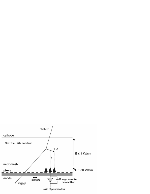
A pixelized micromegas bulk [9] is used in order to perform a 3D reconstruction of a few mm track. It is segmented in 350 µm pixels associated to a dedicated ASIC described here. The pixels of each 96 x-rows are linked in jumps of 1 pixel over the 96 y-columns ones forming an interwoven anode of strips of pixels. Indeed, for a given x-row, one out of two pixels is connected to the same strip. Then, for the next x-row, pixels are connected in a staggered arrangement. Same rule apply for y-columns. The location of the pixels fired is then obtained by using the coincidence among the x and y strips. This read-out strategy permits to reduce the number of channels for covering a large anode surface as needed for the direct dark matter detection. As shown on figure 1, the coordinates in the anode plane (x and y coordinates) are reconstructed by collecting primary electrons produced in the drift region with an electric field (1 kV/cm) and amplified in the avalanche region (80 kV/cm). The recoil is thus projected on the anode, providing 2D information on the track. As stated above, 3D track reconstruction is needed for directional detection of dark matter. This is achieved by sampling the anode signal every 25 ns. Knowing the electron drift velocity, information on the third coordinate is retrieved. For instance, in at 350 mbar with a drift field of 200 V/cm, the drift velocity is 16 µm/ns and the recoil track is then decomposed in voxels of typically µ. A dedicated 3D reconstruction algorithm has been developed, allowing to reach an angular resolution better than . More details may be found in [10].
2 Design of the front end ASIC
2.1 Background
The MIMAC detector is planned to be a multi-target detector, i.e. composed of a matrix of chambers filled with several gases. In order to define the ASIC specifications, we focused on 3He and 19F. In the case of 3He the following informations have been used:
-
1.
the mean energy to produce a e- / ion pair is 41 eV;
-
2.
the drift velocity is 16 µm/ns at 350 mbar and a drift field of 200 V/cm;
-
3.
chamber gain is 5000;
-
4.
minimum signal is (approximated to a current triangular pulse with a base width of 5 ns and an amplitude of 300 nA );
-
5.
with a drift field of 200 V/cm and a pressure of 350 mbar, the electron cloud radius at one due to the diffusion is roughly 450 µm where L is the distance from the point of interaction to the anode.
Directional detection of dark matter implies the measurement of low energy recoil tracks. Typically, for a 3He µTPC detector, the range of interest for dark matter lies below 10 keV (50 keV for ), with a sub-keV threshold. Moreover, this µTPC detector will be used for neutron metrology up to higher energies (2 MeV) [11]. Hence, the prototype ASIC has been designed and developed with extra functionalities to demonstrate that the gaseous chamber associated with its electronics can measure the energy and track of particles over a wide range of energies. This will allow the measurement of low energy electrons (used for calibration purposes), low energy nuclear recoils (from WIMP interaction) and even MeV alpha particles. This implies a track measurement with lengths ranging from a few millimetres to a few centimetres. Table 1 presents ranges and energy losses for various particles. For the ASIC specification, a dynamic range from 300 eV to 1000 keV was chosen. It should be noticed that even for an incoming alpha particle at high pressure the energy channel could saturate and in that case the track length would be enough for discrimination.
| Range | Energy | |
| (pressure and gas dependant) | ||
| X-source 55Fe: e- | 6 mm (1 bar) to | 5.9 keV |
| 18 mm (350 mbar) | ||
| source 57Co: | 1 mm 1 cm | 0.5 keV; 5 keV |
| internal conversion e- | (1 bar) | 7 keV; 13 keV |
| ion source: | few µm to few mm | from 0.5 50 keV |
| 3He and 4He recoils | ||
| neutron capture | 5 cm (p+) (1 bar) | 100 keV/cm |
| 573 keV + 191 keV | ||
| Alpha | up to chamber size (350 mbar) | 5 MeV |
The lowest charge that has to be measured by ionization in the dynamic range chosen is 300 eV equivalent to 1 keV recoil at 350 mbar [12]. It will produce, in the case of , 7-8 primary electrons that will drift to the amplification space covering a surface determined by the square root of the drift distance in cm. Therefore, the lowest charge to measure will be defined by the gain ( 5000) which has to permit the detection of a primary electron giving 5000 e- on one strip of pixels. Knowing the approximate shape of the signal, the lowest current to measure is 300 nA. This narrows the choice of the front end amplification electronics to a charge preamplifier (no current leakage and low noise).
2.2 Architecture overview
The front end chip is composed of sixteen channels as presented on figure 2. Each channel consists of a charge preamplifier with two outputs. Its voltage output is connected to one of the sixteen inputs of a common summing shaper and its current output feeds a discriminator. The sixteen discriminator outputs are sampled and serialized over two differential lines in order to reduce the system connections. The summing shaper provides the energy released in the detector with two gains. Low gain range is from 300 eV (noise level) to 1 MeV and high gain range is from 300 eV to 80 keV. The position and the inclination of the incident particle track are provided in real time by the digital outputs via the signal duration.

2.3 Input stage
In order to maximize the signal to noise ratio, the input stage (see figure 3) consists of a low noise charge preamplifier based on a folded cascode structure with a large interdigitated PMOS input transistor [5000 µm/0.35 µm]. Due to the fact that the electronics are auto triggered the capacitor is discharged through a resistor with a decay time constant of 8 µs. To obtain the total energy signal, the voltage output is connected to one of the sixteen shaper inputs to be summed and filtered.

The integration current, flowing through the capacitor, is copied and amplified with a gain of 15 to generate the input signal of the current comparator [13].
Two cascode transistors were added to the CMOS inverter, here used as an amplifier, in order to decrease the influence of the input to output parasitic capacitor. Optimal vn2 and vp2 values were determined by simulation. Also, for improving the comparator commutation speed, the CMOS inverter is kept in linear mode by the use of the two feedback transistors. The other benefit of this architecture is that the injected charges in the transistors grids is minimized, therefore further decreasing the turn on and turn off times. Vn1 and vp1 are adjusted by simulation for barely maintaining the two feedback transistors “OFF” in the quiescent state of the comparator (no input current, no threshold applied). When a threshold current (provided by a 5 bit DAC) is applied, one of the two feedback transistors starts conducting allowing the current flow. Then, when an input current higher than the current threshold is applied, the previously conducting transistor is switched off, the CMOS inverter toggles and the other feedback transistor starts conducting. At the output, the comparator delivers a digital signal whose duration is equal to the current duration. This signal is sampled at a rate of 40 MHz. Biasing voltages “vnx” and “vpx” are internally generated.
In order to be able to use this reduced resolution DAC, a trade off has been made and an auto zero amplifier has been added for minimizing the DC offset current in the output branch of the preamplifier (essentially due to transistor mismatches) and thus optimizing the usable DAC range.
At a slow rate (1 Hz) the current output of the preamplifier is disconnected from the discriminator and connected to one of the differential amplifier inputs.
The offset current charges or discharges a capacitor and the amplifier compares the voltage capacitor to the DC input voltage of the current comparator.
The offset correction is applied to the output branch via a current mirror and the “control” line. During the auto-zero DC correction, a certain isolation to the input signal has to be implemented in order to provide adequate offset cancellation. For this, series resistors and long channel transistors have been added. The gate voltage “V_clamp”, which is accessible outside of the ASIC, provides an adjustment of the filtering time constant.
2.4 Energy channel
To measure the total energy released in the ionisation channel by the incident particle, the sixteen preamplifier outputs are summed and filtered. The signal duration depends on the track inclination, it can last from 10 ns (track of 300 µm in 3He at 1 bar) up to 6 µs (track of 15 cm). A CR-RC3 structure has been chosen for the shaper with two gains in a ratio of 12.5 and a time constant of 200 ns (figure 4). The higher gain increases the precision of the energy measurement in the lower range (up to 80 keV) corresponding to most of the expected experimental results. For the time constants the passive components are realized with specific layers available in the SiGe process: high resistivity polysilicon and polysilicon-sinker (bipolar collector) for the capacitor.

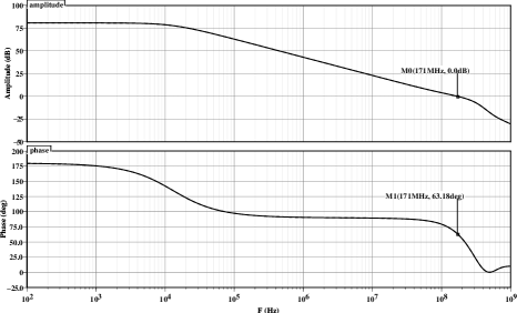
All the operational amplifiers are based on a similar structure (figure 5) to achieve a gain bandwidth of 170 MHz with a phase margin of 63∘ and an open loop gain of 80 dB fully compatible with the gains and time constants chosen for the shaper (figure 6).

The oscillogram (see figure 7) shows the response of the charge preamplifier and the high gain shaper to an input current pulse.
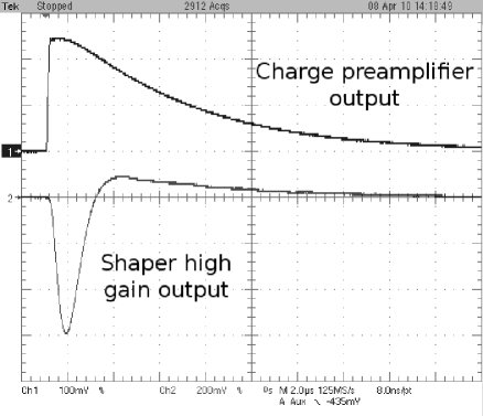
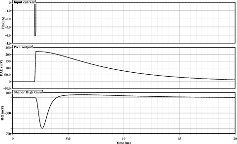
They are in good agreement (with respect to amplitude and peaking time) with the simulation results (figure 8). It can be noted that the preamplifier non-exponential decay is due to the parasitic capacitance of the 4 M feedback resistor (figure 3), implemented in the high resistivity polysilicon layer, and that it has no negative impact on the shaper output.
2.5 Serializer
One major difficulty of this front end ASIC is to get all the comparator outputs out of the chip. This is a concern for several reasons. First, the interconnection has to be kept to a minimum in order to equip large detectors and second, the noise level induced by these outputs has to be kept low. This last reason leads to the choice of LVDS differential output. The problem is that this kind of standard display other difficulties, large number of outputs (two times the number of inputs; one has to remember that the complete MIMAC detector will have around 1000 channels), large current consumption and thus large power dissipation. The remedy to this is to implement a serializer that will work 8 times faster and thus time multiplex data into a single differential pair.
Instead of providing the 8 differential data at a rate of 40 MHz, the data can be transferred on a single pair at a rate of 320 MHz. Using this solution, one more signal (differential as well) is required for synchronization, it is the 40 MHz reference clock, it avoids to carry an extra signal commutating at 320 MHz. When taking a close look at the waveform (see figure 9), one can see that each bit is always at the same time offset from the reference clock rising edge. This synchronisation signal can be shared by a large number of serializer outputs, as long as each serializer uses the same 320 MHz clock.

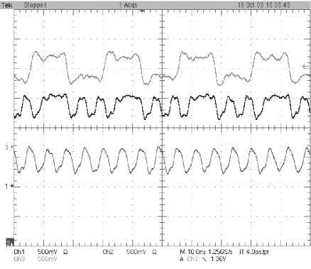
The 320 MHz clock is generated by a Phase Locked Loop circuit synchronized with the 40 MHz reference clock. This “classical” PLL structure [14] needs only passive external components for the charge pump reference current and filter. The LVDS transmitter and receiver are based on structures described in [15]. For testing purposes, a multiplexer is implemented just before the serializer. That enables the user to select either the sending of a known pattern or the comparator output. The oscillogram of the outputs can be seen in figure 10, where a fixed pattern was sent, bottom is serial data 0xAA, middle is the serial data 0xEA, top is the input clock of 40 MHz.
3 Validation of the front end ASIC with the prototype detector
In order to validate the front end ASIC design and concept, a prototype anode featuring strips of pixels was coupled to an acquisition board. It was equipped with ASICs and FPGAs for triggering and hardware level processing. Each strip composed of 96 pixels was connected to one ASIC input channel. The digital outputs were connected directly to the FPGA and the shaper outputs were used to feed peak detectors coupled with ADCs. The FPGA uses the de-serialized front end digital output information for local triggering (an OR of the 16 discriminator outputs). There are as many local triggers and pre processors as ASICs. For each trigger, the FPGA records and decodes each ASIC track informations (pre-processing stage) and retrieves the shaper amplitude from the relevant ADC.
In the last stage of the hardware processing, the track and energy informations issued by the ASIC monitoring the involved pixel strips are merged and transferred to the reconstruction and on-line display software.
4 Conclusion
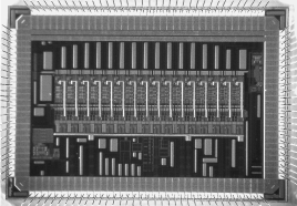
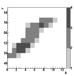
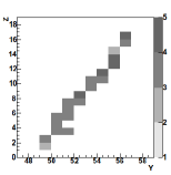
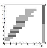
Twelve of these prototype chips (figure 11) have been mounted on a prototype µTPC composed of strips of pixels covering . The detector has been used in various experimental configurations. The data acquisition electronics board and software will be presented in a forthcoming paper [16]. A dedicated 3D reconstruction algorithm is needed to take full advantage of the potential of the detector [10]. As an example, a 3D track reconstruction obtained with a MIMAC prototype detector is presented in figure 12. It has been obtained in 95% at a pressure of 350 mbar and with a drift field of 200 V/cm. Figure 12 presents this track projected on the X,Y plane (the anode one) on the left panel. The middle (resp. right) panel presents the track measurement in the Y,Z (and X,Z) plane. This example outlines the possibility to obtain 3D track measurement down to keV energy particles with a gaseous µTPC equipped with the front end ASIC presented in this paper.
It has been shown by simulations and experimental results, that the MIMAC ASIC offers great possibilities for 3D track reconstruction and ultimately for
directional dark matter detection.
A 64 channels version of this ASIC is under test, it includes some minor improvements such as:
-
1.
Increased shaper time constant in order to reduce the energy measurement difference between short and long duration tracks
-
2.
An increase of the maximum serial rate in order to reach the 50 MHz sampling rate
-
3.
Removal of the synchronisation clock (known patterns will be used for synchronisation)
-
4.
The addition of a stretcher after each discriminator in order to cope with short duration tracks ( 20 ns)
Acknowledgement
C.G and the MIMAC collaboration acknowledge the ANR-07-BLAN-0255-03 funding.
References
- [1] D. N. Spergel, Phys. Rev. D 37 (1988) 1353
- [2] J. Billard et al., arXiv0911.4086
- [3] A. M. Green and B. Morgan, Astropart. Phys. 27 (2007) 142
- [4] S. Ahlen et al., International Journal of Modern Physics A25 (2010) 1-51, arXiv:0911.0323
- [5] C. Grignon et al., JINST 4 (2009) P11003, arXiv:0909.0654v3
- [6] F. Mayet et al., J. Phys. Conf. Ser. 179 (2009) 012011
- [7] D. Santos et al., J. Phys. Conf. Ser. 65 (2007) 012012
- [8] Y. Giomataris et al., Nucl. Instr. and Meth. A376 (1996) 29
- [9] Y. Giomataris et al., Nucl. Instr. and Meth. A560 (2006) 405
- [10] C. Grignon et al., 3D Track reconstruction for directional dark matter detectors, in preparation.
- [11] A. Allaoua et al., Radiat. Meas. 44 (2009) 755, arXiv:0812.0336
- [12] D.Santos et al., arXiv:0810.1137
- [13] G. Linan-Cembrano, R. Del Rio-Fernandez, R. Dominguez-Castro, A. Rodriguez-Vasquez, Electronics Letter volume 33, issue 25 (1997) p2082-p2084
- [14] D. Dzahini, J. Pouxe, O. Rossetto, IEEE TNS 47 (2000) 3 (839-843)
- [15] A. Boni, A. Pierazzi, D. Vecchi, IEEE J. of Solid State Circuits. 36 (2001) 4 (706-711)
- [16] O. Bourrion et al., Data acquisition electronics and reconstruction software development for Dark Matter directional detection with MIMAC, in preparation