Nonlocal transport in the charge density waves of -TaS3
Abstract
We studied the nonlocal transport of a quasi-one dimensional conductor -TaS3. Electric transport phenomena in charge density waves include the thermally-excited quasiparticles, and collective motion of charge density waves (CDW). In spite of its long-range correlation, the collective motion of a CDW does not extend far beyond the electrodes, where phase slippage breaks the correlation. We found that nonlocal voltages appeared in the CDW of -TaS3, both below and above the threshold field for CDW sliding. The temperature dependence of the nonlocal voltage suggests that the observed nonlocal voltage originates from the CDW even below the threshold field. Moreover, our observation of nonlocal voltages in both the pinned and sliding states reveals the existence of a carrier with long-range correlation, in addition to sliding CDWs and thermally-excited quasiparticles.
pacs:
71.45.Lr, 72.15.NjNonlocal properties in charge density waves (CDW) have been attracting interest for decades Gill1982 ; Ramakrishna1992 ; Lemay1996 . Since electric transport phenomena include collective motion Gruner , it is natural to expect a sliding CDW to be a possible source of nonlocal transport Gill1982 . The correlation of the CDW phase has been estimated in the 1 to 100 m range Gill1982 ; Mihaly1983 ; Thorne1985 ; Lyding1986 ; Borodin1987 ; Sweetland1990 ; McCarten1992 ; Danneau2002 ; LeBolloch2008 ; Tsubota2009 , which is long enough to allow experimental studies. The correlation inside the sliding region has been confirmed. However, it has been shown that the correlation of a sliding CDW does not extend far beyond the electrodes, where phase slippage may destroy the correlation Ramakrishna1992 ; Lemay1996 .
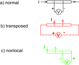
In this article, we report a nonlocal transport phenomenon with a quasi-one dimensional conductor -TaS3. Following the pioneering work by Gill Gill1982 , we compared current-voltage characteristics obtained with normal and transposed electrode configurations, as well as with nonlocal detection (Fig. 1). We found that nonlocal voltages appeared in the CDW of -TaS3, both below and above the threshold field for CDW sliding. The sign of the observed nonlocal voltage was opposite to that of the spreading resistance Borodin1986 ; Slot2001 . In addition to this, the temperature dependence of the nonlocal voltage suggests that the observed nonlocal voltage originates from the CDW. Moreover, our observation of nonlocal voltages in both the pinned and sliding states reveals the existence of a carrier with long-range correlation, in addition to sliding CDWs and thermally-excited quasiparticles. Finally, we compared our observation to the coexistence of two CDWs in -TaS3 Inagaki2008 ; Toda2009 , and found it is closely related to topological dislocations in CDWs.
We performed a four-probe measurement, which requires a voltmeter with a high input impedance so that the leakage current to the voltmeter becomes negligible. For fully-gapped CDW materials, such as -TaS3, the use of four-probe measurement is usually difficult especially at low temperatures where the sample resistance often exceeds the typical input impedance of a voltmeter, for example, G. We exploited an electrometer (Keithley 6512, T) to measure the voltage drop of the -TaS3 samples.
-TaS3 crystals were synthesized with a standard chemical vapor transport method. A pure tantalum sheet and sulfur powder were put in a quartz tube. The quartz tube was evacuated to Torr and heated in a furnace at 530 ∘C for two weeks. The electrodes were made using 50-m-diameter silver wires glued with silver paint. Gold thin film was deposited on the crystal before the silver wires were attached to reduce the contact resistance to 1 at room temperature. The spacing between the electrodes was typically 200 m, and the sample cross section was m2 (width thickness).
Figure 2 shows the temperature dependence of the resistance of a -TaS3 crystal. The result shows the well-known features of -TaS3, a Peierls transition temperature of 220 K, an Arrhenius-type temperature dependence with an activation energy of 790 K, and a deviation from the Arrhenius plot below 100 K. We checked the contact resistance by comparing the four- and two-terminal resistances, and found it was negligible in the room temperature to 40 K range. We also confirmed that the result was unaffected by the difference between substrates by comparing data obtained with the silica and sapphire substrates. Based on these considerations, we confirmed that the four-terminal measurement was properly performed over the entire temperature range of the measurement.
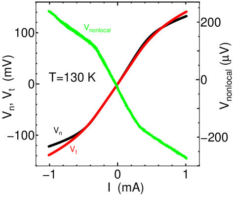
Figure 3 shows the current-voltage (-) characteristics at 130 K in the normal and transport configurations, as well as the nonlocal voltage. The - characteristics with the normal configuration (black line) and with the transposed configuration (red line) coincide in a low current regime where ohmic behavior is observed. Above the threshold of nonlinear conduction, we detected a discrepancy between the two configurations. This discrepancy can be understood as the phase-slip voltage accompanied by CDW sliding Gill1982 ; Ramakrishna1992 . When the CDW slides under a condition where the regions outside the current electrodes are strongly pinned, elastic deformation is induced in the CDW. In the vicinity of each electrode, the elastic deformation relaxes by breaking CDW phase continuity. In the transposed configuration (Fig. 1 b), the measured voltage is affected by the phase slip, in contrast to the normal configuration (Fig. 1 a), hence the difference between these two configurations as shown in Fig. 3 reveals that the phase slip really occurred in the sample.
We also observed nonlocal voltage as shown in Fig. 3 (green line), by using the nonlocal configuration (Fig. 1 c). The result shows that at 130 K, a negative voltage was detected at a pair of electrodes 200 m away. The magnitude of the nonlocal voltage was around 200 V at 1 mA. This voltage was large enough to be measured with our ultra-high impedance voltmeter, whose minimum detectable voltage was 10 V. The voltage was proportional to the injected current, with kinks at mA, above which the slope of the - curve became moderate. The emergence of a voltage at the nonlocal probes is fascinating since Gill reported that there was no detectable signal in the CDW state of NbSe3 Gill1982 . Such an attempt has also been made for other CDW systems, however, the nonlocal effects were unlikely to extend over the electrode, except via strain distribution Lemay1996 .
We first compared our observation with a trivial source, known as spreading resistance, which could affect the nonlocal voltage probes Borodin1986 ; Slot2001 . When the current is injected from a tiny electrode into a bulk sample, it cannot flow homogeneously until it spreads over a cross section. In the vicinity of the electrodes the flow lines are curved, and some of them travel in the opposite direction to the counterelectrode. At the sample surface the electric potential of position is expressed by
| (1) |
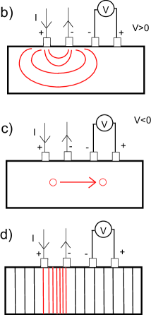
where denotes an applied field, is the electrode length, and is a reduced thickness with being the anisotropic ratio of conductivity Borodin1986 ; Slot2001 . In addition, the effective cross section for the current is limited to the specific distance , and an additional contribution to resistance emerges, known as spreading resistance. An important feature of spreading resistance is that it obeys Ohm’s law since its nature is the restriction of the current path. In our configuration for nonlocal detection (Fig. 1 c), the contribution of the spreading resistance must generate a positive voltage between the voltage probes.
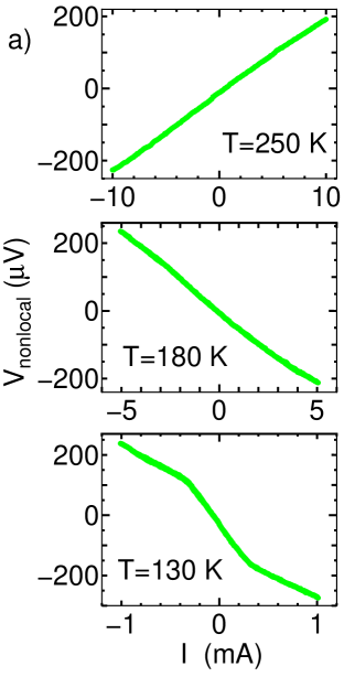
In fact, the observed nonlocal voltages were negative as shown in Fig. 3. Moreover, the temperature dependence of the nonlocal voltage suggests that CDW is closely related to its origin. Figure 4a shows the temperature evolution of the nonlocal voltages at 130, 180, and 250 K. At 180 K, although the kink and nonlinearity became less pronounced, the nonlocal voltage was negative. In contrast, at 250 K, above the Peierls transition ( K), the polarity was reversed, and became positive. The slope of the - curve was . This is in good agreement with the estimation of spreading resistance estimated using Eq. (1) with an anistropy ratio of Slot2001 . To confirm this is not an artifact from the measurement circuit, we performed several sets of experiments, including a comparison of the data while inverting the polarity of the electrodes of both the current generator and the voltmeter. We also checked the reproducibility by using different specimens and cryostats. All the data were consistent and we concluded that the observed negative nonlocal voltage was really a property of the samples. Hence it is unlikely that the nonlocal voltage can be attributed to the trivial spreading resistance, whereas its attribution to CDW is plausible.
In addition, the voltages were nonlinear functions of the current with apparent kinks (Fig. 3). The positions of the kinks in the nonlocal voltage were found to be close to the threshold of nonlinear conduction of the CDW. When the sample was in a CDW state the Peierls gap opens at Fermi surfaces, so that thermally-activated quasiparticles and collective motion of the CDW contribute to electric conduction. The former provides ohmic currents, and as discussed above, might contribute to positive nonlocal voltages. Hence, a quasiparticle is also ruled out as a major contributor to the nonlocal voltage, and the collective motion becomes a candidate for the nonlocal voltage. Nevertheless, the observed kinks are clearly related to the onset of CDW sliding.
For the sliding CDW to provide the nonlocal voltage, probed 200 m away from the emitting electrodes, the phase correlation length of the CDW should be at least comparable to or longer than the travelling length. There are several estimations for the phase correlation length, ranging from 1 to 100 m Gill1982 ; Mihaly1983 ; Thorne1985 ; Lyding1986 ; Borodin1987 ; Sweetland1990 ; McCarten1992 ; Danneau2002 ; LeBolloch2008 ; Tsubota2009 . X-ray diffraction typically provides the lengths of the order of 1 m Sweetland1990 ; Danneau2002 ; LeBolloch2008 , whereas other kinds of estimations based on CDW dynamics provide longer values of up to 100 m Gill1982 ; Thorne1985 ; Lyding1986 ; Tsubota2009 . Moreover, the phase coherence length is a strong function of defect concentration, and will differ for different materials and even for samples of the same material. Consequently, a consideration of the correlation length does not deny the possibility of a sliding CDW being the origin of the nonlocal voltage.
However, even if the CDW correlation could extend such a distance, the standard interpretation of the phase-slip voltage suggests that the phase correlation might be lost in the vicinity of the electrode Gill1982 ; Ramakrishna1992 . As shown in Fig. 3, the difference between the voltages of the normal and transposed configurations implies that the CDW is in the sliding state with a considerable rate of phase slip Ramakrishna1992 . Moreover, it should be noted that the nonlocal voltage was observed even below the kinks. Hence, the source of the nonlocal voltage must be present whether or not the CDW slides.
Now we may propose a possible model based on the above discussions. Since the CDW phase correlation is destroyed in the vicinity of the electrodes, and the nonlocal voltage is also seen below the kinks, we must seek for a different transport mechanism originated from the CDW state, rather than sliding. Its properties should include ohmic behavior, and it should possess a spatial correlation over at least 200 m. A recent synchrotron diffraction study reports that two kinds of CDWs, incommensurate and commensurate CDWs, coexist in -TaS3 Inagaki2008 , and a subsequent ultrafast optical pump-probe study of -TaS3 also provides evidence for two types of CDW phases Toda2009 . Discommensuration, or a lattice of topological dislocations McMillan1976 exists from the Peierls temperature to around 50 K Inagaki2008 . Each topological dislocation is accompanied by a charge, which can move along the chain direction of a CDW. The distance between dislocations is determined by the difference between the CDW wavelength and the lattice constant of the pristine lattice. The advantage of this model as regards explaining the nonlocal voltage relies on the correlation length of the dislocation lattice. Hence the question now moves to how far can the correlation be extended.
Coulomb repulsion plays a major role in the interaction between the dislocations since each dislocation is accompanied by an electric charge. In some CDW materials, such as NbSe3, uncondensed electrons remain at the Fermi surface, leading to the screening of the Coulomb potential. In the case of -TaS3, the entire Fermi surface contributes to the CDW, and at low temperatures the density of thermally-activated quasiparticles is very low, so that the screening of the Coulomb potential becomes negligible. This helps to increase the correlation length of the dislocation lattice. We believe this is the most plausible model for explaining the observed nonlocal voltage.
Consequently, the observed nonlocal voltage may have three difference origins, as expressed by
| (2) |
where , , and denote spreading resistance, the correlated motion of the dislocation lattice, and CDW sliding, respectively. Under our experimental conditions, each term contributes as follows: for all temperatures; and below the Peierls temperature; and above the CDW sliding threshold. Each term is schematically illustrated in Figs. 4b-4d. By using these terms, Eq. (2) provides qualitative explanations for the observed peculiar behavior as shown in Figs. 3 and 4. It should be noted that the polarity of is positive, thus coinciding with . This might be caused by the backflow of quasiparticle current accompanied by CDW sliding vdZ2001 .
Finally, we discuss the possible relationship between our observation and the soliton transport in a commensurate CDW Gruner . Previous studies have suggested that the low temperature transport of -TaS3 should be understood as a CDW soliton Maki1977 ; Takoshima1980 . Experimentally, the anisotropy of conductivity was found to be increased at low temperatures along the chain direction Takoshima1980 . Although the excitation energy was estimated to be 250 K, the previous results failed to detect any traces of the soliton at temperatures at which they should be excited. Assume that our observation of nonlocal voltage is an emergence of soliton transport. The phase diagram of -TaS3 Inagaki2008 shows that there is commensurate CDW at 130 K. Hence, if the life time of the excited soliton is long enough to travel over the 200 m, it can be a candidate to the origin of the nonlocal voltage. Since we lack unambiguous evidence for the relationship to the CDW soliton within our study, we will pursue the nature of this nonlocal voltage in further studies, including the use of optical Toda2009 , acoustic Malomed1993 and diffraction Inagaki2008 ; LeBolloch2008 methods.
To summarize, we studied the nonlocal transport of a quasi-one dimensional conductor -TaS3. We found that nonlocal voltages appeared in the CDW of -TaS3, both below and above the threshold field of CDW sliding. The temperature evolution of the nonlocal voltage suggests that the observed nonlocal voltage originates from the CDW. Moreover, our observation of nonlocal voltage in both the pinned and sliding states reveals the existence of a carrier with long-range correlation, in addition to a sliding CDW and thermally-excited quasiparticles.
We are grateful to K. Ichimura, K. Yamaya, Y. Toda, M. Hayashi and Y. Nogami for fruitful discussions. One of the authors (K.I.) thanks the Japan Society for the Promotion of Science for financial support via a Grand-in-aid for Scientific Research (Kakenhi).
References
- (1) J. C. Gill, Solid State Commun. 44, 1041 (1982).
- (2) S. Ramakrishna, M. P. Maher, V. Ambegaokar, and U. Eckern, Phys. Rev. Lett. 68, 2066 (1992).
- (3) S. G. Lemay, R. E. Thorne, M. C. Saint-Lager, and P. Monceau, Phys. Rev. B 54, 16341 (1996).
- (4) G. Grüner, Density Waves in Solids, Addison-Wesley, Reading (1994).
- (5) G. Mihály, Gy. Hutiray, and L. Mihály, Phys. Rev. B 28, 4896 (1983).
- (6) R. E. Thorne, J. H. Miller, Jr., W. G. Lyons, J. W. Lyding, and J. R. Tucker, Phys. Rev. Lett. 55, 1006 (1985).
- (7) J. W. Lyding, J. S. Hubacek, G. Gammie, and R. E. Thorne, Phys. Rev. B 33, 4341 (1986).
- (8) D. V. Borodin, S. V. Zaĭtsev-Zotov, and F. Ya. Nad’, Sov. Phys. LETP 66, 793 (1987).
- (9) E. Sweetland, C-Y. Tsai, B. A. Wintner, J. D. Brock, and R. E. Thorne, Phys. Rev. Lett. 65, 3165 (1990).
- (10) J. McCarten, D. A. DiCarlo, M. P. Maher, T. L. Adelman, and R. E. Thorne, Phys. Rev. B 46, 4456 (1992).
- (11) R. Danneau, A. Ayari, D. Rideau, H. Requardt, J. E. Lorenzo, L. Ortega, P. Monceau, R. Currat, and G. Grübel, Phys. Rev. Lett. 89, 106404 (2002).
- (12) D. Le Bolloc’h, V. L. R. Jacques, N. Kirova, J. Dumas, S. Ravy, J. Marcus, and F. Livet, Phys. Rev. Lett. 100, 096403 (2008).
- (13) M. Tsubota, K. Inagaki, and S. Tanda, Physica B: Condensed Matter, 404, 416 (2009); arXiv:0906.5206.
- (14) D. V. Borodin, S. V. Zaĭtsev-Zotov, and F. Ya. Nad’, Sov. Phys. LETP 63, 184 (1986).
- (15) E. Slot, H. S. J. van der Zant, and R. E. Thorne, Phys. Rev. B 65, 033403 (2001).
- (16) K. Inagaki, M. Tsubota, K. Ichimura, S. Tanda, K. Yamamoto, N. Hanasaki, Y. Nogami, N. Ikeda, T. Ito, and H. Toyokawa, J. Phys. Soc. Jpn. 77, 093708 (2008).
- (17) Y. Toda, R. Onozaki, M. Tsubota, K. Inagaki, and S. Tanda, Phys. Rev. B 80, 121103(R) (2009).
- (18) W. L. McMillan, Phys. Rev. B 14 1496 (1976).
- (19) H. S. J. van der Zant, E. Slot, S. V. Zaitsev-Zotov, and S. N. Artemenko, Phys. Rev. Lett. 87, 126401 (2001).
- (20) T. Takoshima, M. Ido, K. Tsutsumi, T. Sambongi, S. Honma, K. Yamaya, and Y. Abe, Solid State Commun. 35, 991 (1980).
- (21) K. Maki, Phys. Rev. Lett. 39, 46 (1977).
- (22) B. A. Malomed, J. Phys. Soc. Jpn, 62, 997 (1993).