Complex evolution of the electronic structure from polycrystalline to monocrystalline graphene: generation of a new Dirac point
Abstract
First calculations, employed to address the properties of polycrystalline graphene, indicate that the electronic structure of tilt grain boundaries in this system display a rather complex evolution towards graphene bulk, as the tilt angle decreases, with the generation of a new Dirac point at the Fermi level, and an anisotropic Dirac cone of low energy excitations. Moreover, the usual Dirac point at the K point falls below the Fermi level, and rises towards it as the tilt angle decreases. Further, our calculations indicate that the grain-boundary formation energy behaves non-monotonically with the tilt angle, due to a change in the the spatial distribution and relative contributions of the bond-stretching and bond-bending deformations associated with the formation of the defect.
pacs:
73.22.-f,68.65.-kGraphene - an isolated layer of -bonded carbon atoms arranged in a honeycomb structure - was until very recently, a “theoretical” reference system for the study of the properties or the “real” -bonded carbon forms, such as fullerenes, nanotubes, and graphite rmp ; novos07 ; nakada ; wallace . Since the recent report of the isolation of a stable single-atom-thick carbon layer, by exfoliation of graphite novos04 , graphene itself has occupied the center stage of Materials Physics, as a paradigmatic system for “relativistic” condensed-matter phenomena, as well as a promising material for Nanoelectronics, due to its exceptional electronic properties. Graphene is a null-gap semiconductor with a vanishing density of states at the Fermi level, and electronic bands that are linear and isotropic within 1 eV from the Fermi level. This linearity and the presence of two sub-lattices imply that charge carriers in graphene effectively behave as massless chiral “relativistic” particles, being described by Dirac’s equation. rmp ; novos07 ; wallace Due to the chiral nature of the electronic excitations, which leads to the absence of backscattering, graphene holds ballistic charge transport on the microscale, even at room temperature, and with high concentrations of defects and impurities. rmp ; novos07 ; novos04 ; kats06 In the last few years, scientific interest in graphene has rapidly intensified, and the material is expected to play a major role in Nanoelectronics in the future.
Presently, common synthesis routes for graphene are the original exfoliation method, novos04 that produces monocrystalline graphene samples, and epitaxy, mostly on SiC deheer and metallic substrates sinitsyna . Recent works on epitaxially-grown graphene report the occurrence of superstructures interpreted as Moiré patterns laura ; datta based on STM, AFM, and STS measurements. Moiré patterns and superstructures, associated with layer stacking, as well as the occurrence of bulk and surface grain boundaries, are topics of prominence in the physics of highly-oriented pyrolytic graphite (HOPG) itself. simonis ; gan ; pong ; varchon ; cervenka Grain boundaries (GB) are among the most commonly occurring extended defects in HOPG, because of its polycrystalline character cervenka . For large scale graphene production and application, it is expected that synthesis methods will be epitaxy based, being quite conceivable that polycrystalline samples will be produced. Indeed, the occurrence of GBs on the graphene layer has been recently reported, laura speculated as a probable source of long-range electronic perturbations in graphene on SiO2, datta and further, the lower carrier mobility of epitaxial graphene (when compared with exfoliated samples), in a macroscopic-size graphene field-effect transistor, has been tentatively assigned to the electronic perturbations associated with GBs. gong
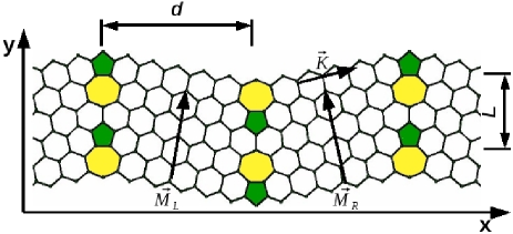
Previous works have addressed the electronic properties of disordered graphene, but these have focused on the effects of point defects, corrugation, and extended edge states in graphene ribbons, drawing only speculative conclusions in what regards the electronic states of GBs. rmp In this scenario, addressing properties of GBs in graphene is of primary relevance. In the present work, we employ first principles calculations to examine the energetics and electronic properties of GBs in graphene. We focus on the structural GB model proposed by Simonis et al., simonis who observed a large-angle tilt boundary on the surface of HOPG, on STM experiments. These authors proposed that, in the absence of stress, the observed GB consists of a periodic structure that can be described as a regular succession of pentagon-heptagon pairs, as shown in Fig. 1. Based on this model, we investigate three GBs of different periodicities along the boundary, hence with different relative orientation between the grains.
We find that, while large-angle tilt GBs do not introduce localized states at the Fermi level in graphene, various resonance peaks appear in the density of states of the material, over a broad energy range, starting at energies of 0.3 eV from the Fermi level, in agreement with recent experimental work. cervenka More importantly, the changes in electronic structure with the GB tilt angle indicate a non-trivial evolution towards graphene bulk, as the GB angle decreases: we observe the generation of a new Dirac point at the Fermi level, which lies on a line that evolves towards the -M direction of the graphene Brillouin zone (BZ), with the usual Dirac point at the K point falling below the Fermi level, and rising towards it as the tilt angle decreases. The Dirac cone of low-energy excitations around this new Dirac point is non-isotropic, with the effective “speed-of-light” depending on the direction in the BZ away from the Dirac point. Furthermore, our calculations indicate that, within the structural model we consider, the GB formation energy does not behave monotonically with the period of the GB (or, equivalently, with the tilt angle). A Keating analysis of the elastic energy, associated with the formation of the defect, indicates that a change in the the spatial distribution and relative contributions of the stretching and bending deformations leads to the non-monotonicity indicated by our results.
. GB1 72 6.6 0.33 0.42 0.10 0.32 GB2 120 10.9 0.42 0.47 0.15 0.31 GB3 168 15.2 0.40 0.41 0.15 0.27
All calculations are performed using Kohn-Sham density functional theory Kohn , the generalized-gradient approximation (GGA) Kleinman for the exchange-correlation term, and norm-conserving Troullier-Martins pseudopotentials Troullier , to describe the electron-ion interaction. We use the LCAO method implemented in the SIESTA code Siesta , with a double-zeta pseudo-atomic basis set plus polarization orbitals, with an energy cutoff of 0.01 Ry. Structural optimization is performed until the total force on each atom is less than 0.02 eV/Å. In order to simulate an isolated honeycomb sheet, we use supercells that are periodic along the graphene plane, and are surrounded by a 33 Å vacuum region, such that the interactions between each layer and its periodic images are negligible.
Periodicity along the graphene plane requires the supercell to contain two GBs of opposite tilt angles (a GB and the corresponding “anti-GB”), as shown in Fig. 1 for the GB1 geometry. The experimental value in Ref. simonis for the relative orientation between grains is , defined here by the angle between vectors and , drawn respectively on the left and right grains adjacent to the GB, as shown in Fig. 1. This model can be extended to GBs with smaller tilt angles, by adding lines of hexagons, such that the period of the pentagon-heptagon pattern along the GB increases. In the () limit, we recover the perfect single-crystal graphene lattice. We study three different GB geometries, with the theoretical values for and indicated in Table 1. GB1 is the model proposed in Ref. simonis , with and Å; GB2 has and Å; and for GB3 and Å. In order to ensure that we simulate the properties of an isolated GB, we consider supercells with increasing distances between the GBs and their periodic images. Formation energy results are converged for Å. The geometric parameters , , and are shown in Fig.1, with values for and given in Table 1.
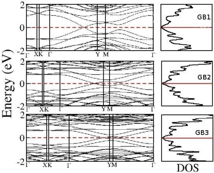
The band-structure of the GB1 (), is shown in Fig. 2(a). The Brillouin zone for this GB supercell is shown in Fig. 3(b). The Y direction is along the GB, and the X direction is perpendicular to it. In Fig. 3(b), we also indicate lines we denoted as M and K, which correspond to these high-symmetry directions in a single-crystal graphene sheet with the orientation of the grain on the right side of the GB. M (and Y) and K (and X) converge to the corresponding directions in the limit, where a single-crystal graphene sheet is recovered. A mirror plane, perpendicular to the graphene sheet and through the geometric center of the GB, relates the M and K lines of the two adjacent grains. Note that the Fermi level or Dirac point occurs on the Y line, in the point marked as in Fig. 3(b), and that band crossings, which lie below the Fermi level, occur at the X and K points.
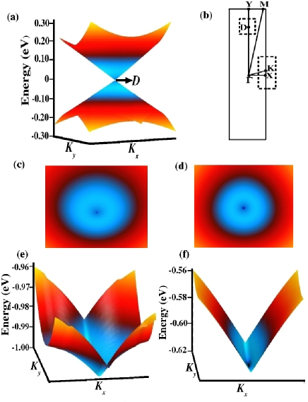
Thus, we observe the generation of a new Dirac cone park , on the Y direction, which is anisotropic, with a Fermi velocity (the effective “velocity of light”) that depends on the direction from the Dirac point in -space. This Dirac cone is shown in Fig. 3(a), for the region around the D point indicated in Fig. 3(b)). The energy isolines are shown Fig. 3(c), where the anisotropy of the cone is clearly displayed: the more (less) elongated is the isoline along a given direction, the smaller (larger) is the Fermi velocity along that direction. The band-structures for the GB2 () and GB3 () are shown in Figs. 2(b) and (c), respectively. Note again the occurrence of a Dirac point at the Fermi level, on the Y line, in both cases. Both display anisotropic Dirac cones as well. The isolines for the GB3, shown in Fig. 3(d), are less anisotropic than in the GB1 case. In Table 2 we include the Fermi velocities for the Dirac cones of the three GBs, along the indicated directions.
The nature of the electronic dispersion in the region around the X and K points, also indicated in Fig. 3(b), are shown in Fig. 3(e) and (f), for the GB1 and GB3, respectively. For the GB3, there is very little dispersion along the X-K direction, resulting in a straight wedge cutting through this line, while in the GB1, the shape of the energy dispersion is also wedge-like, but a “flowery” shape develops at higher energies. Furthermore, the band crossings at the X and K points move up towards the Fermi level, as decreases, which is consistent with the limit, where the Fermi level occurs at the K point. The energy difference between the Dirac point at D and the K point is 1.00 eV for the GB1, 0.73 eV for the GB2, and 0.64 eV for the GB3.
These results indicate a very complex evolution of the band-structure of polycrystalline graphene with the GB angle. Since fivefold and sevenfold topological defects constitute the core of low-energy dislocations in graphene, vozmed they are probably ubiquitous in any realistic model of GBs in this material. Hence, the occurrence of a new Dirac point along the GB direction may prove a robust feature of polycrystalline graphene. We note that previous works have found that, while pentagon-heptagon pairs and the related SW defect introduce no resonant states at the Dirac point in graphene, resonance peaks appear in the density of states starting at a few tenths of an eV from the Fermi level, a result that we have also reproduced with the ab initio method employed here. Our GB electronic structure calculations show, however, that the periodic superstructure formed by these dislocations along the GB line shares with perfect graphene the vanishing gap and the Dirac-like nature of electronic excitations, but in a rather complex structure, with direction-dependent Fermi velocities, the generation of a new Dirac point on the GB direction, and a wedge-like dispersion around the K point that should evolve towards the graphene Dirac cone as . We expect charge transport in polycrystalline graphene to reflect the anisotropic structure of the Dirac cones we obtain in our calculations.
| GB1 | 0.73 | 0.52 | 1.06 | 0.69 | 0.60 | 0.60 |
| GB2 | 0.64 | 0.43 | 0.91 | 0.63 | 0.52 | 0.52 |
| GB3 | 0.55 | 0.45 | 0.53 | 0.55 | 0.57 | 0.57 |
We turn now to the GB energetics. The GB formation energy per unit length is given by , where and are the calculated total energies of the GB and bulk graphene supercells, respectively. The factor of two on the right-hand side accounts for the presence of two GBs in the cell.
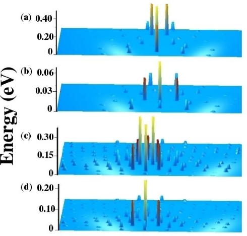
Results in Table 1 show that varies non-monotonically with the GB period. Among the three GBs, GB1 with a tilt angle of has the smallest formation energy, while GB2 with has the highest value. We expect that as . Our results indicate that initially increases, before reaching this asymptotic limit. Given the absence of broken bonds in the GB geometries, is primarily of elastic nature. In order to understand this non-monotonic behavior, we use a Keating model to analyze the bond-bending , and bond-stretching contributions to the GB elastic energy . The results are shown in Table 1. For the GB1 we observe that is a factor of 3.2 larger than , while for the GB2 and GB3 structures the ratio decreases to 2.1 and 1.8 respectively. These results remain essentially unaltered for different choices of the ratio between the stretching and bending energy parameters of the Keating model. Moreover, the spatial distribution of and changes as decreases, as shown in Fig. 4. For the GB1, is largely concentrated on the atoms at the very core of the boundary, mainly in the pentagon-heptagon pairs, while is a little more spread out towards the interior of the grains. For GB3, we see that both and have significant contributions from atoms in the interior of the grain, mostly on the hexagon lines that at the pentagon-heptagon at the boundary. Thus, by concentrating the elastic energy on bending distortions at the defect core, the GB1 structure relaxes to a lower energy state than GBs with smaller angles, which leads to the non-monotonic behavior of .
To conclude, ab initio calculations indicate that the electronic structure of tilt GBs in graphene display a complex evolution towards graphene bulk, as the GB angle decreases, with the generation of a new Dirac point at the Fermi level, lying on a line that evolves towards the -M direction of the graphene Brillouin zone, at the vertex of an anisotropic electronic-energy cone. Moreover, the usual Dirac point at the K point falls below the Fermi level, and rises towards it as the tilt angle decreases. Furthermore, our calculations indicate that the GB formation energy behaves non-monotonically with the tilt angle, due to a change in the the spatial distribution and relative contributions of the bond-stretching and bond-bending deformations associated with the formation of the defect.
Acknowledgements.
We acknowledge support from the Brazilian agencies CNPq, FAPEMIG, Rede de Pesquisa em Nanotubos de Carbono, INCT de Nanomateriais de Carbono, and Instituto do Milênio em Nanotecnologia-MCT.References
- (1) A. H. C. Neto et al., Rev. Mod. Phys. 81, 109 (2009), and references therein.
- (2) A. K. Geim and K. S. Novoselov, Nat. Mater. 06, 183 (2007).
- (3) K. Nakada, M. Fujita, G. Dresselhaus, and M. S. Dresselhaus, Phys. Rev. B 54, 17954 (1996).
- (4) P. R. Wallace, Phys. Rev 71, 622 (1947).
- (5) K. S. Novoselov et al., Science 306, 666 (2004).
- (6) M. I. Katsnelson, K. S. Novoselov, and A. K. Geim, Nat. Phys. 2, 620 (2006).
- (7) C. Berger et al., J. Phys. Chem. B 108, 19912 (2004); J. Hass et al., Phys. Rev. B 75, 214109 (2007).
- (8) O. V. Sinitsyna and I. V. Yaminsk, Russ. Chem. Rev. 75, 23 (2006).
- (9) L. B. Biedermann, M. L. Bolen, M. A. Capano, D. Zemlyanov, and R. G. Reifenberger, Phys. Rev. B 79, 125411 (2009).
- (10) S. S. Datta, D. R. Strachan, E. J. Mele, and A. T. C. Johnson, Nanoletters 9, 7 (2009).
- (11) P. Simonis et al., Surf. Sci. 511, 319 (2002).
- (12) Y. Gan, W. Chu, and L. Qiao, Surf. Sci. 539, 120 (2003).
- (13) W.-T. Pong, J. Bendall, and C. Durkan, Surf. Sci. 601, 498 (2007).
- (14) F. Varchon, P. Mallet, L. Magaud, and J.-Y. Veuillen, Phys. Rev. B 77, 165415 (2008).
- (15) J. Cervenka and C. F. J. Flipse, Phys. Rev. B 79, 195429 (2009).
- (16) G. Gu et al., Appl. Phys. Lett. 90, 253507 (2007).
- (17) W. Kohn and L. J. Sham, Phys. Rev. 140, A1133 (1965).
- (18) L. Kleinman and D. M. Bylander, Phys. Rev. Lett. 48, 1425 (1982).
- (19) N. Troullier and J .L. Martins, Phys. Rev. B 43, 1993 (1991).
- (20) J. M. Soler et al., J. Phys. Cond. Matt. 14 2745 (2002).
- (21) C. H. Park, L. Yang, Y. W. Son, M. L. Cohen, S. G. Louie, Phys. Rev. Lett. 101, 126804 (2008).
- (22) A. Carpio, L. L. Bonilla, F. de Juan, M. A. H. Vozmediano, New J. of Phys. 10, 053021 (2008).