Band-gap bowing and p-type doping of (Zn, Mg, Be)O wide-gap semiconductor alloys: a first-principles study
Abstract
Using a first-principles band-structure method and a special quasirandom structure (SQS) approach, we systematically calculate the band gap bowing parameters and p-type doping properties of (Zn, Mg, Be)O related random ternary and quaternary alloys. We show that the bowing parameters for ZnBeO and MgBeO alloys are large and dependent on composition. This is due to the size difference and chemical mismatch between Be and Zn(Mg) atoms. We also demonstrate that adding a small amount of Be into MgO reduces the band gap indicating that the bowing parameter is larger than the band-gap difference. We select an ideal N atom with lower p atomic energy level as dopant to perform p-type doping of ZnBeO and ZnMgBeO alloys. For N doped in ZnBeO alloy, we show that the acceptor transition energies become shallower as the number of the nearest neighbor Be atoms increases. This is thought to be because of the reduction of p-d repulsion. The NO acceptor transition energies are deep in the ZnMgBeO quaternary alloy lattice-matched to GaN substrate due to the lower valence band maximum. These decrease slightly as there are more nearest neighbor Mg atoms surrounding the N dopant. The important natural valence band alignment between ZnO, MgO, BeO, ZnBeO, and ZnMgBeO quaternary alloy is also investigated.
pacs:
71.20.Nr, 71.55.Gs, 61.72.BbI INTRODUCTION
Wide band-gap II-VI semiconductors ZnO, MgO, and BeO have been extensively investigated because of their great potential applications in the spintronic and optoelectronic devicesr1 ; r2 ; r3 . Recently ZnBeO alloy has been proposed as another wide-band gap oxide, and its band gap can be efficiently engineered to vary from the ZnO band gap (3.4 eV) to that of BeO (10.6 eV)r4 . Furthermore, ZnO based UV light emitting diodes (LEDs) with an active layer region composed of ZnO/ZnBeO quantum wells also have been fabricatedr5 ; r6 . Practically alloying is a good approach to perform band-gap engineering to extend the available band gap, and the band gap Eg of the alloy AxB1-xC can be described as
| (1) |
where b is called the band-gap (optical) bowing parameter, and and are the band gap of the binary constituents AC and BC, respectively. For most semiconductor alloys, the bowing parameter b is almost independent of composition xr7 . However, the bowing parameters b of Ga1-xNxAs and Zn1-xTexO alloys are strongly composition dependent, indicating that theses alloys contain some elements with large differences between the size and atomic orbital energies. These alloys have attracted a great deal of attentionr8 ; r9 . It is of great interest therefore to investigate how the bowing parameters b and the band gaps of ZnBeO, MgBeO, and ZnMgO to vary since the large differences between Zn (Mg) and Be atoms also exist in these alloys.
It is well known that the p-type doping bottleneck poses a challenge for the full utilization of the wide band-gap oxides mentioned above. Due to the low valence band maximum (VBM), the transition energies of acceptor defects are always deep and the acceptors are hard to ionize at normal operating temperature. Great efforts have been made to overcome the p-type difficulty, for example, through the codoping approach, complex defect, and impurity bandr10 ; r11 ; r12 . Li et al. also proposed that replacing Zn with isovalent Mg or Be surrounding with N acceptor defects may act to lower the acceptor transition energy through reducing the kinetic p-d repulsionr11 . In the ZnBeO alloy, it is easy to form NO+nBeZn complexes; thus the transition energy is expected to be shallower when the NO defect is surrounded by more Be neighboring atoms. Therefore it is also interesting to systematically study the transition energy of the NO defect in the ZnBeO alloy.
In this work we systematically investigate ZnBeO, ZnMgO, and MgBeO alloys, in order to understand their band structure properties. We hope to show that the bowing parameters are large and dependent on composition for Mg1-xBexO and Zn1-xBexO alloys, and much larger even in the Be-rich region. However, the bowing parameter b is small for the Zn1-xMgxO alloy. We also suggest that introducing a small amount of Be into MgO will reduce the band gap. We note that these phenomena can be explained by the size and atomic orbital energies differences between the constituents and isovalent defect levels in these systems. Furthermore, we also show that N is a good p-type dopant in the Zn0.75Be0.25O alloy which may be a good p-type doping material. However, the transition energies of NO in the Zn0.6875Mg0.25Be0.0625O quaternary alloy lattice-matched to GaN are deep due to the lower VBM according to our band offsets calculations.
II CALCULATIONAL DETAILS AND METHODS
Our first-principles band-structure and total energies calculations are performed using the density functional theory (DFT) within the local-density approximationr13 (LDA) as implemented in the Vienna ab initio simulation package (vasp) coder14 . The electron and core interactions are included using the frozen-core projected augmented wave approachr15 . The Zn 3d electrons are explicitly treated as valence electrons. The whole electron wave function is expanded in plane waves up to a cutoff energy of 400 eV. All the geometries are optimised by minimising the quantum mechanical forces acting on the atoms. For the Brillouin zone integration, we use the k points that are equivalent to the 444 Monkhorst-Pack special k-point meshesr150 in the zinc-blende (ZB) Brillouin zone.
In order to calculate the band structure parameters of AxB1-xC alloys, we adopted the more efficient special quasirandom structure (SQS) approachr16 ; r17 . In this approach, we use a smaller unit cell to model the random alloys, where mixed-atom sites are occupied based on the physically most relevant structure correction functions which are closest to the exact values of an random alloy. In our calculation, we use the 2a2a2a 64 atoms SQS at x= 0.0625, 0.25, 0.50, 0.75 and 0.9375 for the Mg1-xBexO, Zn1-xBexO and Zn1-xMgxO ternary alloys.
III RESULTS
III.1 Related binary, ternary and quaternary alloys
In order to investigate the electronic and structure properties of the random alloys, it is essential to calculate the lattice constants and band gap parameters of related ZnO, MgO, and BeO binary alloys. Wei et al. concluded that the band structures of the ZB and WZ phases for ZnO (GaN) are very similar near the band edge at point through systematically investigating the relationships between the band gaps of ZB and WZ phase of semiconductorsr18 . All our calculations are performed for cubic zinc-blende(ZB) alloys and our results are also applicable for the ground-state WZ alloys similar to other’ studiesr19 .
Table I shows our calculated equilibrium lattice constant a, bulk modulus B, and band gaps at point for zinc-blende structure ZnO, MgO, BeO. We also list the corresponding experimental values of bulk modulus B and band gaps (in brackets) for their ground-state structure. Our calculated lattice parameters for , , and are 4.506, 4.517, and 3.766 Å, respectively, which are in good agreement with the experimental and theoretical values 4.47, 4.524, and 3.768 Å.
| ZnO | MgO | BeO | |
|---|---|---|---|
| a() | 4.506(4.47a) | 4.517(4.524b) | 3.766(3.768c) |
| B(Mbar) | 1.562(1.837) | 1.554(1.603) | 2.354(2.244) |
| 2.29c | |||
| Eg(eV) | 0.70(3.4) | 3.731(7.67) | 7.852(10.585) |
aexperimental value in Ref. 20
btheoretical value in Ref. 21
ctheoretical value in Ref. 22
Conventionally, the lattice constant of Zn1-xBexO alloy is described by the Vegard lawr23 , that is
| (2) |
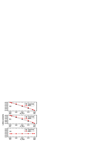
Note that the lattice mismatch between ZnO (MgO) and BeO is 19.6% (19.9%). Consequently, the ZnBeO and MgBeO alloys are highly strained and the lattice constants may deviate from the Vegard law. First, we calculate the lattice constant by the Vegard law, then fit the Murnaghan equation of stater24 at various lattice constants around it. Figure 1 shows the lattice constant as a function of concentration x obtained from the Vegard law (black dots) and fitted by the Murnaghan equation (red dots). We note that (i) For the ZnBeO and MgBeO alloys, due to the large size difference between the Zn (Mg) and Be atom, the lattice constants calculated by LDA (by fitting the Murnaghan equation) are slightly larger than those obtained from the Vegard law. This is because the Zn-O (Mg-O) bond is hard to compress. Our calculated results also show that nearly all the Be-O bonds are longer than those of Be-O in the host BeO. The biggest deviation occurring at composition x=0.5 is 2.5% for ZnBeO alloys. (ii) the Vegard law is a good model for ZnMgO alloys due to the lattice match and the similar size of Zn and Mg ions. In actuality, we use the lattice constants obtained by fitting the Murnaghan equation in all our calculations for ternary alloys.
III.2 The bowing parameters b of ZnMgO, ZnBeO, and MgBeO alloys
We calculate the LDA band gaps to be 0.70, 3.731, 7.852 eV at point for zinc-blende ZnO, MgO and BeO, respectively. Due to the LDA underestimation of band gap, our values are smaller than the experimental valuesr7 of 3.4, 7.67, 10.585 eV for their ground-state phase, respectively. However, the error of bowing parameter b is small in Eq. 1 because the systematic band gap error cancels out in deriving the bowing parameters through comparing chemically identical systems in two different forms (AX and BX)r25 . This has been confirmed by numerous studiesr9 ; r25 .
Table II presents the calculated band-gap bowing coefficients for Mg1-xBexO, Zn1-xBexO and Zn1-xMgxO ternary alloys as a function of the composition x. our results show some chemical trends.
| composition x | |||||
|---|---|---|---|---|---|
| Ternary Alloys | 0.0625 | 0.25 | 0.50 | 0.75 | 0.9375 |
| Zn1-xMgxO | 0.8794 | 0.9797 | 1.4172 | 2.2827 | 4.3430 |
| Zn1-xBexO | 4.8215 | 5.8189 | 8.2116 | 12.8925 | 23.9648 |
| Mg1-xBexO | 4.4951 | 5.2883 | 5.4772 | 7.2861 | 18.0994 |
(i) The bowing parameters b are large for ZnBeO and MgBeO alloys. This is thought to be because of the atomic size difference and the large chemical mismatch between Zn (Mg) and Be. However, compared with ZnBeO and MgBeO the bowing parameters of ZnMgO alloys are smaller as Zn and Mg are of similar size. The atomic size of Zn is a little larger than that of Mg, thus the bowing parameters of ZnBeO are also a little larger that those of MgBeO. From Be to Mg to Zn, the atomic size difference increases as does the atomic p-orbital energy difference.
(ii) The bowing parameters are composition and large at Be-rich region for ZnBeO and MgBeO alloys. Taking ZnBeO as an example, the bowing parameter b is 4.8215 eV in the Zn-rich region, whereas in the Be-rich region the b is 23.9648 eV. This is because the size and chemical differences between Zn and Be are large. Incorporation of a small amount of Zn into BeO at substitutional sites creates a deep isovalent defect level inside the band gap. Our direct calculations show that the position of the isovalent defect level is at 0.66 eV below the conduction band minimum (CBM). Furthermore the VBM is pushed up due to the p-d repulsion introduced by Zn 3d orbital. This leads to a large band-gap reduction and a large bowing parameter in the Be-rich region. However, upon adding a small amount of Be into ZnO, the VBM will shift downwards by a small amount due to the reduction in p-d repulsion. In this case the band gap increases a little and the bowing parameter is small.
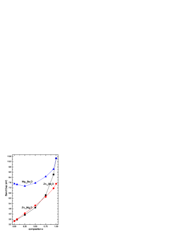
(iii) Using the bowing parameters and experimental band gaps, we calculate the band gaps of ZnBeO, MgBeO, and MgBeO alloys at different concentrations. The results are summarized in Figure 2. We notice that although the band gap of BeO is larger than that of MgO, incorporation of a small amount of Be into the MgO matrix will lead to a reduction in the band gap, indicating that the bowing parameter is larger than the band-gap difference. For Mg0.75Be0.25O, the bowing parameter b (5.2883 eV) is larger that the band gap difference (2.915 eV).
III.3 The formation energies and transition energy levels of N in ZnBeO and ZnMgBeO quaternary alloys
P-type doping of ZnO is difficult due to the low VBM resulting from the largely electronegative characteristic of oxygen. In order to lower the acceptor ionization energy extensive studies have been performed. Park et al.r10 showed that N is the best p-type dopant source among the group-I and V elements. Li et al.r11 also showed that replacing Zn with Mg or Be surrounding the NO substitutional defect can decrease the acceptor transition level. In the ZnBeO ternary alloy, it is easy to form NO+nBeZn complexes; thus we expect the acceptor transition level becomes shallower when the NO is surrounded by more Be atoms. In the following study, we choose the Zn0.75Be0.25O alloy approximately as the experimental investigations dor5 , and we also choose the N as dopant due to its low valence p-orbital energy.
The ionization energy of an accepter (q0) with respect to the VBM in the impurity limit is calculated by the following procedure, further described in Refs. 26 and 27,
| (3) | |||||
where and are the total energies of the supercell at charge state and neutral, respectively, for defect , and are the defect levels at the special points (averaged) and at the point, respectively, and (host) is the VBM energy of the host supercell at the point and is aligned using core electron levels away from the defect. The first term on the right-hand side of Eq. (5) determines the U energy parameter (including both the Coulomb contribution and atomic relaxation contribution) of the charged defects calculated at the special k points, which is the extra cost of energy after moving (-q) charge from the VBM of the host to the neutral defect level. The second term gives the single-electron defect level at the point. For charged defects, a uniform background charge is added to retain the global charge neutrality of the periodic unit-cell.
The defect formation energy of a neutral defect is defined as
| (4) |
where E(host) is the total energy of the host supercell without defect ; and are the chemical potentials of constituents O and (N) relative to the element gas energy. The (0) and (0) are the numbers of O and extrinsic defects (N). We calculate the chemical potentials for O() and N(), relative to gaseous O2 and N2.
Table III shows our calculated NO acceptor formation energies and (0/-) transition energy levels for the ZnO and Zn0.75Be0.25O alloy. For N in Zn0.75Be0.25O alloy, we calculate the NO at different sites. The nNN in Table III denotes that there are n Be atoms in the tetrahedral nearest neighbor (NN) sites centered around the N atom. Our calculated results show the following typical behaviours.
| Hf(,0) | (0/-) | |
|---|---|---|
| 0NN | 4.793 | 0.533 |
| 1NN | 4.818 | 0.347 |
| 2NN | 5.134 | 0.233 |
| ZnO | 4.661 | 0.362 |
(i) The formation energy of neutral NO defect in the Zn0.75Be0.25O alloy increases when there are larger numbers of Be atoms in the defect neighboring sites. This is because the NO substitution introduces a larger strain into the Be-rich region than into the Zn-rich region. The formation energy of NO in the ZnO is smaller than that in the alloy. This is because the volume of ZnO is about 0.9% greater than that of the Zn0.75Be0.25O alloy, indicating that an NO defect in pure ZnO introduces a smaller strain.
(ii) For NO in ZnO, our calculated NO (0/-) acceptor level is at 0.362 eV above the VBM, which agrees well with previous first-principles calculationsr10 ; r11 . For the case of the Zn0.75Be0.25O alloy, we note that the position of NO (0/-) acceptor level is dependent on the site of the defect. It decreases as the number of N nearest neighbouring atoms increases, from 0.533 eV when N has no nearest neighboring (0NN) Be atoms to 0.233 eV when there are 2 NN Be atoms. This is thought to be because the acceptor level is lowered by the reduction in the p-d repulsion. A more detailed explanation is presented. For ZnO, the VBM state consists mostly of pO, pZn, and dZn orbitals. For an NO acceptor in ZnO, the defect level mainly consists of N impurity valence p orbitals, and the acceptor level is pushed up by the p-d (pN-dZn) repulsion introduced by the same symmetry. However, for Be, it has no occupied 2p and 3d orbitals. If Zn is substituted by Be, the p-d (pN-dZn) repulsion will decreases and the NO acceptor transition level becomes shallow. We also note that the p-p repulsion can push the acceptor level further down, although it is weaker compared with p-d repulsion because the p-p (p-d) repulsion is inversely proportional to the energy difference between the pN and pBe (pN and dZn) valence orbitalsr280 . Similarly, in the Zn0.75Be0.25O alloy, from 0NN to 2NN, the pN-dZn repulsion decreases and the p-p (pN-pBe) repulsion increases; thus, the NO acceptor level becomes increasingly shallower. In 0NN, the NO acceptor level in the Zn0.75Be0.25O alloy is deeper than that in ZnO due to the lower VBM (see below).
(iii) According to Eq. 4, we see that the chemical potentials have large effect on the defect formation energy. Practically, the chemical potentials can vary in a range because of some thermodynamic limitsr29 . The high defect formation energy leads to a low dopant solubility, which may be overcome by non-equilibrium growth methodsr29 . If the formation energy of NO in Zn0.75Be0.25O alloy is reduced so that it is smaller than that in ZnO by controlling the chemical potentials of N and O during the growth process, there are more N atoms residing in the 1NN and 2NN sites with low acceptor transition levels. Based on this, we predict that ZnBeO alloy may be a better p-type doping material than ZnO.
We have also investigated the electronic structures and p-type doping properties of the ZnMgBeO quaternary alloy lattice-matched to GaN substrate. For quaternary alloys, the band gap and lattice constant can be individually tuned. For Zn1-x-yMgyBexO alloy, the lattice constant can be described by
| (5) |
For the Zn22Mg8Be2O32 alloy, we find the Vegard law is well obeyed. We also note that the lattice constants of Zn22Mg8Be2O32 quaternary alloy and zinc-blende GaN are 4.461 and 4.462 År30 , respectively, thus the lattices match well.
The band gap of the Zn1-x-yMgyBexO quaternary alloys is a function of compositions x and y and can be described by a second order expansion in x and yr301 ,
| (6) | |||||
In order to get bxy approximately, we use the SQS at (x,y)=(0.0,0.5),(0.5,0.0), and (0.5,0.5). The parameter bxy is obtained using bxy=bZnBeO-bZnMgO-bMgBeO under a quadratic approximation. Our calculated bxy is 1.317 eV. Using the experimental band gaps and Eq. 6, we predict that the band gap of Zn22Mg8Be2O32 alloy is 4.149 eV.
Table IV shows calculated NO acceptor formation energies and (0/-) transition energy levels for Zn22Mg8Be2O32 alloy. The nNN in Table IV denotes that there are n Mg atoms in the tetrahedral nearest neighbor (NN) sites centered around the N atom. The 0NN1Be denotes that N atom has one Be atom and without Mg atoms in the NN sites. From 0NN to 3NN, the (0/-) decreases slightly less than that of the Zn0.75Be0.25O alloy. This is because the pMg orbital energy level is higher than that of pBer280 , thus the p-p repulsion pushing down the acceptor level is weaker in the quaternary alloy. The (0/-) is smaller in 0NN1Be than that in 0NN, which is also consistent with our findings for NO in the Zn0.75Be0.25O alloy. We note that the NO (0/-) transition energy level is deeper than that in ZnO because of the large downward shift of the VBM according to our band alignment calculation (see below). The CMB of Zn22Mg8Be2O32 alloy is as low as that of ZnO, indicating that it is also can be n-type doped easily.
| Hf(,0) | (0/-) | |
|---|---|---|
| 0NN | 4.773 | 0.546 |
| 1NN | 5.176 | 0.489 |
| 2NN | 5.611 | 0.458 |
| 3NN | 6.033 | 0.446 |
| 0NN1Be | 4.978 | 0.477 |
IV The natural valence band alignment
Band offset is an important parameter in the heterostructures. We shall describe how we investigated the natural band alignment by adopting the approach proposed by Weir31 . This method is also widely used in photoemission core level spectroscopyr32 . According to Wei’s methodr31 , the band offset is given by
| (7) |
Here,
| (8) |
(and similarly for ) are the energy separations between core level (C) and valence band maximum energy for pure AX (and similarly for pure BY), while
| (9) |
is the difference in core level binding energy between AX and BY at the AX/BY superlattice. We calculate the and at the equilibrium zinc-blende lattice constants for AX and BY, respectively. We use the average lattice constant (between AX and BY) to calculate the in the AX/BY superlattice. A more detailed description of the procedure can be found in Ref. 32.
The natural conduction band minimum (CBM) alignment is calculated by
| (10) |
where is the experimental band gap difference between the AX and BY alloys.

Our calculated natural band alignment is shown in Fig. 3. For the VBM alignment, the VBM of ZnO is higher than that of MgO and BeO. This is because the p-d () repulsion pushes up the VBM, whereas Mg and Be have no active d electrons. According to the common-anion ruler31 , the valence band offset is small between common-anion systems. However, the VBM of BeO is higher than that of MgO. This is because BeO shows strong covalency, resulting in the kinetic-energy-induced valence band broadeningr33 . If we assume that the VBM varies linearly as a function of the alloy composition, Zn24Be8O32 would have a VBM approximately 0.32 eV lower than that of ZnO. However, our direct calculation shows that VBM of Zn24Be8O32 (Zn0.75Be0.25O) alloy is only about 0.11 eV lower than that of ZnO due to the large p-d repulsion. In order to investigate the natural conduction band alignment, we use the experimental band gaps demonstrated in Fig. 3. We see that the Zn0.75Be0.25O alloy acts as a good barrier material for ZnO-based UV LEDs. The and have values of approximately 0.60 and 0.11 eV, respectively, which are large enough to strongly confine the electrons and holes wellr34 . The quaternary alloy Zn22Mg8Be2O32 has a CBM as low as that of ZnO, indicating that it can be n-type doped easily. By contrast p-type doping is more difficult due to the low VBM which is also confirmed by our study of p-type doping above. Based on these chemical behaviours, we can tailor the band offset to practically perform the band-engineering as desired. We hope that our results will be helpful for the applications of optoelectronic devices.
V SUMMARY
We have investigated the band gap bowing parameters and p-type doping properties of (Zn, Mg, Be)O related random ternary and quaternary alloys using first-principles band-structure methods. The bowing parameters are large and dependent on composition for ZnBeO and MgBeO alloys due to their large size and chemical mismatch. We also show that the band gap of MgO will reduce on adding a small amount of Be into MgO. The acceptor transition energy level becomes shallower when N has more Be nearest neighbors, thus ZnBeO (Zn0.75Be0.25O) may be a good p-type material. The electronic and p-type doping properties of ZnMgBeO quaternary alloy lattice-matched to GaN substrate are also studied. According to our natural band alignment calculations, n-type doping of Zn22Mg8Be2O32 should be easy due to the low CBM. We hope our conclusions have applications to optoelectronic devices.
Acknowledgements.
This work was supported by the National Basic Research Program of China (973 Program) grant No. G2009CB929300 and the National Natural Science Foundation of China under Grant Nos. 60521001 and 60776061.References
- (1) A. Schleife, F. Fuchs, J. Furthmuller, F. Bechstedt, Phys. Rev. B 73, 245212 (2006)
- (2) Y. Duan, H. Shi, L. Qin, Phys. Lett. A 372, 2930 (2008)
- (3) H. Shi, Y. Duan, J. Appl. Phys. 103, 073903 (2008)
- (4) Y. R. Ryu, T. S. Lee, J.A. Lubguban, A. B. Corman, H. W. White, J. H. Leem, M. S. Han, Y. S. Park, C. J. Youn, W. J. Kim, Appl. Phys. Lett. 88, 052103 (2006)
- (5) Y. R. Ryu, T. S. Lee, J. A. Lubguban, H. W. White, B. J. Kim, Y. S. Park, C. J. Youn, Appl. Phys. Lett. 88, 241108 (2006)
- (6) Y. R. Ryu, J. A. Lubguban, T. S. Lee, H. W. White, T. S. Jeong, C. J. Youn, B. J. Kim, Appl. Phys. Lett. 90, 131115 (2007)
- (7) Semiconductors: Data Handbook, 3rd Ed., edited by O. Madelung (Springer, Berlin, 2004)
- (8) S.-H. Wei, A. Zunger, Phys. Rev. Lett. 76, 664 (1996); L. Bellaiche, S.-H. Wei, A. Zunger, Phys. Rev. B 54, 17568 (1996)
- (9) C.-Y. Moon, S.-H. Wei, Y. Z. Zhu, G. D. Chen, Phys. Rev. B 74, 233202 (2006)
- (10) C. H. Park, S. B. Zhang, S.-H. Wei, Phys. Rev. B 66, 073202 (2002)
- (11) J. Li, S.-H. Wei, S. S. Li, J. B. Xia, Phys. Rev. B 74, 081201(R) (2006)
- (12) Y. Yan, J. Li, S.-H. Wei, M. M. Al-Jassim, Phys. Rev. Lett. 98, 135506 (2007)
- (13) W. Kohn, L. J. Sham, Phys. Rev. 140, A1133 (1965)
- (14) G. Kresse, J. Furthmuller, Phys. Rev. B 54, 1116 (1996)
- (15) G. Kresse, D. Joubert, Phys. Rev. B 59, 1758 (1999)
- (16) H. J. Monkhorst, J. D. Pack, Phys. Rev. B 13, 5188 (1972)
- (17) A. Zunger, S.-H. Wei, L. G. Ferreira, J. E. Bernard, Phys. Rev. Lett. 65, 353 (1990)
- (18) S.-H. Wei, L. G. Ferreira, J. E. Bernard, A. Zunger, Phys. Rev. B 42, 9622 (1990)
- (19) C.Y. Yeh, S.-H Wei, A. Zunger, Phys. Rev. B 50, 2715 (1994)
- (20) K. J. Chang, S. Froyen, M. L. Cohen, J. Phys. C: Solid State Phys. 16, 3475 (1983);S. Limpijumnong, S. B. Zhang, S.-H. Wei, C. H. Park, Phys. Rev. Lett. 92, 155504 (2004)
- (21) A. B. M. A. Ashrafi, A. Ueta, H. Kumano, I. Suemune, Y.-W. Ok, T.-Y. Seong, Appl. Phys. Lett. 79, 470 (2001)
- (22) J. C. Boettger, J. M. Wills, Phys. Rev. B 54, 8965 (1996)
- (23) L. Vegard, Z. Phys. 5, 17 (1921)
- (24) F. D. Murnaghan, Proc. Natl. Acad. Sci. U.S.A. 30, 244 (1944)
- (25) S.-H Wei, S. B. Zhang, A. Zunger, J. Appl. Phys. 87, 1304 (2000)
- (26) S.-H. Wei, S. B. Zhang, Phys. Rev. B 66, 155211 (2002)
- (27) S.-H. Wei, Comput. Mater. Sci. 30, 337 (2004)
- (28) Our calculated (semi-relativistic) atomic LDA valence orbital energies for -, - and - are -5.137, 3.181 and 0.728 eV, respectively.
- (29) S. B. Zhang, S.-H. Wei, Phys. Rev. Lett. 86, 1789 (2001)
- (30) H. Shi, Y. Duan, Phys. Lett. A 373, 165 (2008)
- (31) F. Wang, S. S. Li, J. B. Xia, H. X. Jiang, J. Y. Lin, J. Li, S.-H. Wei, Appl. Phys. Lett. 91, 061125 (2007)
- (32) S.-H. Wei, A. Zunger, Appl. Phys. Lett. 72, 2011 (1998)
- (33) S. P. Kowalczyk, J. T. Cheung, E. A. Kraut, R. W. Grant, Phys. Rev. Lett. 56, 1605 (1986)
- (34) D. Segev, S.-H. Wei, Phys. Rev. B 68, 165336 (2003)
- (35) M. Kondow, K. Uomi, A, Niwa, T. Kitatani, S. Watahiki, Y. Yazawa, Jpn. J. Appl. Phys. 35, 1273 (1996)