Film-thickness dependence of 10 GHz Nb coplanar-waveguide resonators
Abstract
We have studied Nb
coplanar-waveguide (CPW) resonators
whose resonant frequencies are GHz.
The resonators have different film thicknesses,
0.1, 0.2, and 0.3 m.
We measured at low temperatures, K,
one of the scattering-matrix element, ,
which is the transmission coefficient from one port to the other.
At the base temperatures, K,
the resonators are overcoupled to
the input/output microwave lines,
and the loaded quality factors are on the order of
.
The resonant frequency has a considerably larger film-thickness
dependence compared to the predictions
by circuit simulators
which calculate the inductance of CPW
taking into account only,
where is the usual magnetic inductance
determined by the CPW geometry.
By fitting a theoretical
vs. frequency curve
to the experimental data,
we determined for each film thickness,
the phase velocity of the CPW
with an accuracy better than 0.1%.
The large film-thickness dependence must be due to
the kinetic inductance of the CPW center conductor.
We also measured
as a function of temperature up to K,
and confirmed
that both thickness and temperature dependence are
consistent with the theoretical prediction
for .
J. Vac. Sci. Technol. B 27, 2286 (2009)
[DOI: 10.1116/1.3232301]
I Introduction
Microwave resonators (for example, Chap. 7 of Ref. Pozar, 1990) are one of the key components in a variety of circuits operated at GHz frequencies, and their new applications continue to emerge. A simple example is band-pass filters, which are based on the fact that the microwave transmission through resonators is frequency sensitive. The same idea is also used for more complex devices, such as oscillators, tuned amplifiers, and frequency meters. Actually, having high-quality filters and oscillators is critical in mobile communications, where available bands keep getting overcrowded as demand grows rapidly.
Another application of microwave resonators is radiation detectors, which often consist of sensor heads and read-out circuits, and resonators can be used in the readout circuit. When one would like to detect at the single-photon level, one needs to have detectors with high enough energy resolutions. In this respect, superconducting sensor headsIrwin (1995); Peacock et al. (1996); Gol’tsman et al. (2001) can be advantageous, and may be the only solution at present depending on the energy range of the object. Once one decides to use superconducting sensor heads, it makes sense to fabricate the read-out circuit with superconducting materials as well. Superconducting microwave resonators allow one to obtain higher quality factors, which are favorable for frequency multiplexing. In addition, one type of photon detector is designed to probe the change in the kinetic inductance of superconducting thin-film resonator due to the absorbed photons.Mazin et al. (2002) In this device concept, the resonator works as a sensor head rather than a part of the readout circuit.
Recently, superconducting resonators are used for the nondemolition readout of superconducting qubits as well.Wallraff et al. (2004) Since the demonstration by Wallraff et al.,Wallraff et al. (2004) this type of readout scheme has been one of the main topics in the field of superconducting qubits, and we are also developing a similar readout technique.Inomata et al. (2009) In superconducting resonators, kinetic inductance, which is essentially the internal mass of the current carriers, plays an important role especially when the superconducting film is thin. In our circuit,Inomata et al. (2009) for example, a Nb coplanar-waveguide (CPW) resonator is terminated by an Al dc SQUID, and the total thickness of the Al layers is 0.04 m. In order to avoid a discontinuity at the Al/Nb interface, we usually choose the Nb thickness to be 0.05 m, which is much thinner than a typical thickness of 0.3 m for superconducting integrated circuits fabricated by the standard photolithographic technology. Fabricating circuits with thinner films is actually important from the viewpoint of miniaturization as well. Therefore, for designing resonators, quantitative understanding of the kinetic inductance in the CPW is important.
There have been a number of reports on kinetic inductance for a variety of materials.Meservey and Tedrow (1969); Rauch et al. (1993); Kisu et al. (1993); Watanabe et al. (1994); Gubin et al. (2005); Frunzio et al. (2005) In general, however, kinetic inductance is indirectly measured by assuming a theoretical model, and as a result, the uncertainties are relatively large. Thus, although kinetic inductance is a well established notion and the phenomenon is qualitatively understood, the quantitative information is not necessarily sufficient from the point of view of applications, especially at high frequencies, 10 GHz. When we would like to precisely predict the resonant frequency, the best solution would be to characterize the actual CPW in a simple circuit. Such characterization should also improve the knowledge of superconducting microwave circuits. Very recently, Göppl et al.Göppl et al. (2008) measured a series of Al CPW resonators with nominally the same film thickness of 0.2 m, and investigated the relationship between the loaded quality factor at the base temperature of 0.02 K and the coupling capacitance. For this purpose, it is justified to neglect kinetic inductance because the kinetic inductance should be the same in their resonators and estimatedGöppl et al. (2008) to be about two orders of magnitude smaller than the usual magnetic inductance determined by the CPW geometry. In this work, on the other hand, we paid close attention to the resonant frequency as well, and characterized Nb CPW resonators as a function of film thickness rather than a function of coupling capacitance. We also looked at the temperature dependence in order to discuss kinetic inductance in detail.
II Experiment
| Reso- | |||||
|---|---|---|---|---|---|
| nator | (m) | (GHz) | (103) | (fF) | (%) |
| A1 | 0.05 | 10.01 | 1.6 | 7.00.4 | 39.310.03 |
| A2 | 0.1 | 10.50 | 1.4 | 7.30.4 | 41.280.04 |
| A3 | 0.2 | 10.74 | 1.4 | 7.20.4 | 42.210.04 |
| A4 | 0.3 | 10.88 | 1.6 | 6.60.4 | 42.710.03 |
| B1 | 0.05 | 10.06 | 3.4 | 4.60.3 | 39.320.02 |
| B2 | 0.1 | 10.56 | 3.1 | 4.80.3 | 41.260.02 |
| B3 | 0.2 | 10.81 | 2.7 | 5.00.3 | 42.270.03 |
| B4 | 0.3 | 10.94 | 3.3 | 4.50.3 | 42.720.02 |

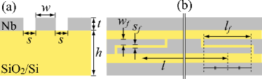
We studied two series of Nb CPW resonators listed in Table 1. Each resonator consists of a section of CPW and coupling capacitors, as shown schematically in Fig. 1. The resonators were fabricated on a nominally undoped Si wafer whose surface had been thermally oxidized. On the SiO2/Si substrate, a Nb film was deposited by sputtering and then patterned by photolithography and SF6 reactive ion etching. Figure 2(a) represents the cross section of CPW. The center conductor has a width of m, and separated from the the ground planes by m, so that the characteristic impedance becomes . The thickness of Nb is , 0.1, 0.2, or 0.3 m (see Table 1), and that of SiO2/Si substrate is m. The SiO2 layer, whose thickness is 0.3 m, is not drawn in Fig. 2(a). We employed interdigital coupling capacitors as shown in Fig. 2(b). The finger width is m, the space between the fingers is m, and the finger length is m for Resonators A1–A4 and m for Resonators B1–B4. Here, we quoted designed dimensions for the Nb structures. The actual dimensions differ by about 0.2 m due to over-etching; for example, and are m smaller, whereas and are m larger. In this paper, we define the resonator length as the distance between the center of the fingers on one side and that on the other side, and mm for all resonators. Because our chip size is 2.5 mm by 5.0 mm, our CPWs meander as in Fig. 3.
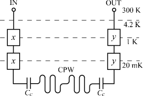
The resonators were measured in a 3He-4He dilution refrigerator at K. A typical measurement setup is shown schematically in Fig. 3. The boxes in the figure represent attenuators. The amount of attenuation was not the same because the microwave lines in our refrigerator had been designed for several different purposes. The attenuation was dB for Resonators A2, B3, and B4, and dB for the others; dB for all resonators except A1 and A3. For Resonators A1 and A3, we used a line with no attenuators ( dB) but with an isolator and a cryogenic amplifier at 4.2 K. The gain of the cryogenic amplifier was 40 dB for Resonator A1 and 34 dB for A3. We measured the transmission coefficient by connecting a vector network analyzer to the “IN” and “OUT” ports in Fig. 3. A typical incident power to the resonator was dBm. For each resonator, we confirmed that the measurements were done in an appropriate power range in the sense that the results looked power independent.
III Results
III.1 at the base temperatures
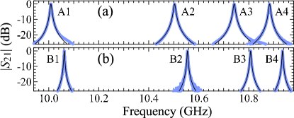
Figure 4 shows the amplitude of at the base temperatures, K, as a function of frequency for all resonators. The resonant frequency has a rather large film-thickness dependence. Our interpretation is that this is due to the kinetic inductance of the CPW center conductor. Before discussing the thickness dependence in detail, let us look at the quality factors.
What we obtain by measuring as a function of is the loaded quality factor , which is related to the external quality factor and the unloaded quality factor by
| (1) |
In general, is determined mainly by , whereas is a measure of the internal loss, which arises not only from the dielectric but also from the superconductor in the high-frequency regime. Our resonators should be highly overcoupled to the input/output lines at the base temperatures, that is, , and thus, . As listed in Table 1, of our resonators is on the order of 103. These values are not only reasonable for the designs of our finger-shaped coupling capacitors but also much smaller than typical values of below 0.1 K for superconducting microwave resonators.Mazin et al. (2002); Frunzio et al. (2005); Göppl et al. (2008) When , the maximum is expected to be 0 dB. We have confirmed by taking into account attenuators, amplifiers, and cable losses, that our measurements are indeed consistent within the uncertainties of gain/loss calculations, 1–2 dB. Based on this confirmation, the experimental data in Fig. 4 are normalized so that the peak heights equal 0 dB.
The solid curves in Fig. 4 are calculations based on the transmission () matrix (for example, Sec. 5.5 of Ref. Pozar, 1990), and they reproduce the experimental data well. The matrix for the resonators is given by
| (2) |
where
| (3) |
is the imaginary unit,
| (4) |
for lossless CPWs, , ,
| (5) |
is the phase velocity, which is strongly related to ,
| (6) |
is the characteristic impedance, is the inductance per unit length, and is the capacitance per unit length. From these transmission-matrix elements, the scattering-matrix elements are calculated, and is given by
| (7) |
where is the characteristic impedance of the microwave lines connected to the resonator. Unit-length properties of CPW are determined when two parameters out of , , , and are specified. In the calculations for Fig. 4, we employed F/m based on the considerations described in the following paragraph, and evaluated and by least-squares fitting.
WenWen (1969) calculated CPW parameters using conformal mapping. Within the theory, does not depend on , and it is given by
| (8) |
where is the relative dielectric constant of the substrate, F/m is the permittivity of free space, is the complete elliptical integral of the first kind, the argument is given by
| (9) |
and For our CPWs, we obtain F/m when we employ for Si (p. 223 of Ref. Kittel, 1996) neglecting the contribution from the SiO2 layer, which is much thinner compared to , , or . Circuit simulators [Microwave Office from AWR (#1) and AppCAD from Agilent (#2)] also predict similar values of . The simulators calculate CPW parameters from the dimensions and the material used for the substrate. The predictions by the simulators have dependence, but in the relevant range, the variations are on the order of 1% or smaller as summarized in Table 2, and the values of are between F/m and F/m. Thus, partly for simplicity, we used F/m for all of our resonators.
| (%) | (%) | |||||
|---|---|---|---|---|---|---|
| (m) | #1 | #2 | #1 | #2 | A | B |
| 0.05 | 1.7 | 3.9 | 2.9 | 18.0 | 18.0 | |
| 0.1 | 1.4 | 3.0 | 2.2 | 7.1 | 7.2 | |
| 0.2 | 0.8 | 1.4 | 1.2 | 2.4 | 2.1 | |
With F/m, the values of in Table 1 correspond to , which agrees with our design of . We have done the same fitting by changing the value of by as well in order to estimate the uncertainties, which are also listed in Table 1. Within the uncertainties, the values of from the same coupling-capacitor design agree, and fF for Resonators A1–A4 with m and fF for Resonators B1–B4 with m. The uncertainties for is much smaller, , and again within the uncertainties, the values of for the same agree.
For the rest of this paper, let us assume that dependence of is negligible. This assumption is consistent with the fact that the experimental vs. in Table 1 does not show any obvious trend. Moreover, according to the circuit simulators in Table 2, dependence of is smaller than that of . Below, we look at mainly instead of or other CPW parameters so that we will be able to discuss the kinetic inductance. As long as we deal with a normalized inductance such as the ratio of to , what we choose for the value of does not matter very much because obtained from the fitting was not so sensitive to . Hence, we analyze the quantities obtained with F/m only hereafter. In Table 2, we list the variations of in our two series of resonators as well. For both series, the magnitude of the variations are much larger than the predictions by circuit simulators. We will discuss this large dependence in terms of kinetic inductance in Sec. IV after examining the temperature dependence in Sec. III.2.
III.2 Temperature dependence of
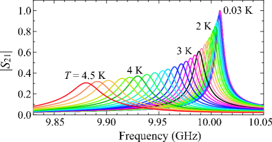
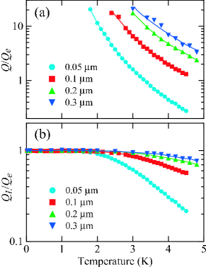
We also measured vs. at various temperatures up to K for Resonators A1–A4. We show the results for Resonator A1 in Fig. 5. With increasing temperature, , , and the peak height decrease. As in Sec. III.1, let us look at the quality factors first. In our resonators, at the base temperatures as we pointed out in Sec. III.1. Thus, when we assume that is temperature independent, we can calculate from measured using Eq. (1). We plot and vs. in Fig. 6 for all of the four resonators. With increasing temperature, decreases in all resonators. A finite means that the resonator has a finite internal loss, which is consistent with a peak height smaller than unity in Fig. 5. The internal loss at high temperatures must be due to quasiparticles in the superconductor, as discussed in Ref. Mazin et al., 2002. The reduction of quality factors becomes larger as the Nb thickness is decreased. At K, however, the reduction is negligibly small, and thus, in this sense, it should be fine to choose any thickness in the range of m for the study of superconducting qubits that we mentioned in Sec. I because qubit operations are almost always done at the base temperatures.
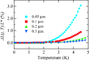
When CPWs are no longer lossless, in Eq. (4) has to be replaced by . This characterizes the internal loss, and is equal to (for example, Sec. 7.2 of Ref. Pozar, 1990). From similar calculations to those in Sec. III.1, we evaluated at higher temperatures as well by neglecting the dependence of and . Because we are interested in the temperature variation of , we show vs. in Fig. 7, where , is the base temperature, and . The variation becomes larger as the Nb thickness is decreased. This trend also suggests that we should take into account the kinetic inductance.
IV Discussion
The film-thickness and temperature dependence that we have examined in Sec. III is explained by the model,
| (10) |
where is the usual magnetic inductance per unit length determined by the CPW geometry and is the kinetic inductance of the CPW center conductor per unit length. We neglect the contribution of the ground planes to because the ground planes are much wider than the center conductor in our resonators [see Eq. (11)]. We also assume that depends on only, whereas does on both and . This type of model has been employed in earlier worksRauch et al. (1993); Frunzio et al. (2005); Göppl et al. (2008) as well. The dependence of arises from the fact that is determined not only by the geometry but also by the penetration depth , which varies with . Meservey and TedrowMeservey and Tedrow (1969) calculated of a superconducting strip, and when the strip has a rectangular cross section like our CPWs, is written as
| (11) |
where H/m is the permeability of free space. The relationship between and is expressed in a much simpler form in the thick- and thin-film limits; for , and for . When we assume Eqs. (10) and (11), we obtain numerically, once is given. Below, we discuss in our Nb films in order to confirm that the model represented by Eq. (10) is indeed appropriate.
| (m) | (%) | (%) |
|---|---|---|
| 0.05 | 4.3 | 13.1 |
| 0.1 | 3.4 | 4.9 |
| 0.2 | 1.7 | 2.2 |
| 0.3 | – | 1.6 |
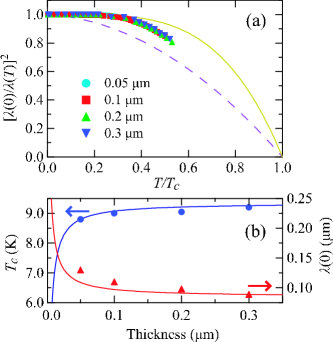
In Fig. 8(a), we plot vs. for Resonators A1–A4, where is the superconducting transition temperature, which is assumed to be also dependent in this paper. We have found that with a reasonable set of parameters, and , the experimental data for all resonators are described by a single curve. This kind of scaling is expected theoretically in the limits of and , where is the coherence length and is the London penetration depth.Tinkham (1996) Although in Nb (p. 353 of Ref. Kittel, 1996) at temperatures well below , it would be still reasonable to expect a scaling in our Nb resonators because at a given normalized temperature , the relevant quantities should be on the same order of magnitude in all resonators, and thus, two parameters, and , are probably enough for characterizing of our resonators. The values of and employed in Fig. 8(a) are summarized in Table 3 and Fig. 8(b), respectively. The relative change of in Table 3 is similar to the predictions by circuit simulators in Table 2, which do not take into account the kinetic inductance. The magnitude of is also reasonable because for all thickness. In Table 3, we also list the ratio of kinetic inductance to the total inductance . With decreasing thickness, indeed increases rapidly. In Fig. 8(b), and are plotted together with the theoretical curves in Figs. 1 and 6 of Ref. Gubin et al., 2005, where Gubin et al.Gubin et al. (2005) determined some parameters of the curves by fitting to their experimental data. The values of are reasonable, and is on the right order of magnitude.
The solid curve in Fig. 8(a) is the theoretical dependence based on the two-fluid approximation,Tinkham (1996)
| (12) |
This theoretical curve reproduces the experimental data at , when we assume that in Resonators A1–A4. At , on the other hand, the experimental data deviate from Eq. (12), but according to Ref. Tinkham, 1996, the expression for vs. depends on the ratio of , and thus, Eq. (12) cannot be expected to apply to all materials equally well. Indeed, although the temperature dependence of Eq. (12) has been observed in the classic pure superconductors,Tinkham (1996) such as Al with at temperatures well below , it does not seem to be the case in the high- materials, whose typical is in the opposite limit,Tinkham (1996) , and for example, Rauch et al.Rauch et al. (1993) employed for a high- material YBa2Cu3O7-x, an empirical expression of
| (13) |
which is the broken curve in Fig. 8(a), instead. Because in Nb even at , and because the experimental data at are between Eqs. (12) and (13), we believe that the deviation from Eq. (12) at is reasonable.
From the discussion in this section, we conclude that the model represented by Eq. (10) explains the film-thickness and temperature dependence of our resonators.
V Conclusion
We investigated two series of Nb CPW resonators with resonant frequencies in the range of GHz and with different Nb-film thicknesses, m. We measured the transmission coefficient as a function of frequency at low temperatures, K. For each film thickness, we determined the phase velocity in the CPW with an accuracy better than 0.1% by least-squares fitting of a theoretical curve based on the transmission matrix to the experimental data at the base temperatures. Not only the film-thickness dependence but also the temperature dependence of the resonators are explained by taking into account the kinetic inductance of the CPW center conductor.
Acknowledgment
The authors would like to thank Y. Kitagawa for fabricating the resonators, and T. Miyazaki for fruitful discussion. T. Y., K. M., and J.-S. T. would like to thank CREST-JST, Japan for financial support.
References
- Pozar (1990) D. M. Pozar, Microwave Engineering (Addison-Wesley Publishing Company, Inc., Reading, Massachusetts, 1990).
- Irwin (1995) K. D. Irwin, Appl. Phys. Lett. 66, 1998 (1995).
- Peacock et al. (1996) A. Peacock, P. Verhoeve, N. Rando, A. V. Dordrecht, B. G. Taylor, C. Erd, M. A. C. Perryman, R. Venn, J. Howlett, D. J. Goldie, et al., Nature 381, 135 (1996).
- Gol’tsman et al. (2001) G. N. Gol’tsman, O. Okunev, G. Chulkova, A. Lipatov, A. Semenov, K. Smirnov, B. Voronov, A. Dzardanov, C. Williams, and R. Sobolewski, Appl. Phys. Lett. 79, 705 (2001).
- Mazin et al. (2002) B. A. Mazin, P. K. Day, H. G. LeDuc, A. Vayonakis, and J. Zmuidzinas, Proc. SPIE 4849, 283 (2002).
- Wallraff et al. (2004) A. Wallraff, D. I. Schuster, A. Blais, L. Frunzio, R.-S. Huang, J. Majer, S. Kumar, S. M. Girvin, and R. J. Schoelkopf, Nature 431, 162 (2004).
- Inomata et al. (2009) K. Inomata, M. Watanabe, T. Yamamoto, K. Matsuba, Y. Nakamura, and J. S. Tsai, J. Phys.: Conference Series 150, 052077 (2009).
- Meservey and Tedrow (1969) R. Meservey and P. M. Tedrow, J. Appl. Phys. 40, 2028 (1969).
- Rauch et al. (1993) W. Rauch, E. Gomik, G. Sölkner, A. A. Valenzuela, F. Fox, and H. Behner, J. Appl. Phys. 73, 1866 (1993).
- Kisu et al. (1993) T. Kisu, T. Iinuma, K. Enpuku, K. Yoshida, and K. Yamafuji, IEEE Trans. Appl. Supercond. 3, 2961 (1993).
- Watanabe et al. (1994) K. Watanabe, K. Yoshida, T. Aoki, and S. Kohjiro, Jpn. J. Appl. Phys. 33, 5708 (1994).
- Gubin et al. (2005) A. I. Gubin, K. S. Il’in, S. A. Vitusevich, M. Siegel, and N. Klein, Phys. Rev. B 72, 064503 (2005).
- Frunzio et al. (2005) L. Frunzio, A. Wallraff, D. Schuster, J. Majer, and R. Shoelkopf, IEEE Trans. Appl. Supercond. 15, 860 (2005).
- Göppl et al. (2008) M. Göppl, A. Fragner, M. Baur, R. Bianchetti, S. Filipp, J. M. Fink, P. J. Leek, G. Puebla, L. Steffen, and A. Wallraff, J. Appl. Phys. 104, 113904 (2008).
- Wen (1969) C. P. Wen, IEEE Trans. Microwave Theory Tech. 17, 1087 (1969).
- Kittel (1996) C. Kittel, Introduction to Solid State Physics (John Wiley & Sons, New York, 1996), 7th ed.
- Tinkham (1996) M. Tinkham, Introduction to Superconductivity (MacGraw-Hill, New York, 1996), pp. 100–108, 2nd ed.