Tip apex charging effects in tunneling spectroscopy
Abstract
The influence of charged STM tip on the electron transport through quantum states on a surface is studied both theoretically and experimentally. The current and the differential conductance calculations are carried out by means of the Green’s function technique and a tight-binding Hamiltonian. It is shown that sharp STM tip is extra occupied and this additional charge breaks the conductance symmetry for positive and negative STM voltages. The experiment on Ag islands with two STM tips (blunt and sharp) confirms our theoretical calculations.
keywords:
STM , tunneling spectroscopy , differential conductance , Green’s functionPACS:
05.60.Gg , 73.23.-b , 73.40.Gk , 73.20.At1 Introduction
The invention of scanning tunnelling microscope (STM) in the early 1980’s [1] revolutionized imaging processes of various surfaces. This instrument allows us to study exact positions of atoms (in conducting surface or in small nanostructures at the surface) with atomic resolution. Moreover, the electrical properties (tunnelling spectroscopy, STS) can be investigated as well.
The STM resolution depends on the tip quality: the sharper tip the better resolution can be achieved and only one atom at the end of the tip is the ideal case. The last tip atom properties are crucial for electron transport through the STM, [2, 3, 4, 5]. Using such a sharp tip the spectroscopy or topography studies of atomic objects and quantum states on a surface are possible with the best resolution. In order to obtain useful information on density of states of investigated objects an appropriate treatment of STS results is required. The most popular theoretical description of the STS transport have originally been developed by Tersoff and Hamann [6]. Within the WKB approximation the tunnelling current is expressed in terms of the surface and tip local density of states (DOS) and the transmittance through the system. However, the energy convolution between both density of states makes it difficult to interpret STS results, e.g. [4, 7]. It is expected that the structure of the tip density of states should be reflected in STS results and can significant change the position or intensity of the surface DOS peaks, [2]. Moreover, new maxima can appear on the differential conductance which are not connected with the surface DOS, e.g. [4]. It is also known that metal tips induce a band bending on the semiconductor surface (tip-induced band bending effect), e.g. [8, 9, 10], which strongly influences the tunnelling current and leads to new peaks in STS results.
In many STM experiments on single atoms, molecules or even flat atomic surfaces the STS results (differential conductance curves) obtained for positive and negative STM voltages are asymmetrical. Also the topography images for both voltages are often quite different, cf. [9, 11]. The main reason of such behavior is asymmetry in the density of states of investigated objects. Such an object can be characterized itself by asymmetrical DOS (e.g. highly asymmetric atomic structure in the tunnelling current between neighboring graphite atoms was observed in Ref. [12]) or this asymmetry can appear e.g. due to the coupling object-surface, [13]. Moreover, non ideal tip geometry can also lead to different pictures for positive and negative voltages. Note, that in real STM experiments it is almost impossible to obtain fully symmetrical results.
From the basic electrodynamic rules, one expects large charge concentration on sharp or curved conducting materials, like e.g. on STM tips. Charge occupation of such tips is very important as concerns electrical properties and can lead to asymmetry in the differential conductance (versus the positive and negative STM voltages) even for objects which are characterized by fully symmetrical density of states. We show in this paper that the sharper tip, the more charge is accumulated on it and the conductance symmetry can be broken in this case. (Note, that this effect is not relevant to electrostatic forces which appear due to differences between the Fermi levels of a sample and the tip or due to applied sample voltage, e.g. [10, 14]). The goal of this paper is to show that additional charge localized at the STM tip, in addition to other possible sources, influences the current-voltage characteristics and is responsible for the asymmetry effect in the STS studies. In our calculations we consider three models of the STM tip and use the Green function formalism together with a tight-binding Hamiltonian to obtain the conductance through quantum states on a surface. To illustrate experimentally our theoretical predictions the STS studies of thin Ag films on Si(111)-(66)Au substrate were performed. During the measurement a sudden variation of the tip length took place which allowed us to compare the STS results for two kinds of STM tips (sharp and blunt). Note, that small changes in the tip structure often is observed during a series of scans, e.g. [2]. These changes have only a minor effect on topographic pictures but can drastically alter the conductance curves, cf. also [15].
The paper is organized as follows. Additional charge at the STM tip is analyzed in Sec. 2. In Sec. 3 the Hamiltonian for three model tips and general formulas for the STS current and the transmittance are shown. In Sec. 4 the results for a single atom and short wire on a surface are discussed. The STM experimental results and their theoretical description are shown in Sec. 5. The last section, Sec. 6, is devoted to conclusions.
2 Charged STM tip
The main idea of this paper is that the STM tip is charged i.e. it possesses an additional charge. This charge influences the STS results and leads to asymmetry in the conductance or current-voltage curves. In this section we analyze a simple model of the STM tip and explain why an additional charge is localized at the last tip atom.
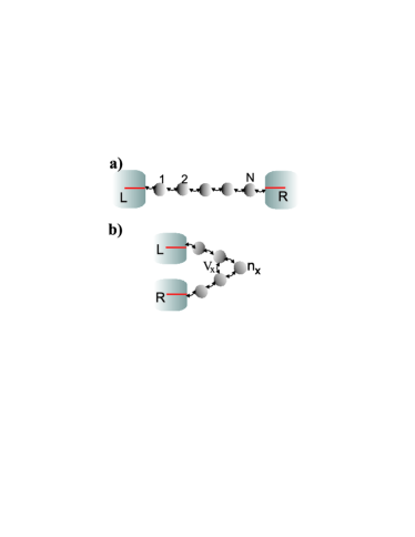
First, let us analyze the position (on the energy scale) of the apex atom energy level, , versus the chemical potential of the STM electrode. For () the tip is not charged (is charged) and for is neutral. In most of our calculations we set the energy level of the apex atom below the Fermi energy of the STM electrode because in this case the STM tip is charged. Here we give the reason of our choice. Using the basic electrodynamic relations one can show that additional charge is gathered on sharp edges and curvatures. To confirm this rule for the STM we consider here a simple model of the STM tip i.e. one-dimensional bend monoatomic wire. In Fig. 1a the schematic view of a straight wire with the nearest neighbor couplings between atoms, , is shown. For a bend wire, Fig. 1b, also the next neighbor hopping has to be considered, . The Hamiltonian for this system is given by
| (1) | |||||
where stands for the middle atom in our wire, , is odd. The main quantity of our interest is the occupation of this middle atom, , which represents the last tip atom. The local charge at this atom can be expressed by means of the retarded Green’s function, i.e. . The function can be obtained from the equation of motion for the retarded Green’s function and in our case [for atom wire with the same electron energies, , and within the wide band approximation, ] it becomes:
| (2) |
where , and matrix reads:
| (8) |
The determinant of this matrix can be expressed by means of the Chebyshev polynomials of the second kind, [16], and finally the retarded Green’s function, , can be obtained analytically. It helps us to find the occupation of the middle atom in the wire, as a function of parameter.

In Fig. 2 we show the charge localized at the middle atom versus the coupling parameter for the wire length (solid line) and (broken line). The parameter is responsible for the wire curvature i.e. for the wire is straight and for nonzero we have a kind of bend wire as is depicted in Fig. 1b. Here we consider the case which leads to half occupation of all wire sites for ( is the chemical potential of the electrode). However, for nonzero the occupation of the middle atom increases and e.g. for it is about larger than for the straight wire. This result indicates unquestionably that there is additional electron charge at the middle atom. This atom corresponds to the last tip atom and is more occupied in comparison with other atoms.
Here we should comment on the last result. Of course, STM tips are not fabricated by bending a straight monoatomic wire. However, a sharp STM tip, with only one atom, can be described as a kind of short bend wire e.g. with or atoms. In this case the coupling is responsible for the tip curvature and the larger the sharper tip is (there is physical limit on - it cannot be larger than twice or a few values of parameter). Thus, this approach is suitable for description of sharp tips and failed for rather wide ones. Note, that in the literature STM tips are often much more simplified and modelled by a semi-infinite chain of atoms, e.g. [17, 18] or an ideal fermi gas electrode (energy structure-less).
On the other hand, one can consider the last tip atom as a kind of additional atom (adatom) which is put on metallic STM electrode. This atom cannot be treated in the same way as atoms inside the STM electrode, first of all because its neighborhood is different in comparison with other atoms in the tip. Moreover, the energy of affinity (and ionization) level at the apex atom depends on the distance between this atom and the STM metallic surface. This effect is known in chemisorption processes, i.e. the affinity energy level decreases its value versus the surface Fermi energy with the distance adatom-surface and is minimal for an adatom placed directly on a surface, cf. [19]. In that case electrons from the surface can occupy the adatom affinity state which leads to minimalization of the total energy (cf. also the calculated local DOS of Co atoms at Au surface which is characterized by local peaks under the Fermi level, [20]). This explanation support our idea that the STM tip is charged. Also dynamical polarization effects (surface-adatom or surface-molecule) can renormalize molecular states, [21].
Taking into account the above considerations we assume in our calculation that the energy of the last tip atom, , lays slightly below the STM chemical potential, i.e. , and thus is more occupied. One can obtain the same effect for but the STM tip should be considered as a bend wire, cf. Fig. 1b. In the last case the middle atom in the wire is extra occupied (its density of states possesses a local maximum below the Fermi energy). It allows us to treat the STM tip as a metallic electrode with only one atom under the condition .
3 Theoretical STM model
The system consists of the STM tip, an object (few-atom system, i.e. one atom or short wire) and a metallic surface, cf. Fig. 3 for only one atom on the surface. The STM tip can be represented by (i) a metallic electrode i.e. tip 1, Fig. 3a - electrons flow from this electrode directly to the investigated object, (ii) a metallic electrode with the last tip atom on it, i.e. tip 2, Fig. 3b - electrons flow from the electrode through this apex atom then through the object on the surface, and (iii) a metallic electrode with the apex atom but electrons can flow from the STM electrode directly to the object or through the last tip atom - tip 3, Fig. 3c.
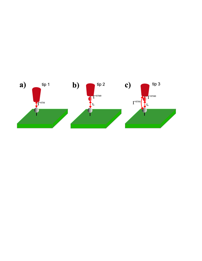
Tip 2 in Fig. 3 is suitable for very sharp STM tips and tip 1 (widely used in the literature) describes rather blunt tips. The third case, tip 3, can be treated as a composition of the first and the second tips. To obtain the current flowing from the STM electrode we use the Green function formalism and thigh-binding Hamiltonian, cf. [11, 14], which can be written as follows:
| (9) |
where describes electrons in the STM tip. For a metallic STM electrode it can be expressed in the form (ideal Fermi gas): , which corresponds to Fig. 3a or with one tip atom, cf. Fig. 3b,c:
| (10) |
Here and represent electron energies in the STM electrode and at the tip atom. and are the creation and annihilation electron operators in an appropriate electron state and stands for the coupling parameter between the STM electrode and the tip atom ( in Fig. 3 depends on this parameter). The surface, similarly to the STM electrode, is modelled as an ideal Fermi gas by the Hamiltonian, . The object Hamiltonian depends on the number of atoms at the surface and e.g. for a single atom it can be written as , but for a short wire it has the following form
| (11) |
The coupling Hamiltonian is responsible for electron tunnelling between the STM and the surface electrode and for , Eq. 10, and , (tip 2, Fig. 3b) it can be expressed as: , where is the hopping integral between the tip atom and the object atom. Note, that for -site wire on the surface one should change the coupling Hamiltonian and instead of operator one has to sum operators over all atomic sites in the wire i.e. . Moreover, for the system shown in Fig. 3c one has to add to the Hamiltonian the term which is responsible for the coupling between the STM electrode and the object atom. Thus the coupling Hamiltonian becomes:
| (12) |
where we assume that the STM electrode is connected with the first atom in the wire via element (it is responsible for parameter, cf. Fig. 3c). The role of electron-electron interactions in the system is discussed in Sec. 4.2. Electron transport properties are analyzed within the framework of the Green’s function method. The tunnelling current flowing from the STM electrode to the surface can be obtained from, [22]:
| (13) |
where is the Fermi function and the external voltage is expressed by means of the STM and surface chemical potentials i.e. . The transmission function for considered here systems reads:
| (14) |
where is the matrix composed of the coupling parameters between the STM electrode or the surface with the object atoms. In general the elements of these matrixes can be written in the form , and similar for . The next matrixes in Eq. 14 are composed of the retarded and advanced Green functions (), and can be obtained from the equation of motion for the retarded Green’s function. Note, that for our systems, Fig. 3, the transmittance can be obtained analytically and all matrix elements will be specified later. The knowledge of the current flowing through the system and the STM voltage is sufficient to find the differential conductance, , or the normalized differential conductance, .
4 Results and discussion
In this section we show and analyze the current and differential conductance as a function of the surface chemical potential (). It is worth noting that all object atoms are placed directly on the surface and thus we assume that their onsite energies are shifted with the surface chemical potential, . The same is true for the last tip atom and the STM electrode. This procedure is justify in our system as the largest potential drop is observed for the weakest coupling - in our case this is parameter which is at least times smaller than the other couplings (the tip and the substrate are in local equilibrium). All results in this section are obtained for the energy unit . The current and conductance are expressed in the units of and , respectively, and e.g. for eV the current unit corresponds to A. The other parameters have been chosen in order to satisfy the realistic situation in many STM experiments, e.g. [11, 13, 15].
Note that in our calculations we chose fully symmetrical objects in the energy space. The first object is a single atom on a surface which is characterized by the Lorentz-type density of states (DOS). The second one stands for a short wire also with symmetrical DOS. It is obvious that in real situation such atomic objects on a surface can be characterized by asymmetrical DOS e.g. due to different couplings object-surface. In that case the differential conductance curves have to be also asymmetrical and it is difficult to analyze the role of charged tip in this asymmetry. To avoid this problem we concentrate here on objects with symmetrical DOS.
4.1 STM tunnelling through a single atom
For a single atom on the surface the following analytical solutions for and matrixes can be obtained:
-
1.
Tip 1, Fig. 3a: , and , where , are energy independent (wide band limit approximation). According to the above relations the transmittance becomes:
(15) -
2.
Tip 2, Fig. 3b (there are two atoms and we assume that the index 1/2 in all matrixes corresponds to the object/STM tip atom) nonzero matrix elements are: , , and the transmittance is expressed as follows: , where
(16) -
3.
Tip 3, Fig. 3c, nonzero matrix elements are: , and thus the transmittance becomes:
(17) where
(18) (19)
The knowledge of the transmittance allows us to find the current flowing in the system and the differential conductance.

In order to reveal the role of charged tip we investigate the STM current for all described tip models. In Fig. 4 the current-voltage characteristics are shown for the case of the neutral tip (upper panel) and the occupied one (lower panel). The broken lines are obtained for the simplest model where the STM tip is represented by a metallic electrode without any tip atom, cf. Fig. 3a. Thus the broken line is independent on parameter and is the same in both panels. The current in this case is monotonic function of the voltage. The thin solid (thick solid) lines correspond to tip 2, Fig. 3b (tip 3, Fig. 3c). The currents obtained within both tip 1 and tip 3 are very similar because the object atom for these cases is coupled directly with the STM electrode, cf. the broken and thick lines. In contrast to this, the current is not monotonic function for tip 2 and takes nonzero values only for , cf. thin solid lines, both panels. In the last case electrons can tunnel from the STM electrode to the surface only though the tip atom and the object atom. This is the reason why the current flows if there are nonzero local density of states at both atoms in the window of the chemical potentials. This effect is also reflected in the current curve obtained for tip 3 model for (thick line, lower panel). In this case the current is characterized by a local minimum for . The current-voltage characteristics obtained for the neutral and occupied tip atom seem to be similar to each other, cf. the upper and the lower panel for the broken, thick or thin lines, respectively. However, there are very important and crucial for our paper differences which become prominent on the differential conductance curves.

In Fig. 5 we show the differential conductance obtained for the corresponding current curves from Fig. 4. Note that the conductance curves obtained according to tip 1 are the same at both panels (cf. broken lines) and reflect the local density od states of the object atom. As a most prominent feature, the conductance turns out to be symmetrical versus for the case of neutral STM tip (upper panel) and asymmetrical for charged tip atom (lower panel). The explanation of this fact is as follows, i.e. for the neutral tip the probability of electron tunnelling from the surface to the STM tip or vice versa is the same (the absolute currents for positive and negative voltages are the same, cf. Fig. 4, upper panel). If the tip is charged these probabilities are not equal and for electrons it is easier to tunnel from the tip to the surface states than from the surface to the STM electrode.
It is interesting that in the presence of the tip atom we find the negative differential conductance, cf. thin solid lines in Fig. 5 obtained for tip 2. The negative conductance is related to the discrete structure of the local density of states at both (STM and object) atoms (cf. [15] where the negative conductance was observed for non-constant surface density of states). If the overlap between the tip and the surface states decreases (with increasing chemical potential) the negative differential conductance appears, [23], (see [24] for other explanation of NDC). This condition can be satisfied only for certain range of parameters. For tip 3, thick lines, the negative conductance appears only for the case of charged tip (lower panel) and due to the direct coupling , it is not as prominent as for tip 2 (, thin lines). It is worth to comment on the last result. In real STM experiments it is very difficult to observe the negative conductance mainly due to not very sharp tip, temperature effects or direct coupling between the STM and the surface electrode (not through the object). The last factor gives only constant positive value to the conductance (the corresponding current depends linear only on the chemical potential difference) and shift the conductance curves above the OX axis. Thus in our calculations we omit this coupling and concentrate on the charged tip effects.

The next intriguing question is whether the energy position of the last tip atom, , influences the asymmetry effect. To investigate this problem we chose the third model of the STM system, (viz tip 3, Fig. 3c). In Fig. 6 we show the differential conductance curves obtained for (the neutral tip, broken line), , and , thin solid and thick solid lines, respectively. For (charged tip) we observe, as before, asymmetrical conductance curves versus the zero voltage. Moreover, the more charged is the tip the stronger asymmetry is observed. A common feature of all curves is the emergence of peaks for and , which is visible especially for the thick curve, (the peak for is related to the energy level of the apex STM atom). This effect could be used to test the quality of the STM tip. The apex tip atom leaves its fingerprints in the differential conductance curves: First, the conductance curves are asymmetrical and second, the conductance peak related to the tip atom should appear. Note, that using first-principles calculations, the studies of the geometrical, electronic, and dynamic properties of a single atoms adsorbed on silicon or tungsten surfaces were reported e.g. in Ref. [25, 26].
4.2 STM tunnelling through a single atom - the role of Coulomb interaction
In this subsection we analyze the influence of Coulomb interaction between the STM tip and one-atom object on the electron transport through this system, cf. Fig. 3c. The interaction Hamiltonian can be written in the following form:
| (20) |
Here we restrict our investigation to non-magnetic atoms and do not consider many-body effects like the Kondo effect, charge-spin separation effect and others. It allows us to use a Hartree-Fock like approximation and the interaction can be captured by renormalizing the on-site energy levels. In this case we can substitute by and by where stands for the charge occupation of the atom on a surface and the STM apex atom, respectively. The occupations, , can be obtained from the the knowledge of the retarded Green functions according to the relation , and similar for . In this case it is impossible to derive analytical solutions for the current or the conductance as the retarded Green function depends on both (the surface and the STM) atom occupations and is found numerically in the self-consistent way.

In Fig. 7 the influence of Coulomb interaction on the differential conductance through one-atom object on a surface is studied. The upper (lower) panel corresponds to the neutral, (occupied, ) STM tip. For very week interaction, , the differential conductance curves are very similar to those ones obtained for , cf. the broken and thick solid lines in Fig. 6 with the broken lines in Fig. 7. For stronger Coulomb interaction, there are subtle effects in the differential conductance curves in comparison with the case for . The main conductance peak related to the surface atom state, for , is slightly changed for the neutral STM tip. For the occupied STM tip the position of this peak is shifted towards the negative values of . It results from the renormalization of the on-site atom energy i.e. the STM apex atom is strongly charged which shifts the on-site surface atom energy above the fermi level - this leads to the conductance peak below . The results shown in Fig. 7 confirm that the Coulomb interactions slightly change the differential conductance structure and can be omitted in our studies.
Moreover, the electron-electron Coulomb on-site interactions are also neglected in our system as we consider here non-magnetic atoms (e.g. a tungsten tip, an object made of silver, gold or lead atoms and silicon-gold surface, cf. [11, 13]) and, as was mentioned above, do not study many-body effects.
4.3 STM tunnelling to a short wire
In order to corroborate the results of the previous subsection we have computed the STM differential conductance for a quantum wire on a surface (instead of the single atom considered in Sec.4.1). The wire consists of atoms with the same onsite energies, , and the nearest neighbor couplings, . The coupling wire-surface is described by the function , and is defined as before. The wire is characterized by fully symmetrical local density of states: It is very important in these studies - for asymmetrical DOS the conductance is also asymmetrical. In our calculations we assume that the STM tip is connected with the first wire atom (the results for other connections are similar). The calculated method is the same as in the previous subsection thus here we give only the relations for the transmittance through three considered systems (cf. Fig. 3 but for 3-site wire on the surface):
-
1.
Tip 1, Fig. 3a: .
-
2.
Tip 2, Fig. 3b (there are four atoms and we assume that indexes: 1,2,3 describe the wire sites and index 4 corresponds to the tip atom): .
-
3.
Tip 3, Fig. 3c: .
and the retarded Green functions are obtained from the equation of motion for these functions. Note, that the transmittance for tip 3 is not a simple sum of the transmittance obtained for tip 1 and tip 2 due to parameter which appears directly in the transmittance relation and also in the above Green functions.

Figure 8 depicts the differential conductance obtained for short quantum wire ( atomic sites) for the neutral (, upper panel) and occupied tip atom (, lower panel). Such a wire is characterized by three-peak density of states which is reflected also in the differential conductance curves (cf. the broken line obtained for tip 1, upper panel). The thin solid (thick solid) lines correspond to tip 2 (tip 3) and these peaks are also visible in these cases. For the neutral tip all conductance curves are fully symmetrical (upper panel), cf. also Fig. 5. However, for the occupied tip the conductance curves are asymmetrical versus (lower panel) which is in accordance with the previous results. This asymmetry in the conductance is very well visible for the thin solid line obtained for tip 2 (Fig. 8, lower panel, thin line). Here, for a local conductance peak appears but for there is no such maximum in the differential conductance. The conductance curve obtained for tip 3 (thick line) is also asymmetrical. It is very interesting and important fact that the occupied tip influences all conductance peaks (cf. the thick and thin lines, lower panel) and not only the peak near . For one additional peak appears which is the same effect as observed for the case of , Fig. 5. This peak is very well visible for tip 2 (thin line) but for tip 3 the main conductance peak for compensates the peak for . Moreover, as before, the negative differential conductance is observed for the results obtained for tip 2 and tip 3.

A remaining question is whether the position of influences in the same way all differential conductance peaks. Therefore we plot in Fig. 9 the differential conductance as a function of the surface chemical potential, , and . Here, the symmetry of the conductance for the neutral tip is visible for and asymmetrical shapes of for negative . It is interesting that the occupied tip influences mainly the conductance for negative potentials i.e for . For positive the conductance peak is slightly modified. Moreover, in Fig. 9 the evolution of the additional peak which appears for is visible. For small values of this peak is compensated by the main conductance peaks (which appear for ), cf. also Fig. 8.
Of course, in the STM experiments it is very difficult (or even impossible) to change the tip occupation or parameter. However, it is possible to use different kind of tips (blunt or sharp) or other atoms attached to the tip. In the last case during the measurement of the same object, one should obtain different asymmetries of the conductance as each atom is characterized by different parameter. This experimental procedure, however, can destroy the tip or change its geometry which can also lead to asymmetrical results.
5 Comparison with experiment
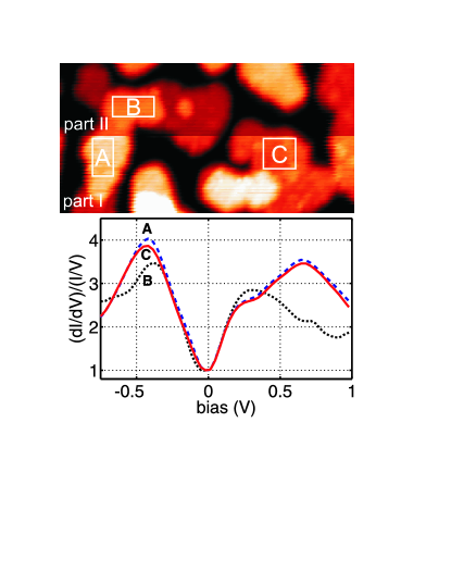
In this subsection we compare our theoretical results with the STM experiment on thin Ag films. Ag was grown on Si(111)-(66)Au substrate held at room temperature in an UHV condition. The vacuum chamber was equipped with a RHEED (Reflection High Electron Energy Diffraction) apparatus and STM (type OMICRON VT). Electrochemically etched and annealed in UHV W tip was used. The base pressure was mbar. The average thin Ag film thickness was equal to 3 ML of Ag(111). This procedure yields flat Ag islands with (111) orientation, as indicated by the RHEED pattern appearance. Figure 10, upper panel, shows a constant-current scanning tunneling microscope image of the sample which was used for current-voltage spectra measurements. The sample was composed of well separated islands with some hexagonal shape. Close inspection of the island’s surface morphology reveals presence of grainy features with diameter of about nm. Consequently, the surface appears rough, independent of the island height. Although RHEED patterns obtained for this sample showed streaky features corresponding epitaxially ordered structure, somewhat diffuse width of the streaks indicated imperfect order. On Ag islands denoted as A, B, and C in Fig. 10, upper panel, were measured current-voltage spectra and calculated the quantity , which is related to the density of states [27, 28]. The thickness of islands determined from the profile lines and counted from the wetting layer surface was equal to 1.05 nm for areas A and B and 0.8 nm for the island C. Figure 10, lower panel, shows the STS spectra measured on Ag islands shown in the upper panel of Fig. 10. Each spectrum in the lower panel is the average of 60-90 individual spectra in order to enhance the signal-to-noise ratio. The experiment reported here is a good example of a phenomenon frequently occurring during STM measurement practice - a sudden variation of the tip length which is a consequence of the tip apex rearrangement. Here the scan begins at the bottom, and in the middle the average level of the image lowers of 1.5Å. Apparently, the tip became shorter. In order to keep the tunneling current constant, the STM scanner approached the sample. It is also visible that the resolution achieved for the lower part is better than for the upper part of the image. Thus the tip switches from ”sharp” configuration (part I) to the ”blunt” one (part II). As the both areas A and B are on the same island, with the same thickness, the electronic structure of the sample side of the tunneling junction is identical. We note that in following experiment on the same sample we observed also reversible variations of the tip length. Figure 10 shows no evidence of touching of the sample and one can assume that in course of the scan the tip has lost the very top element, presumably a single atom.
The variation of the topographic image is in accord with electronic structure changes shown in Fig. 10, lower panel. The curve A, from the area scanned by the sharp tip (part I), is displayed together with the curve B measured on the area B with the blunt tip (part II). As a most prominent feature we observe two quantum states at the surface voltages eV and eV for both tips (curves A and B) and one additional state for eV observed only for the sharp tip (curve A). For comparison we also measured spectra of the island C with the thickness 1 ML smaller than for A and B. It is shown in Fig. 10, lower panel, as curve C. The curves A and C are essentially identical. This fact excludes thickness-related changes of the thin film electronic structure, namely the Quantum Size Effect (QSE) [29], as well as thickness-dependent shift of the Ag surface state binding energy, as observed during photoemission experiment [30]. Although the detailed knowledge of the origin of the states observed in STS spectra is not important for the following discussion, we expect that they are relevant to the grainy structure of the island. Therefore, one of the possible candidates are electronic states of the silver clusters, like the clusters on graphite surface, studied with STS in [31].
To analyze theoretically the experimental results we use the method described in the previous section and consider two STM tips: a metallic electrode, tip 1 (Fig. 3a), and the tip with one apex atom, tip 2 (Fig. 3b). The first one corresponds to the STM-tip from part II of our experiment whereas the second one is responsible for part I (the tip is sharper). Two Ag surface states which are visible in Fig. 10, lower panel, for eV and eV are generated in our model by means of two coupled atomic sites situated on a metallic surface (for our purposes the origin of these states is not important). Fig. 11 depicts the density of states (for two atoms on the surface) for the symmetrical (DOS1) and asymmetrical (DOS2) cases which are used in our calculations.


In Fig. 12 the normalized conductance as a function of the surface voltage is shown for the symmetrical (upper panel) and asymmetrical (lower panel) surface DOS (obtained according to tip 2 model) and for different tip occupation, and - thin solid, solid and thick solid lines, respectively. The case of corresponds to the neutral tip and the results are very similar to the differential conductance curves obtained for the tip without the apex atom i.e. for tip 1, broken lines. Note, that for these cases (metallic tip or the tip with neutral apex atom) the conductance curves are characterized by two maxima which reflect only the surface quantum states. This situation corresponds to the blunt STM tip used in our experiment (part II). The thick solid lines in Fig. 12 correspond to the case of occupied tip, , and the additional peak for eV is visible. (Remark: the STM tip states which are below the Fermi level, on the conductance graphs are visible for positive surface voltage). It is high probably that the origin of this peak is related to the apex atom energy level which is below the Fermi energy and is occupied (the surface states in the experiment are the same for both parts but the tip has changed). The similar effect appears in Fig. 5 or Fig. 6, where for charged tip additional structure in the conductance was observed. Thus, the broken curves in Fig. 12 represent the STM tip from part II and the thick solid lines correspond to the tip from part I. Moreover, for asymmetrical DOS, lower panel, the qualitative comparison of the differential conductance with the experiment is better which suggests that the intensity of Ag surface states (below and above the Fermi level) are different, cf. Fig. 11, DOS2.
It is interesting that the normalized differential conductance peaks are not proportional to the surface DOS and the results obtained for symmetrical and asymmetrical DOS do not reflect strong asymmetry which appears for DOS2, cf. Fig. 11. It means that the intensity of peaks are not directly proportional to the surface DOS (the positions of these peaks are related to the surface or STM DOS), cf. also [27]. Only for nearly constant tip density of states the normalized differential conductance is proportional to the sample DOS, [28]. Thus, using STS results it is difficult to distinguish between the surface and the STM tip states due to their energy convolution. One possible way is to scan two or more different areas of the surface (characterized by different structure or different atoms) - if there are some states which appear for both areas (for the same voltage) there are probably the STM states.
To conclude, the STM states influence the conductance behavior and disturb the intensity of the conductance peaks. For charged STM tip, , it leads to the symmetry braking in the differential conductance, , which is also visible on the normalized differential conductance curves, . It is worth noting that the position of the additional peak on the differential conductance curve, Fig. 12, obtained for eV is in good agreement with the results reported in Ref. [4], Fig. 6, where the authors investigated Au(111) surface by means of the tungsten tip and observed a special peak for eV which, in their opinion, was a halo of the tip structure. In our studies the position of the tip-induced peak is very similar which indicate that in experiments with sharp tungsten tip a local maximum around the sample voltage eV should be observed. This is also consistent with the STS results on Cu(111) surface, [32], where the differential conductance peak for the sample voltage eV appears and is identified as a halo of the tungsten sharp STM tip (fcc pyramid configuration, cf. also [26]).
6 Conclusions
In summary, using the Green’s function technique for the tight-binding Hamiltonian the STM transport properties through surface states have been studied. It was shown that sharp STM tip, represented by a kind of bending wire, is extra occupied. In this case the analytical relation for the Green’s function needed to obtain the local charge has been obtained for arbitrary wire length, , Eq. 2.
The current and the differential conductance have been studied for three models of the STM tip and for two objects on the surface (single atom and short wire). The analytical formulas for the transmittance and the retarded Green functions have been obtained. For the neutral STM tip the conductance has turned out to be symmetrical versus the surface chemical potential, (cf. Fig. 5, upper panel) and asymmetrical for charged tip atom (Fig. 5, lower panel and Fig. 9). Thus for occupied tip all differential conductance curves are asymmetrical, although the density of states of investigated objects are fully symmetrical in the energy space. Additional peak in the conductance has been observed for the STM voltage which corresponds to the onsite energy of the last tip atom. It means that this peak is a feature of the STM tip and thus it should be observed for different objects at the surface.
To confirm our theoretical calculations the STM experiment on Ag islands with two different tips has been carried out. Additional peak in the conductance curve for eV has been observed for sharper tip which is a halo of the tip quantum state. This peak has not been registered for the blunt tip, cf. Fig. 10. Our theoretical calculations obtained for charged STM tip, Fig. 12, are in good agreement with the experimental results. Alternatively, such an experiment may be also performed with metallic molecules or clusters on a surface, e.g. [33, 34]. It has been also shown that the normalized differential conductance peaks are not directly proportional to the surface DOS. Moreover, the results obtained for symmetrical and asymmetrical DOS do not reflect asymmetry in the peak intensity of the surface DOS.
Acknowledgements. This work has been supported by Grant No N N202 1468 33 of the Polish Ministry of Science and Higher Education.
Bibliography
References
- [1] G. Binning, H. Rohrer, Ch. Gerber, and E. Weibel, Phys. Rev. Lett. 49, 57 (1982).
- [2] J.P. Pelz, Phys. Rev. B 43, 6746 (1991).
- [3] W.A. Hofer and J. Redinger, Surf. Sci. 447, 51 (2000).
- [4] M. Passoni, F. Donati, A. Li Bassi, C. S. Casari, and C. E. Bottani, Phys. Rev. B 79, 045404 (2009).
- [5] W.A. Hofer and A. Garcia-Lekue, Phys. Rev. B 71, 085401 (2005).
- [6] J. Tersoff and D.R. Hamann, Phys. Rev. B 31, 805 (1985).
- [7] N. Li, M. Zinke-Allmang, and H. Iwasaki, Surf. Sci. 554, 253 (2004).
- [8] S. Loth, M. Wenderoth, L. Winking, R. G. Ulbrich, S. Malzer, and G. H. Dohler, Phys. Rev. Lett. 96, 066403 (2006).
- [9] H. Narita, A. Kimura, M. Taniguchi, M. Nakatake, T. Xie, S. Qiao, H. Namatame, S. Yang, L. Zhang, and E. G. Wang , Phys. Rev. B 78, 115309 (2008).
- [10] R. Dombrowski, Chr. Steinebach, Chr. Wittneven, M. Morgenstern, and R. Wiesendanger, Phys. Rev. B 59, 8043 (1999).
- [11] M. Krawiec, T. Kwapiński, and M. Jałochowski, Phys. Rev. B 73, 075415 (2006).
- [12] D. Tomanek, S.G. Louie, H. Jonathon Mamin, D.W. Abraham, R.E. Thomson, E. Ganz, and J. Clarke, Phys. Rev. B 35, 7790 (1987).
- [13] M. Krawiec, T. Kwapiński, and M. Jałochowski, Phys. Stat. Sol. B, 242 ,332 (2005).
- [14] W.A. Hofer, A.S. Foster, and A.L. Shluger, Rev.Mod.Phys. 75, 1287 (2003).
- [15] M. Krawiec, M. Jałochowski, and M. Kisiel, Surf.Sci. 600 ,1641 (2006).
- [16] T. Kwapiński, J.Phys.: Condens. Matter 18, 7313 (2006).
- [17] H. Ou-Yang, B. Kallebring, and R.A. Marcus, J. Chem. Phys. 98, 7565 (1993).
- [18] B.A. McKinnon, T.C. Choy, Phys. Rev. B 54, 11777 (1996).
- [19] M.-C. Desjonqueres and D. Spanjaard, Concepts in Surface Physics (Springer, Berlin 1996).
- [20] O. Ujsaghy, J. Kroha, L. Szunyogh, and A. Zawadowski, Phys. Rev. Lett. 85, 2557 (2000).
- [21] K.S. Thygesen and A. Rubio, Phys. Rev. Lett. 102, 046802 (2009).
- [22] Y. Meir and N.S. Wingreen, Phys. Rev. Lett. 68, 2512 (1992).
- [23] Y. Xue, S. Datta, S. Hong, R. Reifenberger, J.I. Henderson and C.P. Kubiak, Phys. Rev. B 59, R7852 (1999).
- [24] M.K.-J. Johansson, S.M. Gray, and L.S.O. Johansson, Phys. Rev. B 53, 1362 (1996).
- [25] G. Chen, Xudong Xiao, Y. Kawazoe, X. G. Gong, and C. T. Chan, Phys. Rev. B 79, 115301 (2009).
- [26] W.A. Hofer, J. Redinger, and P. Varga, Solid State Commun. 113, 245 (2000).
- [27] M. Passoni, and C. E. Bottani, Phys. Rev. B 76, 115404 (2007).
- [28] R.M. Feenstra, J.A. Stroscio, and A.P. Fein, Surf. Sci. 181, 295, (1986).
- [29] A. L. Wachs, A. P. Shapiro, T. C. Hsieh, and T.-C. Chiang, Phys. Rev. 33, 1460 (1986); T.-C. Chiang, Surf. Sci. Rep. 39, 181 (2000).
- [30] F. Patthey, W. -D. Schneider, Surf. Sci. Lett. 334, L715 (1995).
- [31] H. Hövel, B. Grimm, M. Bödecker, K. Fieger, B. Reihl, Surf. Sci. 334, L603 (2000).
- [32] A.L. Vazquez de Praga, O. S. Hernan, R. Miranda, A. Levy Yeyati, N. Mingo, A. Mart n-Rodero, and F. Flores, Phys. Rev. Lett. 80, 357 (1998).
- [33] S. P. Gubin, V. V. Kislov, V. V. Kolesov, E. S. Soldatov, and A. S. Trifonov, Nanostructured Materials 12, 1131 (1999).
- [34] S. Voss, M. Fonin, U. Rüdiger, M. Burgert, and U. Groth, Appl. Phys. Lett. 90, 133104 (2007).