Power-dependent internal loss in Josephson bifurcation amplifiers
Abstract
We have studied nonlinear superconducting resonators: coplanar-waveguide (CPW) resonators with Josephson junctions (JJs) placed in the middle and CPW resonators terminated by JJs, which can be used for the qubit readout as “bifurcation amplifiers.” The nonlinearity of the resonators arises from the Josephson junctions, and because of the nonlinearity, the resonators with appropriate parameters are expected to show a hysteretic response to the frequency sweep, or “bifurcation,” when they are driven with a sufficiently large power. We designed and fabricated resonators whose resonant frequencies were around 10 GHz. We characterized the resonators at low temperatures, K, and confirmed that they indeed exhibited hysteresis. The sizes of the hysteresis, however, are sometimes considerably smaller than the predictions based on the loaded quality factor in the weak drive regime. When the discrepancy appears, it is mostly explained by taking into account the internal loss, which often increases in our resonators with increasing drive power in the relevant power range. As a possible origin of the power-dependent loss, the quasiparticle channel of conductance of the JJs is discussed.
pacs:
84.40.-x, 74.50.+r, 85.25.CpPhys. Rev. B 80, 174502 (2009) [DOI: 10.1103/PhysRevB.80.174502]
I Introduction
In many experiments related to quantum information processing, the readout plays a critical role. One of the recent major steps forward in the experiments of superconducting qubits was related to the improvement of readout, and the quantum nondemolition readout was reported.Wallraff et al. (2005) In the readout scheme of Ref. Wallraff et al., 2005, the charge qubit was non-resonantly coupled to a superconducting linear resonator. The qubit state was detected as a shift in the resonant frequency of the resonator. The measurements were done with a weak driving power of , where is the number of measurement photons populated in the resonator.
It has been suggested that employing a nonlinear resonator instead of linear resonator should relax the strong demand of low-noise broadband microwave measurements because the latching effect between the bistable states in a nonlinear resonator is expected to provide a larger but still fast enough response.Siddiqi et al. (2004) Such scheme, or the “bifurcation amplifier,” has been applied to the readout of charge qubitsSiddiqi et al. (2006); Boulant et al. (2007); Metcalfe et al. (2007) and flux qubits,Lupaşcu et al. (2004, 2006); Lee et al. (2007); Lupaşcu et al. (2007) where Josephson junctions (JJs) as nonlinear inductors are employed for the nonlinear resonators. In many cases, the nonlinear resonators with JJs have lumped-element capacitors, and their resonant frequencies are around 1 GHz.Lupaşcu et al. (2004); Siddiqi et al. (2006); Boulant et al. (2007); Lee et al. (2007); Lupaşcu et al. (2007) In general, however, using a distributed element such as a coplanar waveguide (CPW)Metcalfe et al. (2007); Boaknin et al. (2007); Naaman et al. (2008); Inomata et al. (2009) makes it easier to increase the resonant frequency and the quality factor. A higher resonant frequency is advantageous for suppressing photon-number fluctuations, which may cause qubit dephasing even when the readout circuit is turned off.Bertet et al. (2005) Choosing a high quality factor and a resonant frequency much higher than the qubit frequency would be also helpful in suppressing the qubit relaxation through the resonator.Houck et al. (2008)
In this work, we have characterized at low temperatures, K, nonlinear CPW resonators with JJs, whose resonant frequencies are as high as GHz. We observed the “bifurcation” as expected theoretically; the resonators showed a hysteretic response to the frequency sweep when they were driven with a sufficiently large power. We analyze the hysteresis in detail, paying close attention to the internal loss, which has not necessarily been examined well in the earlier worksLee et al. (2007); Boaknin et al. (2007) on superconducting nonlinear resonators designed for reading out flux and charge qubits.
II Theory
The nonlinear resonators studied in this work are shown schematically in Figs. 1(a) and 1(b). They are and CPW resonators, respectively. The crosses in the figures denote either single JJs or dc SQUIDs, the origin of the nonlinearity. We treat dc SQUIDs as single JJs with tunable critical currents . Here, we should mention that superconducting transmission lines can also exhibit nonlinearity.Chin et al. (1992); Ma et al. (1997); Tholén et al. (2007) The microwave power required for this effect, however, is many orders of magnitude larger than the power range of our experiments. Thus, we treat superconducting CPWs as linear elements. Port 1 in Figs. 1(a) and 1(b) is connected to a microwave source, whose equivalent circuits are Figs. 1(c) and 1(d). For uniformity, we always use Fig. 1(c) in this paper. The resonator in Fig. 1(a) has been mappedBoaknin et al. (2007); Naaman et al. (2008) to a series circuit of and JJ [see Fig. 1(e)] in the vicinity of the resonance, by considering the electromagnetic environment seen from the JJ in the linear regime, where the drive is so weak that the resonator does not manifest nonlinearity. The series circuit is one of the nonlinear systems studied by Manucharyan et al.Manucharyan et al. (2007) They solved the equation for the Duffing oscillator by retaining the terms with the first harmonic only, then, mapped several nonlinear systems to the Duffing oscillator by comparing the differential equations of the systems with the Duffing equation.Manucharyan et al. (2007)
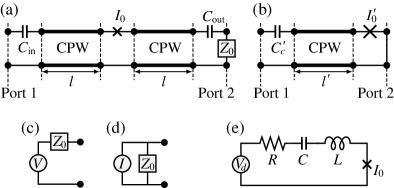
The series resonant circuit in Fig. 1(e) “bifurcates” and becomes bistable in a certain frequency range when the drive amplitude exceeds a critical value , provided that the amplitude of the current through JJ at is sufficiently smaller than . According to Ref. Manucharyan et al., 2007,
| (1) |
and
| (2) |
where
| (3) |
is the loaded quality factor, is the external quality factor, is the unloaded quality factor,
| (4) |
is the Josephson inductance, , satisfies
| (5) |
and is the resonant angular frequency in the linear regime. Equations (2) and (4) suggest that a large and a small are favorable for the bifurcation. When , the normalized boundaries of the bistable region are expressed as
| (6) |
where and is the angular frequency.Manucharyan et al. (2007)
The mappingBoaknin et al. (2007); Naaman et al. (2008) of Fig. 1(a) to Fig. 1(e) has been done for circuits with by assuming that
| (7) |
where and is the coupling capacitance to the input microwave line, and that
| (8) |
Note that the mapping is based on the behavior in the linear regime. We have simulated the circuit in Fig. 1(a) taking into account the drive-strength dependence, as we will describe in the next paragraphs, and confirmed that the simulated and the value calculated from Eqs. (1), (7), and (8) agree reasonably well.
The heart of our simulation is expressing JJ as an inductance that depends on the amplitude of the superconducting-phase oscillation,
| (9) |
where is the Bessel function of the first kind. The idea is based on the following considerations: suppose that the superconducting phase of JJ is oscillating as
| (10) |
Then, the voltage across the junction and the current through the junction are given by
| (11) |
and
| (12) | |||||
Here, let us retain the terms with the first harmonic only, as Manucharyan et al.Manucharyan et al. (2007) did for solving the Duffing equation. Then, Eq. (12) reduces to
| (13) |
By comparing Eqs. (11) and (13) with the equations for a usual inductor , when , we obtain Eq. (9). Note that is nonlinear in the sense that it depends on . Its impedance , on the other hand, is written as
| (14) |
as if it were a usual linear inductor because we retained the terms with the first harmonic only.
Equations (9) and (14) make the simulation easy. Now, for example, it is straightforward to include in the calculations, if necessary, the junction capacitance and the quasiparticle resistance , both of which are parallel to . The relationship between and the quality factors will be discussed in Sec. V. We used the transmission () matrix (see, for example, Sec. 5.5 of Ref. Pozar, 1990) for the simulation. The matrix for an impedance is
| (15) |
and that for a section of lossless CPW with a length is
| (16) |
where is the imaginary unit, is the characteristic impedance, , and is the phase velocity. When CPW has a loss, in Eq. (16) is replaced by , where characterizes the loss.
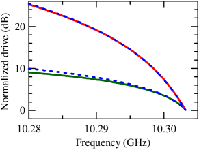
An example of the simulation is shown in Fig. 2. It is for a resonator of the Fig. 1(a) type. The parameters are A, mm, and fF. Both CPWs are lossless with and , where is the speed of light. When we neglected and assumed that , the simulation yielded GHz, , and V. This simulated and the value calculated from Eqs. (1), (7), and (8) agree within 2%. In Fig. 2, the solid curves are the simulated boundaries of the bistable region, and compared with Eq. (6), the broken curves. The vertical axis of Fig. 2 is the drive voltage amplitude normalized by . In general, the solid and broken curves are similar. As the drive amplitude is increased, the difference becomes visible especially for the lower boundary, but this trend should be reasonable because the mapping of Eqs. (7) and (8) is based on the behavior in the linear regime as we mentioned earlier, and because at a given frequency, at the lower boundary is actually larger than at the upper boundary as we will see in Fig. 3(a).
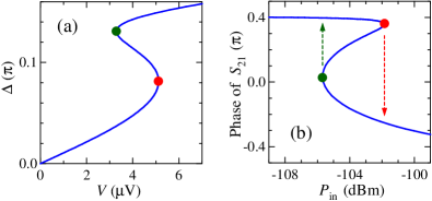
The simulated boundaries in Fig. 2 were obtained by calculating vs. at different frequencies. Such calculation for GHz is shown in Fig. 3(a); the marked local maximum and minimum of are the boundaries. In experiments, we measure instead of , the transmission coefficient of resonators and the reflection coefficient of resonators. These quantities are also simulated by the same method. The phase of is computed in Fig. 3(b) as a function of the incident power , which is more relevant than from the experimental point of view. The power is given by
| (17) |
where
| (18) |
is the amplitude of the incident voltage. Because the section between the markers is unstable, the resonator response in actual measurements is expected to be hysteretic, that is, switching indicated by the arrows in Fig. 3(b) should be observed.
Regarding resonators, when we chose in Fig. 1(b), , , , and the same unit-length CPW properties, the simulation yielded essentially the same etc. as those of the resonator in Figs. 2 and 3.
When we compare the theoretical predictions in this section with experimental results, we should note that in experiments, we cannot make the drive amplitude arbitrarily large in order to see the bistability arising from the nonlinear inductance of JJs because for example, has to be smaller than . Let us also recall that both Eq. (6) and the simulation are based on the approximation of retaining the terms with the first harmonic only; the accuracy of the approximation becomes worse as the drive amplitude increases.
III Experiment
We studied two series of CPW resonators listed in Table 1. The fabrication of Series A, which has single JJs, was almost the same as that of the sample in Ref. Inomata et al., 2009; a Si wafer covered by a layer of thermally oxidized SiO2 was used, Nb interdigital coupling capacitors and Nb CPWs were patterned by photolithography and reactive ion etching, and Al JJs by electron-beam lithography and shadow evaporation. In order to realize a superconducting contact between Nb and Al, the surface of Nb was cleaned by Ar+ milling before the Al evaporation. In Series B with dc SQUIDs, on the other hand, all electrodes including those of SQUIDs are Nb, and everything was fabricated by the photolithographic technology. Thus, between the two series of resonators, there are a couple of differences regarding the CPW that we should note: the thickness of Nb film and the quality of SiO2.
| Reso- | ||||
|---|---|---|---|---|
| nator | Type | (GHz) | (103) | (dBm) |
| A1 | 9.86 | 6 | 97 2 | |
| A2 | 9.70 | 3 | 100 1 | |
| A3 | 9.98 | 1.1 | 101 2 | |
| A4 | 9.83 | 1.6 | 103 3 | |
| B1 | 11.30 | 1.0 | 85 1 | |
| B2 | 11.12 | 1.3 | 82 1 |
The Nb film is much thinner in Series A (0.05 m) than in Series B (0.4 m). As a result, highly likely due to the kinetic inductance,Meservey and Tedrow (1969) we saw a noticeable difference in . In Series A, Nb is deposited directly on the thermally oxidized SiO2 of the Si wafer, whereas in Series B, there is a layer of sputtered SiO2 between Nb and thermally oxidized SiO2. It seems that this sputtered SiO2 decreases . According to Ref. O’Connell et al., 2008, the loss tangent of SiO2 grown by plasma-enhanced chemical vapor deposition (PECVD) is much larger than that of thermally oxidized SiO Thus, it is highly likely that sputtered SiO2 is also much more lossy than thermally oxidized SiO We will come back to this point in Sec. IV.2.
Our resonators (A1, A3, and B1) are designed to be symmetric, that is, in Fig. 1(a), and the two CPWs are the same. For all resonators, we intended to obtain GHz and on the order of with mm, by aiming at , A, , , and fF.
The resonators were characterized in a 3He-4He dilution refrigerator at the base temperature, K. For the characterization, we used a vector network analyzer choosing an intermediate frequency (IF) between 100 Hz and 40 kHz. The transmission coefficient of resonators were measured by connecting Ports 1 and 2 in Fig. 1(a) to the network analyzer. In the input microwave line connected to Port 1, 20-dB attenuators were inserted at K and at the base temperature. The output line had an isolator at K, and at K, an cryogenic amplifier, whose gain at 10–11 GHz was 34–38 dB or 40 dB. For measuring the reflection coefficient of resonators, we employed a directional coupler and extra isolators at the base temperature as in Fig. 1(a) of Ref. Inomata et al., 2009. Magnetic fields were applied in the direction perpendicular to the substrate by means of a superconducting solenoid.
The gains of amplifiers and the insertion losses of attenuators and cables had been characterized at relevant frequencies by independent measurements. The uncertainties of , , and in this paper are less than 1–2 dB.
IV Results
Basic parameters of the resonators are listed in Table 1. We obtained GHz and on the order of as we designed. Hystereses were observed in all resonators; the critical incident power in Table 1 was determined experimentally. The values of for Series A correspond to , A, or the critical current density kA/cm2, within the theoryManucharyan et al. (2007) and the mappingBoaknin et al. (2007); Naaman et al. (2008) in Sec. II. The estimated critical current is on the right order of magnitude, and consistent with the dc measurements on test junctions fabricated on the same wafer, kA/cm2. We also estimated the critical current by the simulation in Sec. II taking into account the junction capacitance, and confirmed that the estimates did not change significantly. The situation is similar in Series B. The estimated kA/cm2 is on the right order of magnitude, and consistent with the parameters of the fabrication process, which targeted at kA/cm2. Below, we focus on Resonators A1 and B1 because within each series, the results were qualitatively similar.
IV.1 Resonator with a single Josephson junction
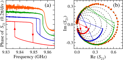
The dependence of Resonator A1 is shown in Fig. 4. At different values of , the frequency was swept up and down while was recorded. At dBm that is, in the linear regime, the phase of vs. shows a usual rotation [the top right curve in Fig. 4(a)], and the polar plot of Im vs. Re falls on the largest dotted circle in Fig. 4(b). The center of the circle is at (, 0), where is the diameter. Note that is equal to the maximum It is also related to the quality factors by
| (19) |
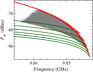
Thus, for Resonator A1 in the linear regime. The other curves in Fig. 4 are for and hysteresis is seen as the theory predicts. An interesting feature in Fig. 4(b) is that the three curves for do not always stay on the largest circle. They move towards smaller circles as increases, and the trend is stronger at larger This dependent quality factors are a key to understand Fig. 5, where the measured bistable region in grey is compared with Eq. (6).
The grey area in Fig. 5 is determined from many two-directional frequency sweeps like Fig. 4(a). If the phase difference of between up and down frequency sweeps at ( ) was more than ( ) in Fig. 5 is grey. The pairs of curves in Fig. 5 are Eq. (6) with different values of The pair with the largest is for in the linear regime and associated with the largest circle in Fig. 4(b). The other pairs in Fig. 5 correspond to the smaller circles in Fig. 4(b) when we neglect the dependence of , which is expected to be much smaller than that of in Resonator A1. The ratio of in Fig. 5 is consistent with Eqs. (1) and (5), that is, the ratio is equal to We treated as an adjustable parameter, and chose its value so that the experimental bistable region stayed between the theoretical boundaries.
The theoretical size of the bistable region in Fig. 5 shrinks rapidly with decreasing , and as we have seen, Fig. 4(b) suggests that of the resonator decreases with increasing especially around the lower boundary, where takes the maximum value. Thus, dependent should mostly explain the fact that the experimental bistable region is considerably smaller than the theoretical prediction for In general, the size of experimentally determined bistable region may depend on the sweep speed due to finite lifetimes of the bistable states. This effect, however, seems to be not significant in Fig. 5 judging from the experiment described in the following paragraphs.
We swept instead of in two directions with kHz, which is much faster than Hz in Fig. 5. We chose GHz and 9.853 GHz, where the widths of the bistable region in Fig. 5 are 8.1 dB and 5.2 dB, respectively. At both frequencies, the values of at which the phase of switched [see also the arrows in Fig. 3(b)] agreed with Fig. 5 within 0.1 dB, despite the large difference in the sweep speed. This is the main reason why we presume that the dependence on the sweep speed is insignificant in Fig. 5.
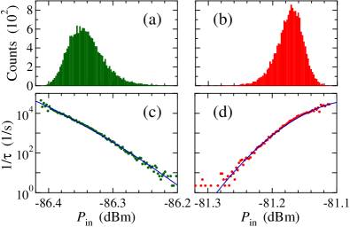
At GHz, the measurements were repeated times, and the histograms of the switching events are shown in Figs. 6(a) and 6(b). The distribution widths of the switching events are much smaller than the width of the bistable region. The histograms can be converted to the lifetimes of the bistable states by assuming that the probability of remaining in the same state decays as , where is the time and in our case, equal to the inverse of IF. This type of conversion has been done many times for the conventional switching from the zero-voltage state to the voltage state in JJs, and the details of the conversion are found, for example, in Ref. Fulton and Dunkleberger, 1974. The lifetimes obtained from Figs. 6(a) and 6(b) are shown in Figs. 6(c) and 6(d), respectively. Below, we analyze within a simple model.
Let us suppose that
| (20) |
and that as in Ref. Kautz, 1988, is associated with the noise. When we further assume for simplicity that is proportional to the minimum where is the noise voltage satisfying , is the source voltage, is the phase noise, and corresponds to one of the theoretical boundaries of the bistable region [see the markers in Fig. 3(a)], the power dependence of is written as
| (21) |
because and are in phase when takes the minimum value. Intuitively speaking, the switching between the bistable states would occur at if an experiment with no noise were possible. The last assumption is actually consistent with the approach based on the Poincaré section in Fig. 2 of Ref. Siddiqi et al., 2004 because the height of the saddle point in the Poincaré section is proportional to the minimum .
The curves in Figs. 6(c) and 6(d) are the least-squares fittings of Eqs. (20) and (21). The fittings yielded dB and dB. Because extends the bistable region by 0.6 dB only in total, the above analysis of at GHz supports our presumption that the dependence on the sweep speed is insignificant in Fig. 5.
IV.2 Resonator with a dc SQUID
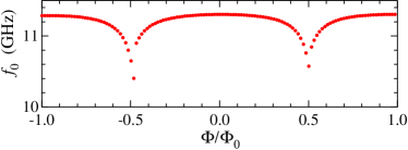
The SQUID modulation of Resonator B1 in the linear regime measured at dBm is shown in Fig. 7. The external dc magnetic flux indeed changes , and thereby, and , periodically. Around the response was a little hysteretic and depended on the direction of the flux sweep. In Fig. 7, the flux was swept in one direction only, and that is why there is small asymmetry at From the amplitude of the modulation, we estimate based on the simulation in Sec. II that at the critical current of the SQUID becomes about 15% of its maximum value, and thus, the SQUID has a normalized loop inductance of where is the critical current per junction at The above value of is consistent with the design.
For different values of we measured the bistable regions. Some of the results are shown in Fig. 8. The rightmost data set was obtained when was close to its maximum value. Regarding quality factors, we found two major differences compared to Resonator A1. One is that in the linear regime is much larger. This should be due to the layer of sputtered SiO2 that exists only in Series B as we mentioned in Sec. III. The other difference is that judging from polar plots (data not shown) like Fig. 4(b), does not change very much when is increased from . Actually, we estimate at , a larger value of than that in the linear regime. The two curves for the rightmost data set in Fig. 8 are Eq. (6) calculated with . They reproduce the experimental boundaries of the bistable region.
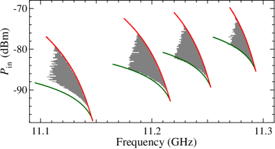
The other data sets in Fig. 8 for smaller values of are also compared with Eq. (6), where we employed for , the estimated values at again. The dependence of on qualitatively agrees with Eq. (1) because a smaller means a larger . As is decreased, however, it becomes easier to see some discrepancies between the experimental boundaries and Eq. (6). In the leftmost data set, for example, polar plots (data not shown) like Fig. 4(b) suggest a moderate decrease of with increasing above . Qualitatively speaking, the behavior of is becoming similar to that in Resonator A1.
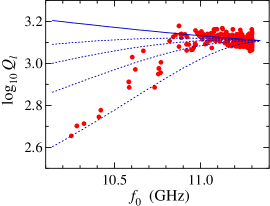
When is decreased further down to GHz, we did not find the bistable region at all, which is a bit surprising because according to Eq. (2), a larger is more advantageous for observing the bistability, in principle. We should not forget, however, that in Eq. (2) depends on as well, and in fact, at GHz decreases with decreasing rather sharply even in the linear regime as shown in Fig. 9, where the vertical axis is the logarithm of and was calculated from the data at dBm. We will discuss the origin of the change in later in the next section. The lifetimes of the bistable states may be also related to the disappearance of the bistable region at GHz. As is decreased, the relevant power range becomes smaller. Within the simple model of Eqs. (20) and (21), smaller and make smaller, and thereby, shorter. Thus, we cannot exclude the possibility that our measurements were not fast enough for observing the bistability at GHz.
V Discussion
In the preceding section, we have seen that how the quality factor depends on or is relevant to the experimental bistable region. In this section, let us discuss the origin of the dependence.
Experimental determination of all the quality factors in Eq. (3) is straightforward in the linear regime. For resonators, is obtained from vs. , and from Eq. (19) by substituting the maximum value of for In Fig. 9, for example, the sharp decrease of at GHz is mostly due to the change in . We have also confirmed that the frequency dependence of is consistent with the theoretical prediction that is determined mainly by . The unloaded quality factor is a measure of the internal loss. In our resonators, both CPWs and JJs can be the source of loss. Resonators A1 and B1 have completely different in the linear regime: and , respectively. As the most probable reason, we have already mentioned the difference in the quality of the dielectric for the CPWs. The value of for Resonators A1 is actually still considerably smaller than those we obtained for usual CPW resonators without JJ fabricated at the same time as Resonators A1. Thus, there should be a contribution from JJ as well.
In the bistable region, it is still possible to estimate the quality factors. We have seen that Fig. 4(b) suggests a strong dependence of in Resonator A1. The dependence is likely to be due to a finite of JJ. The main reason is that the usual CPW resonators without JJ looked almost independent in the relevant power range. In general, of CPW resonators is known to increase with increasing at least in the weak-power range, where the average energy stored in the resonator at is comparable to or smaller.O’Connell et al. (2008) This behavior was also observed in our resonators in the linear regime. Both in Resonators A1 and B1, gained several percents when was increased by 5 dB from dBm. Figure 4(b) is explained if is a function of and its value decreases with increasing , which is quite likely (see, for example, Sec. 6.3 of Ref. Tinkham, 1996). Although we are interested in the case that the JJ stays in the superconducting branch with zero dc voltage, it does not necessarily mean that the ac voltage is also zero. The ac voltage is given by Eq. (11), and when it is nonzero, an ac current flows through causing a loss. This picture is supported by the following quantitative consideration: according to the simulation in Sec. II, the reduction of becomes considerable when is decreased below in Resonator A1, whereas the dc measurements on the test junctions suggest that in Resonator A1 can be as low as . It is also consistent with the results on Resonator B1. Because B1 has a smaller and a much larger superconducting gap, the tunnel barrier of the junctions is thicker. Thus, must be much larger, which explains the fact that dependence is much smaller. The dependence is also explained because modulates the ratio of As approaches increases, but there is no obvious mechanism that changes . We have also confirmed by the simulation in Sec. II that indeed depends on the ratio of and that the experimental vs. in Fig. 9 is qualitatively reproduced with on the order of In Fig. 9, the predictions based on the simulation for different values of are also shown by the solid and dotted curves.
From the viewpoint of the qubit readout and the qubit coherence time, the dissipation due to the loss at can be unfavorable depending on the circuit configuration, and worse than that at CPWs when is closer to the qubit. Fortunately, now we know from the experiment in Sec. IV, how large has to be in order for the loss at to be negligible. For our resonators in Table 1, the ratio of needs to be larger than according to the simulation in Sec. II. This condition should be easily satisfied even with Al JJs by employing a sufficiently small critical-current density .
VI Conclusion
We studied nonlinear superconducting resonators with single Josephson junctions or dc SQUIDs. The bistable region of the resonators were experimentally determined, and compared with the theory and simulations. We found that the variation of the unloaded quality factor as a function of relevant quantities such as the drive power and the external magnetic flux, was important for understanding the experimental results. The unloaded quality factor is a measure of the internal loss, and the origin of its variation was also discussed.
Acknowledgment
The authors thank Y. Nakamura for comments, K. Matsuba for across-the-board assistance, and Y. Kitagawa for fabrication assistance. M. W. thanks R. L. Kautz for fruitful discussion. T. Y. and J.-S. T. thank CREST-JST, Japan for financial support.
References
- Wallraff et al. (2005) A. Wallraff, D. I. Schuster, A. Blais, L. Frunzio, J. Majer, M. H. Devoret, S. M. Girvin, and R. J. Schoelkopf, Phys. Rev. Lett. 95, 060501 (2005).
- Siddiqi et al. (2004) I. Siddiqi, R. Vijay, F. Pierre, C. M. Wilson, M. Metcalfe, C. Rigetti, L. Frunzio, and M. H. Devoret, Phys. Rev. Lett. 93, 207002 (2004).
- Siddiqi et al. (2006) I. Siddiqi, R. Vijay, M. Metcalfe, E. Boaknin, L. Frunzio, R. J. Schoelkopf, and M. H. Devoret, Phys. Rev. B 73, 054510 (2006).
- Boulant et al. (2007) N. Boulant, G. Ithier, P. Meeson, F. Nguyen, D. Vion, D. Esteve, I. Siddiqi, R. Vijay, C. Rigetti, F. Pierre, et al., Phys. Rev. B 76, 014525 (2007).
- Metcalfe et al. (2007) M. Metcalfe, E. Boaknin, V. Manucharyan, R. Vijay, I. Siddiqi, C. Rigetti, L. Frunzio, R. J. Schoelkopf, and M. H. Devoret, Phys. Rev. B 76, 174516 (2007).
- Lupaşcu et al. (2004) A. Lupaşcu, C. J. M. Verwijs, R. N. Schouten, C. J. P. M. Harmans, and J. E. Mooij, Phys. Rev. Lett. 93, 177006 (2004).
- Lupaşcu et al. (2006) A. Lupaşcu, E. F. C. Driessen, L. Roschier, C. J. P. M. Harmans, and J. E. Mooij, Phys. Rev. Lett. 96, 127003 (2006).
- Lee et al. (2007) J. C. Lee, W. D. Oliver, K. K. Berggren, and T. P. Orlando, Phys. Rev. B 75, 144505 (2007).
- Lupaşcu et al. (2007) A. Lupaşcu, S. Saito, T. P. P. C. de Groot, C. J. P. M. Harmans, and J. E. Mooij, Nature Phys. 3, 119 (2007).
- Boaknin et al. (2007) E. Boaknin, V. E. Manucharyan, S. Fissette, M. Metcalfe, L. Frunzio, R. Vijay, I. Siddiqi, A. W. R. J. Schoelkopf, and M. Devoret, arXiv:cond-mat/0702445 (2007).
- Naaman et al. (2008) O. Naaman, J. Aumentado, L. Friedland, J. S. Wurtele, and I. Siddiqi, Phys. Rev. Lett. 101, 117005 (2008).
- Inomata et al. (2009) K. Inomata, M. Watanabe, T. Yamamoto, K. Matsuba, Y. Nakamura, and J. S. Tsai, J. Phys.: Conference Series 150, 052077 (2009).
- Bertet et al. (2005) P. Bertet, I. Chiorescu, G. Burkard, K. Semba, C. J. P. M. Harmans, D. P. DiVincenzo, and J. E. Mooij, Phys. Rev. Lett. 95, 257002 (2005).
- Houck et al. (2008) A. A. Houck, J. A. Schreier, B. R. Johnson, J. M. Chow, J. Koch, J. M. Gambetta, D. I. Schuster, L. Frunzio, M. H. Devoret, S. M. Girvin, et al., Phys. Rev. Lett. 101, 080502 (2008).
- Chin et al. (1992) C. C. Chin, D. E. Oates, G. Dresselhaus, and M. S. Dresselhaus, Phys. Rev. B 45, 4788 (1992).
- Ma et al. (1997) Z. Ma, E. de Obaldia, G. Hampel, P. Polakos, P. Mankiewich, B. Batlogg, W. Prusseit, H. Kinder, A. Anderson, D. E. Oates, et al., IEEE Trans. Appl. Supercond. 7, 1911 (1997).
- Tholén et al. (2007) E. A. Tholén, A. Ergül, E. M. Doherty, F. M. Weber, F. Grégis, and D. B. Haviland, Appl. Phys. Lett. 90, 253509 (2007).
- Manucharyan et al. (2007) V. E. Manucharyan, E. Boaknin, M. Metcalfe, R. Vijay, I. Siddiqi, and M. Devoret, Phys. Rev. B 76, 014524 (2007).
- Pozar (1990) D. M. Pozar, Microwave Engineering (Addison-Wesley Publishing Company, Inc., Reading, Massachusetts, 1990).
- Meservey and Tedrow (1969) R. Meservey and P. M. Tedrow, J. Appl. Phys. 40, 2028 (1969).
- O’Connell et al. (2008) A. D. O’Connell, M. Ansmann, R. C. Bialczak, M. Hofheinz, N. Katz, E. Lucero, C. McKenney, M. Neeley, H. Wang, E. M. Weig, et al., Appl. Phys. Lett. 92, 112903 (2008).
- Fulton and Dunkleberger (1974) T. A. Fulton and L. N. Dunkleberger, Phys. Rev. B 9, 4760 (1974).
- Kautz (1988) R. L. Kautz, Phys. Rev. A 38, 2066 (1988).
- Tinkham (1996) M. Tinkham, Introduction to Superconductivity (MacGraw-Hill, New York, 1996), 2nd ed.