Scanning gate microscopy of current-annealed single layer graphene
Abstract
We have used scanning gate microscopy to explore the local conductivity of a current-annealed graphene flake. Mapping the local neutrality point (NP) after annealing at low current density reveals micron-sized inhomogeneities which reflect the temperature distribution generated by ohmic heating. Broadening of the local e-h transition is also correlated with the spatial homogeneity of the NP. Annealing at higher current density improves the NP homogeneity, but we still observe some asymmetry in the e-h conduction. We attribute this to a hole doped region close to one of the metal contacts combined with underlying striations in the NP distribution.
Graphene exhibits a wealth of properties relevant to a wide range of applications and fundamental research.Geim and Novoselov (2007) To meet expectations and complement silicon in future nanoelectronics it is necessary to obtain precise and consistent control over its nanoscale electronic properties. Promising steps in this direction have been made using a combination of chemical functionalization and geometrical confinement.Wang et al. (2009); Han et al. (2007); Chen et al. (2009a); Ozyilmaz et al. (2007); Cervantes-Sodi et al. (2008) Developing techniques for analyzing and controlling the effect of these processes is thus at the forefront of graphene research. Scanning probes in particular have provided valuable insights into the substrate’s influence on nanometer-scale topographic and potential fluctuations.Deshpande et al. (2009); Martin et al. (2008); Zhang et al. (2009); Berezovsky and Westervelt (2009) At the mesoscale photocurrentLee et al. (2008); Mueller et al. (2009) and RamanYu et al. (2009); Casiraghi et al. (2007a); Stampfer et al. (2007); Das et al. (2008) microscopy have also been used to characterize doping from charged surface impurities and charge transfer from metal contacts. The presence of charged impurities manifests in the electrical tranport as a shift in the charge neutrality point(NP),Novoselov et al. (2004) but the effect on the mobility and minimum conductivity at the NP is still debated.Ponomarenko et al. (2009); Chen et al. (2009b) Mesoscopic (micron-sized) inhomogeneities in the impurity density also contribute to the random variations observed in the transport properties of as-prepared two terminal devices.Blake et al. (2009) Annealing in an inert atmosphere and degassing reduces the NP shift and inhomogeneity,Lohmann et al. (2009); Romero et al. (2008) but unless a final cleaning step is performed in situ the improvement is limited due to the re-adsorption of atmospheric gases and water vapor.Romero et al. (2008) Current-annealing has been used for in situ removal of adsorbates,Moser et al. (2007); Bolotin et al. (2008) in many cases resulting in an electron-hole conduction asymmetry.Moser et al. (2007); Wang et al. (2009); Du et al. (2009) Here, we use scanning gate microscopy (SGM)Crook et al. (2000) to explore the local conductivity in a current-annealed graphene monolayer and show that persistent inhomogeneities in the remanent impurity density contribute to the anomolous e-h conduction. We investigate a graphene flake ( 8 8 ) mechanically exfoliated from natural graphite onto a highly doped Si substrate capped with a 300 nm thick SiO2 layer. Optical microscopyCasiraghi et al. (2007b) and Raman spectroscopyFerrari et al. (2006) were used to locate the flake and confirm that it is a monolayer. Two 50 nm thick Au contacts were patterned using e-beam lithography and lift-off processing [see inset of Fig. 1(a).] The sample was annealed at 200∘C in N2/H2(5%) to remove resist residue and mounted to the head of a scanning probe microscope evacuated to 10-5 mbar. Further cleaning was performed in situ by driving 5108A/cm2 through the device and monitoring the shift in the neutrality point voltage (VNP).Moser et al. (2007) The two terminal resistance as a function of voltage applied to the Si back-gate [Fig. 1(a)] reveals shifts of 3 V in every 10 minutes. We assume the initial 25 V is due to hole-doping adsorbates such as H2O and O2. Using = (=7.2 1010 cm-2)Novoselov et al. (2004) to estimate the carrier density, we obtain a mobility of 8000 cm2V-1s-1 at 2 1011 cm-2. The final cleaning current was applied for 9 hours, resulting in a shift in the bulk from 25 V to 16 V [red curve, Fig. 1(a)], and a pronounced shoulder appearing at =6 V. The latter is characteristic of flakes divided into regions with different carrier density, either by chemical doping,Farmer et al. (2009); Lohmann et al. (2009) or invasive metal contacts.Blake et al. (2009) The suppression of is also typical of flakes with a mesoscopic NP inhomogeneity.Blake et al. (2009)
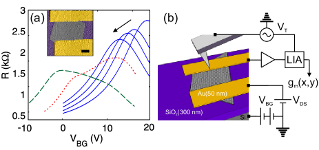
Our SGM setup is shown in Fig. 1(b) (see Ref.[26] for details.) To benefit from the high signal-to-noise ratio achievable using a.c. detection, we modulate the potential difference VT between the tip (Pt/Ir coated NanoWorld ARROW-NCPt) and the graphene at low frequency (typically 3 V @ 1 kHz) and detect the modulation of (250 A) using a lock-in amplifier. We quantify the demodulated component (0.1 A) by the local transconductance normalized to the bulk conductance .Crook et al. (2000)
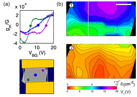
Figure 2(a) plots measured with the tip in each of the regions indicated in the diagram of the device (inset, Fig. 2.) is suppressed () at each tip position when 6 V. The opposite is true for 16 V, when is everywhere enhanced (). The crossover back-gate voltage (=0) falls within the range of intermediate and shows a sensitive dependence on tip position. To understand the basic form of the measured , we relate the conductivity of the (50 nm)2 region perturbed by the tipBerezovsky and Westervelt (2009) to a local carrier density by , where is the capacitive coupling between the tip and graphene, and is the local impurity-induced charge density.Adam et al. (2007); Chen et al. (2009b); Rossi et al. (2009) Neglecting quantum contributions to the conductivity, is proportional to , which changes sign at the local NP when (since =0). Hence is a measure of , which can be empirically related to the impurity density via (1.2-1.3).Chen et al. (2009b) We explore by measuring with the tip positioned over a grid of points with pitch 300 nm and constructing the map of shown in panel 1 of Fig. 2(b). A band with 1011 cm-2 (6 V) runs across the flake parallel to the contacts, asymetrically flanked by regions with higher density close to the contacts, where 1011 cm-2 (16 V). This profile can be explained by assuming that it reflects the temperature distribution generated by ohmic heating during current annealing. The remanent distribution in this case suggests that energy is dissipated in the flake itself, while the contacts act as heat sinks. A similar temperature distribution was inferred from previous scanning probeMoser et al. (2007) and RamanFreitag et al. (2009) microscopy measurements, though here the asymmetry either side of the higher temperature region is more pronounced. The two values of V0 also coincide with the positions of the shoulder and the maximum of the bulk [red curve, Fig. 1(a)], confirming that these features originate from the mesoscopic inhomogeneity.
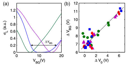
Figure 3(a) shows plots of the local conductivity reconstructed by numerically integrating [Fig. 2(a)]. Within the framework of Ref. [30], the width of the minimum conductivity plateau at the NP is expected to increase with .Adam et al. (2007); Chen et al. (2009b) While we did not observe this direct relationship, Fig. 3(b) reveals a linear correlation between and the spatial gradient of along parallel lines in the vicinity of the dashed line in Fig. 2(b). (We extract for each curve by subtracting the back-gate voltages where .) This is understandable as broadening is most pronounced when the tip gates both n- and p-type regions, in the same way that in homogeneous flakes is broadened by e-h puddles at low carrier density.Adam et al. (2007)
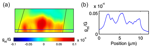
To assess the inhomogeneity remaining when , we annealed the flake at 1109 A/cm2 for 10 minutes and repeated the measurement of . The resulting map is shown in panel 2 of Fig. 2(b) and the corresponding sweep in Fig. 1(a)(green curve). In line with the previous analysis, the single peak in coincides with the average value of ( 2V) ( 1011 cm-2), and the greater homogeneity is reflected by the absence of the shoulder. However, upon close inspection we observe a region close to the top contact with 1011 cm-2. The doping in this region, which persisted even after annealing with 1109 A/cm2, is responsible for the remaining asymmetry in , since opposing changes in occur in regions with opposite carrier type.Blake et al. (2009) Figure 4(a) shows a raw (= 3 V) image of the flake after the second current anneal [c.f. green curve, Fig. 1(a)]. Such images provide complementary information to the maps of by allowing one to resolve finer variations directly via changes in . Superimposed on the micron-sized inhomogeneity are pronounced striations in that span the length of the flake with lateral period of 100 nm (see linescan, Fig. 4(b)). These modulations could be caused by enhanced heating from resistive hotspots in the disordered pn junctions formed close to the metal-graphene interface,Blake et al. (2009) or electromigration of material from the contacts.Moser et al. (2007) By inspecting the amplitude of the modulation in , we estimate that these striations reflect an impurity density fluctuation cm-2, which may impose an intrinsic limit to the homogeneity achievable when current annealing supported flakes.
In conclusion, SGM is a powerful method for characterizing the local conductivity of inhomogeneously doped graphene. We find that the local NP reflects the temperature distribution generated by ohmic heating and also exhibits finer linearly correlated inhomogeneities. Both types of inhomogeneity are likely to contribute to the e-h asymmetry observed in current-annealed flakes.
This work was financially supported by the European GRAND project (ICT/FET). ACF acknowledges funding from the European Research Grant NANOPOTS and the Royal Society.
References
- Geim and Novoselov (2007) A. K. Geim and K. S. Novoselov, Nature Materials 6, 183 (2007).
- Wang et al. (2009) X. Wang, X. Li, L. Zhang, Y. Yoon, P. K. Weber, H. Wang, and H. Dai, Science 324, 768 (2009).
- Han et al. (2007) M. Y. Han, B. Ozyilmaz, Y. Zhang, and P. Kim, Phys. Rev. Lett 98, 206805 (2007).
- Ozyilmaz et al. (2007) B. Ozyilmaz, P. Jarillo-Herrero, D. Efetov, and P. Kim, Appl. Phys. Lett. 91, 192107 (2007).
- Cervantes-Sodi et al. (2008) F. Cervantes-Sodi, G. Csanyi, S. Piscanec, and A. C. Ferrari, Phys. Rev. B 77, 165427 (2008).
- Chen et al. (2009a) Z. Chen, Y.-M. Lin, M. J. Rooks, and P. Avouris, Physica E 40, 228 (2009a).
- Deshpande et al. (2009) A. Deshpande, W. Bao, F. Miao, C. N. Lau, and B. J. LeRoy, Phys. Rev. B 79, 205411 (2009).
- Martin et al. (2008) J. Martin, N. Akerman, G. Ulbricht, T. Lohmann, J. Smet, K. V. Klitzing, and A. Yacoby, Nature physics 4, 144 (2008).
- Zhang et al. (2009) Y. Zhang, V. W. Brar, C. Girit, A. Zettl, and M. F. Crommie, Nature Physics 5, 722 (2009).
- Berezovsky and Westervelt (2009) J. Berezovsky and R. M. Westervelt, arXiv:0907.0428v1 (2009).
- Lee et al. (2008) E. J. H. Lee, K. Balusubramanian, R. T. Weitz, M. Burghard, and K. Kern, Nature Nanotechnology 3, 486 (2008).
- Mueller et al. (2009) T. Mueller, F. Xia, M. Freitag, J. Tsang, and P. Avouris, Phys. Rev. B. 79, 245430 (2009).
- Yu et al. (2009) Y.-J. Yu, Y. Zhao, S. Ryu, L. E. Brus, K. S. Kim, and P. Kim, Nano Lett. 9, 3430 (2009).
- Casiraghi et al. (2007a) C. Casiraghi, S. Pisana, K. S. Novoselov, A. K. Geim, and A. C.Ferrari, Appl. Phys. Lett. 91, 233108 (2007a).
- Stampfer et al. (2007) C. Stampfer, F. Molitor, D. Graf, K. Ensslin, A. Jungen, C. Hierold, and L. Wirtz, Appl. Phys. Lett. 91, 241907 (2007).
- Das et al. (2008) A. Das, S. Pisana, S. Piscanec, B. Chakraborty, S. K. Saha, U. V. Waghmare, R. Wang, H. R. Krishnamurthy, A. K. Geim, A. C. Ferrari, et al., Nature Nano. 3, 210 (2008).
- Novoselov et al. (2004) K. S. Novoselov, A. K. Geim, S. V. Morozov, D. Jiang, Y. Zhang, S. V. Dubonos, I. V. Grigorieva, and A. A. Firsov, Science 306, 666 (2004).
- Ponomarenko et al. (2009) L. A. Ponomarenko, R. Yang, T. M. Mohiuddin, M. I. Katsnelson, K. S. Novoselov, S. V. Morozov, A. A. Zhukov, F. Schedin, E. W. Hill, and A. K. Geim, Phys. Rev. Lett 102, 206603 (2009).
- Chen et al. (2009b) J. H. Chen, C. Jang, M. Ishigami, S. Xiao, W. G. Cullen, E. D. Williams, and M. S. Fuhrer, Solid State Communications 149, 1080 (2009b).
- Blake et al. (2009) P. Blake, R. Wang, S. V. Morozov, F. Schedin, L. A. Ponomarenko, A. A. Zhukov, R. R. Nair, I. V. Grigorieva, K. S. Novoselov, and A. K. Geim, Solid State Communications 149, 1068 (2009).
- Lohmann et al. (2009) T. Lohmann, K. von Klitzing, and J. H. Smet, Nano Lett. 9, 1973 (2009).
- Romero et al. (2008) H. E. Romero, N. Shen, P. Joshi, H. R. Gutierrez, S. A. Tadigadapa, J. O.Sofo, and P. C. Eklund, ACS Nano 2, 2037 (2008).
- Moser et al. (2007) J. Moser, A. Barriero, and A. Bachtold, Appl. Phys. Lett. 91, 163513 (2007).
- Bolotin et al. (2008) K. I. Bolotin, K. J. Sikes, Z. Jiang, M. Klima, G. Fudenberg, J. Hone, P. Kim, and H. L. Stormer, Solid State Communications 146, 351 (2008).
- Du et al. (2009) X. Du, I. Skachko, F. Duerr, A. Luican, and E. Y. Andrei, Nature 462, 192 (2009).
- Crook et al. (2000) R. Crook, C. G. Smith, C. G. Simmons, and D. A. Ritchie, J. Phys.: Condens. Matt. 12, L375 (2000).
- Casiraghi et al. (2007b) C. Casiraghi, A. Hartschuh, E. Lidorikis, H. Qian, H. Harutyunyan, T. Gokus, K. S. Novoselov, and A. C. Ferrari, Nano Lett. 7, 2711 (2007b).
- Ferrari et al. (2006) A. C. Ferrari, J. C. Meyer, V. Scardaci, C. Casiraghi, M. Lazzeri, F. Mauri, S. Piscanec, D. Jiang, K. Novoselov, S. Roth, et al., Phys. Rev. Lett 97, 187401 (2006).
- Farmer et al. (2009) D. B. Farmer, Y.-M. Lin, A. Afzali-Ardakani, and P. Avouris, Appl. Phys. Lett. 94, 213106 (2009).
- Adam et al. (2007) S. Adam, E. H. Hwang, V. M. Galitski, and S. D. Sarma, PNAS 104, 18392 (2007).
- Rossi et al. (2009) E. Rossi, S. Adam, and S. D. Sarma, Phys. Rev. B 79, 245423 (2009).
- Freitag et al. (2009) M. Freitag, M. Steiner, Y. Martin, V. Perebeinos, Z. Chen, J. C. Tsang, and P. Avouris, Nano Lett. 9, 1883 (2009).