Electron transport through a quantum
interferometer with side-coupled quantum dots: Green’s function
approach
Santanu K. Maiti1,2,∗
1Theoretical Condensed Matter Physics Division,
Saha Institute of Nuclear Physics,
1/AF, Bidhannagar, Kolkata-700 064, India
2Department of Physics, Narasinha Dutt College,
129 Belilious Road, Howrah-711 101, India
Abstract
We study electron transport through a quantum interferometer with side-coupled quantum dots. The interferometer, threaded by a magnetic flux , is attached symmetrically to two semi-infinite one-dimensional metallic electrodes. The calculations are based on the tight-binding model and the Green’s function method, which numerically compute the conductance-energy and current-voltage characteristics. Our results predict that under certain conditions this particular geometry exhibits anti-resonant states. These states are specific to the interferometric nature of the scattering and do not occur in conventional one-dimensional scattering problems of potential barriers. Most importantly we show that, such a simple geometric model can also be used as a classical XOR gate, where the two gate voltages, viz, and , are applied, respectively, in the two dots those are treated as the two inputs of the XOR gate. For (, the elementary flux-quantum), a high output current () (in the logical sense) appears if one, and only one, of the inputs to the gate is high (), while if both inputs are low () or both are high (), a low output current () appears. It clearly demonstrates the XOR gate behavior and this aspect may be utilized in designing the electronic logic gate.
PACS No.: 73.23.-b; 73.63.Rt.
Keywords: Quantum interferometer; Conductance; - characteristic; XOR gate; Anti-resonant state.
∗Corresponding Author: Santanu K. Maiti
Electronic mail: santanu.maiti@saha.ac.in
1 Introduction
Electronic transport in quantum confined systems like quantum rings, quantum dots, quantum wires, etc., has become a very active field both in the theoretical and experimental research. The present progress in nanoscience and technology has enabled us to use such quantum confined geometric models in electronic as well as spintronic engineering since these simple looking systems are the basic building blocks of designing nano devices. The key idea of manufacturing nano devices is based on the concept of quantum interference effect which is generally preserved throughout the sample of much smaller sizes, while, it disappears for larger systems. A mesoscopic normal metal ring is one such promising example where electronic motion is confined, and with the help of such a ring we can construct a quantum interferometer. In this article we will explore the electron transport properties through a quantum interferometer with side-coupled quantum dots, and show how such a simple geometric model can be used to design an XOR logic gate. To reveal this phenomenon we make a bridge system where the interferometer is attached symmetrically to two external electrodes, the so-called electrode-interferometer-electrode bridge. The theoretical progress of electron transport in a bridge system has been started after the pioneering work of Aviram and Ratner [1]. Later, many excellent experiments [2, 3, 4, 5, 6, 7] have been done in several bridge systems to justify the actual mechanisms underlying the electron transport. Though in literature many theoretical [8, 9, 10, 11, 12, 13, 14, 15, 16, 17, 18, 19, 20, 21, 22, 23, 24, 25, 26, 27] as well as experimental papers [2, 3, 4, 5, 6, 7] on electron transport are available, yet lot of discrepancies are still present between the theory and experiment. The electronic transport through the interferometer significantly depends on the interferometer-to-electrodes interface structure. By changing the geometry one can tune the transmission probability of an electron across the interferometer. This is solely due to the quantum interference effect among the electronic waves traversing through different arms of the interferometer. Furthermore, the electron transport through the interferometer can be modulated in other way by tuning the magnetic flux, the so-called Aharonov-Bohm (AB) flux, that threads the interferometer. The AB flux can change the phases of the wave functions propagating along the different arms of the interferometer leading to constructive or destructive interferences, and accordingly the transmission amplitude changes [28, 29, 30, 31, 32]. Beside these factors, interferometer-to-dots coupling is another important issue that controls the electron transport in a meaningful way. All these are the key factors which regulate the electron transmission in the electrode-interferometer-electrode bridge and these effects have to be taken into account properly to reveal the transport mechanisms.
The purposes of this paper are twofold. In the first part we explore the appearance of unconventional anti-resonant states for our model. These states are specific to the interferometric nature of the scattering and do not appear in ordinary scattering problems. While, the second part addresses the XOR gate response in this simple geometry. In our model, the interferometer, threaded by a magnetic flux , is directly coupled to two quantum dots, and two gate voltages and , are applied, respectively (see Fig. 1) in these dots. These gate voltages are treated as the two inputs of the XOR gate. Here we adopt a simple tight-binding model to describe the system and all the calculations are performed numerically. We narrate the XOR gate behavior by studying the conductance-energy and current-voltage characteristics as functions of the interferometer-to-dots coupling strengths, magnetic flux and gate voltages. Our study reveals that for a particular value of the magnetic flux, , a high output current () (in the logical sense) is available if one, and only one, of the inputs to the gate is high (), while if both the inputs are low () or both are high (), a low output current () appears. This phenomenon clearly demonstrates the XOR gate behavior which may be utilized in manufacturing the electronic logic gate. To the best of our knowledge the XOR gate response in such a simple system has not been described earlier in the literature.
The scheme of the paper is as follow. Following the introduction (Section ), in Section , we present the model and the theoretical formulations for our calculations. Section discusses the significant results, and finally, we conclude in Section .
2 Model and the synopsis of the theoretical background
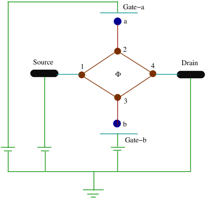
Let us start by referring to Fig. 1. A quantum interferometer, threaded by a magnetic flux , is attached symmetrically to two semi-infinite one-dimensional (D) metallic electrodes, viz, source and drain. Two quantum dots and (designed by filled blue circles) are directly coupled to the atomic sites and of the interferometer, respectively. These two quantum dots are subjected to the gate voltages and , respectively, those are regarded as the two inputs of the XOR gate. The gate voltages in the dots are given via the gate electrodes, viz, gate-a and gate-b. These gate electrodes are ideally isolated from the dots and can be regarded as two parallel plates of a capacitor. The actual scheme of connections with the batteries for the operation of the XOR gate is clearly presented in the figure (Fig. 1), where the source and the gate voltages are applied with respect to the drain.
To calculate the conductance of the interferometer with side-coupled quantum dots, we use the Landauer conductance formula [33, 34].
At very low temperature and bias voltage, the conductance can be expressed in terms of the transmission probability of an electron through the interferometer as,
| (1) |
This transmission probability can be represented in terms of the Green’s function of the interferometer including the dots and its coupling to the two electrodes by the relation [33, 34],
| (2) |
where and are respectively the retarded and advanced Green’s functions of the interferometer with the side-attached quantum dots including the effects of the two electrodes. The factors and describe the coupling of the interferometer to the source and drain, respectively. For the complete system i.e., the interferometer with the coupled quantum dots, source and drain, the Green’s function is defined as,
| (3) |
where . is the injecting energy of the source electron and gives an infinitesimal imaginary part to . To Evaluate this Green’s function, the inversion of an infinite matrix is needed since the full system consists of the interferometer with four atomic sites and two coupled quantum dots, and the two semi-infinite D electrodes. However, the entire system can be partitioned into sub-matrices corresponding to the individual sub-systems and the Green’s function for the interferometer with side-coupled quantum dots can be effectively written as,
| (4) |
where corresponds to the Hamiltonian of the interferometer with the two dots. Within the non-interacting picture it can be expressed in the form,
| (5) | |||||
In this Hamiltonian ’s are the site energies for all the sites except the sites and where the gate voltages and are applied, those are variable. These gate voltages can be incorporated through the site energies as expressed in the above Hamiltonian. () is the creation (annihilation) operator of an electron at the site and is the hopping integral between the nearest-neighbor sites of the interferometer. is the phase factor due to the flux threaded by the interferometer. The factors and correspond to the coupling strengths of the quantum dots and to the atomic sites and of the interferometer, respectively. For the two semi-infinite D perfect electrodes, a similar kind of tight-binding Hamiltonian is also used, except the phase factor , where the Hamiltonian is parametrized by constant on-site potential and nearest-neighbor hopping integral . The hopping integral between the source and the interferometer is , while it is between the interferometer and the drain. The parameters and in Eq. (4) represent the self-energies due to the coupling of the interferometer to the source and drain, respectively, where all the information of the coupling are included into these two self-energies [33].
The current () passing through the interferometer is depicted as a single-electron scattering process between the two reservoirs of charge carriers. The current can be evaluated as a function of the applied bias voltage by the relation [33],
| (6) |
where is the equilibrium Fermi energy. Here we make a realistic assumption that the entire voltage is dropped across the interferometer-electrode interfaces, and it is examined that under such an assumption the - characteristics do not change their qualitative features.
In this presentation, all the results are computed at absolute zero temperature. These results are also valid even for some finite (low) temperatures, since the broadening of the energy levels of the interferometer with side-coupled quantum dots due to its coupling with the electrodes becomes much larger than that of the thermal broadening [33]. On the other hand, at high temperature limit, all these phenomena completely disappear. This is due to the fact that the phase coherence length decreases significantly with the rise of temperature where the contribution comes mainly from the scattering on phonons, and accordingly, the quantum interference effect vanishes. Throughout the calculations we set , and choose the unit .
3 Results and discussion
We describe our results in two parts. In the first part, we narrate the existence of the anti-resonant states in this particular geometry those are specific to the interferometric nature of the scattering and do not occur in traditional one-dimensional scattering problems of potential barriers. On the other hand, in the second part, we demonstrate how this simple geometric model can be used as an XOR gate. The key controlling parameter for the whole operation of the XOR gate is the magnetic flux threaded by the interferometer.
As illustrative examples, in Fig. 2 we present the variation of the conductance (red curves) and the density of states (black curves) as a function of the energy for the interferometer with
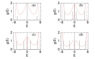
side-coupled quantum dots, considering the different values of the side-coupling strengths and , respectively. Here we set the site energies of all the atomic sites of the interferometer including the two dots as zero. Our results predict that, for some particular energies the conductances show resonance peaks (red curves), associated with the density of states (black curves). These energies are the so-called resonant energies, and the associated states are defined as the resonant states. The - spectra predict that, though the resonance peaks are available for some particular energies, but the electron conduction from the source to drain through the interferometer is possible almost for all other energies. This is due to the overlap of the two neighboring resonance peaks, where the contribution for the spreading of the resonance peaks comes from the imaginary parts of the self-energies and , respectively [33]. At the resonances, the conductance approaches the value , and therefore, for these energies the transmission probability goes to unity, since the
relation is satisfied from the Landauer conductance formula (see Eq. (1) with ). Now we interpret the dependences of the interferometer-to-dot coupling strengths on the electron transport. In Fig. 2(a), when there is no coupling between the interferometer and the two dots, the conductance shows non-zero value for the entire energy range. The situation becomes much more interesting as long as the coupling of the two dots with the interferometer is introduced. To illustrate it, in Figs. 2(b)-(d) we plot the results for the three different choices of the coupling strengths and , respectively. The introduction of the side-coupling provides the anti-resonant state. For all these three different choices of and , the conductance spectra (Figs. 2(b)-(d)) show that the conductance drops exactly to zero at the energy . At this particular energy, the density of states has a sharp peak, and it is examined that the height of this particular peak increases very rapidly as we decrease the imaginary part to the energy . It reveals that the electron conduction through this state is no longer possible, and the state is the so-called anti-resonant state. With the increase of the side-coupling strength, the width of the resonance peaks gradually decreases, as clearly observed from these figures. Both these resonant and anti-resonant states are associated with the energy eigenvalues of the interferometer including the two side-coupled dots, and thus, we can say that the conductance spectrum reveals itself the electronic structure of the interferometer including the two dots.
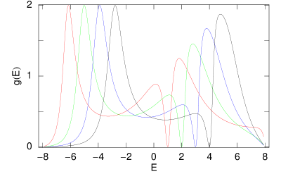
To examine the dependence of the anti-resonant state on the site energies of the interferometer and the two side-attached quantum dots, in Fig. 3 we plot the - characteristics for the four different cases of these site energies. The red, green, blue and black curves correspond to the results when the energies of the six atomic
sites (four sites of the interferometer and the two sites of the dots) are identically set to , , and , respectively. Quite interestingly we see that the anti-resonant state situates at these respective energies. Our critical investigation also shows that no anti-resonant state will appear if the site energy of anyone of these six sites is different from the other sites. The similar behavior will be also observed for the case if anyone of the three hopping strengths , and is different from the other two. Thus it can be emphasized that the anti-resonant state will appear only when the site energies of all the six sites are identical to each other as well as the strengths of the three different hopping parameters (, and ) are same. In this context it is also important to note that, though all the results presented above are done only for the flux , but the positions of these anti-resonant states will not change at all in the presence of and no new significant feature will be observed for the description of the anti-resonant states.
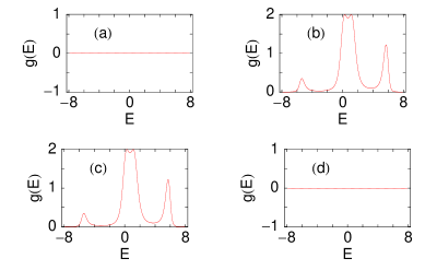
Next we concentrate our study on the XOR gate response exhibited by this geometric model. For the operation of the XOR gate, we set the magnetic
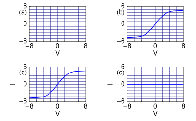
flux at i.e., in our chosen unit . As representative examples, in Fig. 4 we show the variation of the conductance as a function of the injecting electron energy , where (a), (b), (c) and (d) represent the results for the different cases of the gate voltages and applied in the two side-attached quantum dots, respectively. When both the two inputs and are identical to zero, i.e., both the two inputs are low, the conductance becomes exactly zero for the entire energy range (see Fig. 4(a)). This reveals that the electron conduction through the interferometer is not possible for this particular case. Similar behavior is also observed for the typical case when both the two inputs are high i.e., . In this situation also the electron conduction from the source to drain through the interferometer is not possible for the whole energy range (see Fig. 4(d)). On the other hand, for the rest two cases i.e., when any one of the two inputs is high and other one is low i.e., either and (Fig. 4(b)) or and (Fig. 4(c)), the conductance exhibits resonances for some particular energies. Thus for both these two cases the electron conduction takes place across the interferometer. Now we justify the dependences of the gate voltages on the electron transport for these four different cases. The probability amplitude of getting an electron across the interferometer depends on the quantum interference of the electronic waves passing through the upper and lower arms of the interferometer. For the symmetrically connected interferometer i.e., when the two arms of the interferometer are identical with each other, the probability amplitude is exactly zero () for the flux . This is due to the result of
| Input-I () | Input-II () | Current () |
the quantum interference among the two waves in the two arms of the interferometer, which can be obtained through the few simple mathematical steps. Thus for the cases when both the two inputs ( and ) are either low or high, the transmission probability drops to zero. While, for the two other cases, the symmetry of the two arms of the interferometer is broken by applying the gate voltage either in the dot or in , and therefore, the non-zero value of the transmission probability is achieved which reveals the electron conduction across the interferometer. Thus we can predict that the electron conduction takes place across the interferometer if one, and only one, of the two inputs to the gate is high, while if both the inputs are low or both are high the conduction is no longer possible. This feature clearly demonstrates the XOR gate behavior.
The XOR gate response can be much more clearly noticed by studying the - characteristics. The current passing through the interferometer is computed from the integration procedure of the transmission function as prescribed in Eq. (6). The transmission function varies exactly similar to that of the conductance spectrum, differ only in magnitude by the factor since the relation holds from the Landauer conductance formula Eq. (1). As representative examples, in Fig. 5 we display the variation of the current as a function of the applied bias voltage for the four different cases of the two gate voltages and . In the particular cases when both the two inputs are identical to each other, either low (Fig. 5(a)) or high (Fig. 5(d)), the current is zero for the complete range of the bias voltage . This behavior is clearly understood from the conductance spectra, Figs. 4(a) and (d), since the current is computed from the integration method of the transmission function . For the other two cases when only one of the two inputs is high and other is low, a high output current is obtained which are clearly described in Figs. 5(b) and (c). From these - curves the behavior of the XOR gate response is nicely observed. To make it much clear, in Table 1, we present a quantitative estimate of the typical current amplitude, computed at the bias voltage . It shows that, only when any one of the two inputs is high and other is low, while for the other cases when either or , the current achieves the value .
4 Concluding remarks
To summarize, we have studied electron transport in a quantum interferometer with side-coupled quantum dots. The interferometer, threaded by a magnetic flux , is attached symmetrically to two semi-infinite D metallic electrodes and two gate voltages, viz, and , are applied, respectively, in the two dots those are treated as the two inputs of the XOR gate. The system is described by the tight-binding Hamiltonian and all the calculations are done in the Green’s function formalism. We have numerically computed the conductance-energy and current-voltage characteristics as functions of the interferometer-to-dots coupling strengths, magnetic flux and gate voltages. We have described the essential features of the electron transport in two parts. In the first part, we have addressed the existence of the anti-resonant states, those are not available in the traditional scattering problems of potential barriers. On the other hand, in the second part, we have explored the XOR gate response for this particular model. Very interestingly we have noticed that, for the half flux-quantum value of (), a high output current () (in the logical sense) appears if one, and only one, of the inputs to the gate is high (). On the other hand, if both the two inputs are low () or both are high (), a low output current () appears. It clearly demonstrates the XOR gate behavior, and, this aspect may be utilized in designing a tailor made electronic logic gate.
The importance of this article is concerned with (i) the simplicity of the geometry and (ii) the smallness of the size. To the best of our knowledge the XOR gate response in such a simple low-dimensional system has not been addressed earlier in the literature.
References
- [1] A. Aviram and M. Ratner, Chem. Phys. Lett. 29, 277 (1974).
- [2] A. W. Holleitner, R. H. Blick, A. K. Hüttel, K. Eberl, and J. P. Kotthaus, Science 297, 70 (2002).
- [3] K. Kobayashi, H. Aikawa, S. Katsumoto, and Y. Iye, Phys. Rev. Lett. 88, 256806 (2002).
- [4] Y. Ji, M. Heiblum, and H. Shtrikman, Phys. Rev. Lett. 88, 076601 (2002).
- [5] A. Yacoby, M. Heiblum, D. Mahalu, and H. Shtrikman, Phys. Rev. Lett. 74, 4047 (1995).
- [6] J. Chen, M. A. Reed, A. M. Rawlett, and J. M. Tour, Science 286, 1550 (1999).
- [7] M. A. Reed, C. Zhou, C. J. Muller, T. P. Burgin, and J. M. Tour, Science 278, 252 (1997).
- [8] P. A. Orellana, M. L. Ladron de Guevara, M. Pacheco, and A. Latge, Phys. Rev. B 68, 195321 (2003).
- [9] P. A. Orellana, F. Dominguez-Adame, I. Gomez, and M. L. Ladron de Guevara, Phys. Rev. B 67, 085321 (2003).
- [10] A. Nitzan, Annu. Rev. Phys. Chem. 52, 681 (2001).
- [11] A. Nitzan and M. A. Ratner, Science 300, 1384 (2003).
- [12] Z. Bai, M. Yang, and Y. Chen, J. Phys.: Condens. Matter 16, 2053 (2004).
- [13] V. Mujica, M. Kemp, and M. A. Ratner, J. Chem. Phys. 101, 6849 (1994).
- [14] V. Mujica, M. Kemp, A. E. Roitberg, and M. A. Ratner, J. Chem. Phys. 104, 7296 (1996).
- [15] D. Zhang, J. Ma, H. Li, S. Fu, and X. Wang, Phys. Lett. A 372, 3085 (2008).
- [16] K. Walczak, Phys. Stat. Sol. (b) 241, 2555 (2004).
- [17] K. Walczak, arXiv:0309666.
- [18] W. Y. Cui, S. Z. Wu, G. Jin, X. Zhao, and Y. Q. Ma, Eur. Phys. J. B. 59, 47 (2007).
- [19] D. I. Golosov and Y. Gefen, Phys. Rev. B 74, 205316 (2006).
- [20] T. Kubo, Y. Tokura, T. Hatano, and S. Tarucha, Phys. Rev. B 74, 205310 (2006).
- [21] T. Nakanishi, K. Terakura, and T. Ando, Phys. Rev. B 69, 115307 (2004).
- [22] O. Entin-Wohlman, Y. Imry, and A. Aharony, Phys. Rev. B 70, 075301 (2004).
- [23] K. Kobayashi, H. Aikawa, S. Katsumoto, and Y. Iye, Phys. Rev. Lett. 88, 256806 (2002).
- [24] B. Kubala and J. König, Phys. Rev. B 65, 245301 (2002).
- [25] S. K. Maiti, Solid State Phenomena 155, 71 (2009).
- [26] S. K. Maiti, Solid State Commun. 149, 1684 (2009).
- [27] S. K. Maiti, Solid State Commun. 149, 1623 (2009).
- [28] R. Baer and D. Neuhauser, J. Am. Chem. Soc. 124, 4200 (2002).
- [29] D. Walter, D. Neuhauser, and R. Baer, Chem. Phys. 299, 139 (2004).
- [30] K. Tagami, L. Wang, and M. Tsukada, Nano Lett. 4, 209 (2004).
- [31] K. Walczak, Cent. Eur. J. Chem. 2, 524 (2004).
- [32] R. Baer and D. Neuhauser, Chem. Phys. 281, 353 (2002).
- [33] S. Datta, Electronic transport in mesoscopic systems, Cambridge University Press, Cambridge (1997).
- [34] M. B. Nardelli, Phys. Rev. B 60, 7828 (1999).