Carrier-induced refractive index change and optical absorption
in wurtzite InN and GaN: Fullband approach
Abstract
Based on the full band electronic structure calculations, first we consider the effect of -type doping on the optical absorption and the refractive index in wurtzite InN and GaN. We identify quite different dielectric response in either case; while InN shows a significant shift in the absorption edge due to -type doping, this is masked for GaN due to efficient cancellation of the Burstein-Moss effect by the band gap renormalization. Moreover, for high doping levels the intraband absorption becomes significant in InN. For energies below 1 eV, the corresponding shifts in the real parts of the dielectric function for InN and GaN are in opposite directions. Furthermore, we observe that the free-carrier plasma contribution to refractive index change becomes more important than both band filling and the band gap renormalization for electron densities above 1019 cm-3 in GaN, and 1020 cm-3 in InN. As a result of the two different characteristics mentioned above, the overall change in the refractive index due to -type doping is much higher in InN compared to GaN, which in the former exceeds 4% for a doping of 1019 cm-3 at 1.55 m wavelength. Finally, we consider intrinsic InN under strong photoexcitation which introduces equal density of electron and holes thermalized to their respective band edges. The change in the refractive index at 1.55 m is observed to be similar to the -doped case up to a carrier density of 1020 cm-3. However, in the photoexcited case this is now accompanied by a strong absorption in this wavelength region due to intravalence band transition. Our findings suggest that the alloy composition of InxGa1-xN can be optimized in the indium-rich region so as to benefit from high carrier-induced refractive index change while operating in the transparency region to minimize the losses. These can have direct implications for InN-containing optical phase modulators and lasers.
pacs:
78.20.Ci, 78.20.Bh, 78.40.FyI Introduction
The research efforts on InN and In-rich InGaN have been intensifying worldwide. As well as their traditional applications on solid-state lightning and lasers, new possibilities begin to flourish such as photovoltaics and chemical sensing.wu09 From the electronic structure point of view, InN has a number of unique properties.rinke Its band gap for the wurtzite phase is commensurate with the 1.55 m wavelength for fiber optics when it forms an alloy with a small amount of GaN. Furthermore, the small conduction band effective mass enables interesting band-filling effects. Even though the latter giving rise to Burstein-Moss effectburstein54 ; moss54 was the center of focus in the recent re-assessment of the high quality InN samples,wu02a ; davydov ; wu02b ; wu04 its device implications have not been given the full attention it deserved. Among the viable applications are the carrier-induced optical phase modulators,vinchant and tunable Bragg reflector and filters.deppe ; weber These devices are expected to play essential role, for instance, for the signal processing directly in the optical domain in the future high bit rate optical communication networks.
It was known from the early days of edge-emitting semiconductor lasers that carrier-induced refractive change affects the optical beam quality,kirkby77 such as mode guiding along the junction plane, self-focusing, filament formation, frequency chirping under direct modulation.olsson81 ; dutta84 The refractive index tunability by carrier injection was studied in the previous decade for the Indium-Group-V semiconductor compounds and alloys other than InN.bennett ; chusseau ; paskov97 In the case of InGaN laser structures, there have been recent theoreticalchow00 and experimentalschwarz03 ; rowe03 studies on the carrier-induced refractive index change and the linewidth enhancement factor. However, these studies considered only Ga-rich limit of InGaN alloys.
The purpose of this work is to offer a comparative theoretical account of carrier-induced refractive index change in both InN and GaN, so as to form a basis for the In-rich InGaN alloys. Primary attention is given to -type doping which is the prevalent type among the routinely grown samples.wu09 For the case of InN, the photoexcited bipolar carrier-induced dielectric effects are also examined. The crux of our study is based on the Bennett-Soref-Del Alamo approachbennett which includes band-filling, band gap renormalization (BGR) and plasma contributions. However, rather than a model band structure, we employ a rigorous full band technique to represent the band filling; preliminary account of this work was given in Ref. pssc08, . In Sec. II we present the theoretical details, this is followed by our results in Sec. III. A self-critique of our model and further discussions are provided in Sec. IV, ending with our conclusions in Sec. V. The Appendix contains our empirical pseudopotential parameters used for wurtzite InN.
II Theory
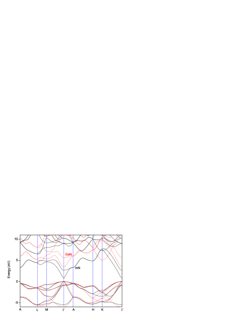
First, we would like to describe the electronic structure on which our computations are based. In the case of GaN, we use the local empirical pseudopotential method that we fitted to the existing experimental data, putting special emphasis on the conduction band behavior.prb00 For InN, we use the nonlocal empirical pseudopotential method, treating the angular-momentum channels and for In, and for N as nonlocal.sm04 Further details are given in the Appendix section. The corresponding band gap for InN comes out as 0.85 eV which agrees very well with the recent first principles resultscarrier05 ; bagayoko05 but it is higher than the 0.64 eV value established experimentally.wu09 Figure 1 shows the band structures of wurtzite InN and GaN.
As the Burstein-Moss effectburstein54 ; moss54 primarily shifts the absorption edge due to band filling, the ultimate quantity to be computed is the imaginary part of the optical (i.e., the long wavelength limit) dielectric tensor which is given in Gaussian units byhughes
| (1) | |||||
where are the Cartesian indices. , where is the momentum matrix element, is the free electron mass, , where is the energy of the band , at the wave vector k. The specific band label () represents filled (unfilled) bands, where for the clean cold semiconductors, the band occupation factors are taken as either one or zero. The volume integration in Eq. (1) is over the first Brillouin zone (BZ) which can be reduced to the irreducible BZ using the symmetry relations of the BZ (see, Fig. 2).
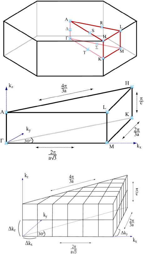
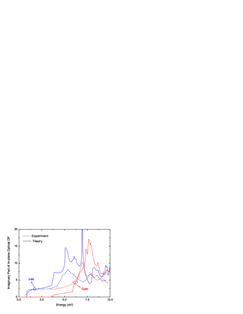
The Dirac delta term in Eq. (1) automatically reduces the volume integration to a surface formed by the k points which allow direct (vertical) transitions from a filled state to an unfilled state with an energy difference corresponding to the chosen photon energy. Such surface integrations routinely appear in the density of states, effective mass and response function calculations.martin-book They can be efficiently calculated numerically using the Lehmann-Taut method.lehmann This technique has also been shown to work for the second-order nonlinear optical response functionmoss87 and also for the full band phonon scattering rate calculation.prb00 In this work, for the required accuracy, we divide the irreducible BZ into a mesh of along the basal plane and the -axis directions (see, Fig. 2). In Fig. 3, we show the imaginary part of the optical dielectric function for the intrinsic (i.e., undoped) InN and GaN. The ordinary tensor component which corresponds to the electric field parallel to basal plane of the hexagonal crystal (i.e., in-plane) polarization is shown. For GaN, we observe a discrepancy between the theoretical and experimentalbenedict values close to the band edge. On the other hand, our theoretical result for InN matches well with the rigorous first-principles studies,furthmuller ; jin07 and also in reasonable agreement with the experiment.goldhahn
Another physical mechanism that accompanies band-filling is the BGR due to many-body interactions among the carriers.berggren In highly -doped InN samples it is observed that this partially cancels the Burstein-Moss effect.wu02b The electron-electron and electron-ion contributions within the random phase approximation are given in Gaussian units byberggren ; wu02b
| (2) | |||||
| (3) |
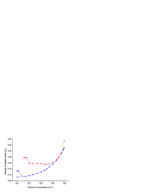
where is the electron (ion) density and is the static permittivity for which we use the experimental value of 9.5 (15.3) for GaN (InN).azuhata ; zubrilov and are, respectively, the Fermi and Thomas-Fermi wave numbers, is the effective Bohr radius in Å, is the conduction band effective mass. The latter quantity rapidly deviates with increase of energy from its band edge value, especially in the case of InN. Therefore, in these expressions we use an energy-dependent density of states effective mass value corresponding to the level of band-filling. Figure 4 shows for the conduction band these values used in this work for InN and GaN. The curve for InN is taken from the first-principles results.carrier05 For GaN, it has been computed using the same Lehmann-Taut method, but with a finer grid than used above, such as or more. In the case of photoexcitation which we consider for InN, actually we have a two-component quantum system (i.e., electron and hole gases). In the interests of simplicity, we adapt Eq. (2) by replacing the electron effective mass with the reduced electron-hole effective mass, given by where and are the energy-dependent electron and hole effective masses, respectively. The latter is almost constant for the densities dealt in this work and therefore is taken to be 0.84 for InN.
Having determined the imaginary dielectric function of a semiconductor with partially filled band(s), subject to BGR, the next aim is to compute their effect on the refractive index. Their interrelation is established by the causality principle which has to be satisfied by any physical response function.klingshirn In mathematical terms, this is governed by the Kramers-Kronig relation; for the real part, the corresponding expression, suppressing the Cartesian indices is given by
| (4) |
Computationally, it requires the knowledge of the imaginary part of the dielectric function for all energies; we have verified the convergence of our results by including 60 bands and accounting for the higher energy behavior (above 30 eV) analytically with a fall off.
Based on the mechanisms described above, carrier injection essentially leads to a change in the refractive index. Another significant contribution to the refractive index change is caused by the plasma absorption of the free carriers: electrons in the conduction band for the -doped case or the electrons and holes for the photoexcited case. Its resultant contribution can be expressed in convenient units asbennett
| (5) |
where is the refractive index of the intrinsic semiconductor, is the energy in eV, is the free-carrier density in cm-3 and is the effective mass in units of ; in the photoexcited case, for the latter two we use the electron-hole density and the effective mass (), respectively.
III Results
III.1 -doped case in InN and GaN
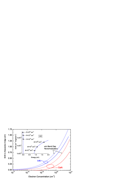
We first start with the -doped case which is quite easily achieved (sometimes even unintentionally) in InN and GaN and, we explore the filling of the conduction band by electrons fully ionized from their dopants. The electron concentrations up to about 7 cm-3 (9 cm-3) are considered marking the threshold beyond which the next higher conduction band starts to be filled for InN (GaN). Figure 5 shows the shift in the absorption edge due to Pauli blocking of the filled portions of the lowest conduction band. A marked contrast revealed with this plot is that the absorption edge shift in InN is much more significant compared to GaN. The disparity between the two materials’ conduction band edge density of state behavior plays a role here. While in InN the band-filling effect is quite strong, in the case of GaN this becomes smaller which is moreover effectively canceled by the BGR.
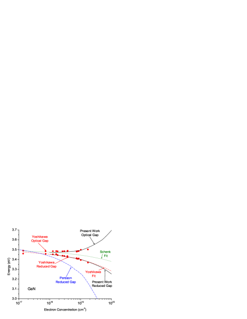
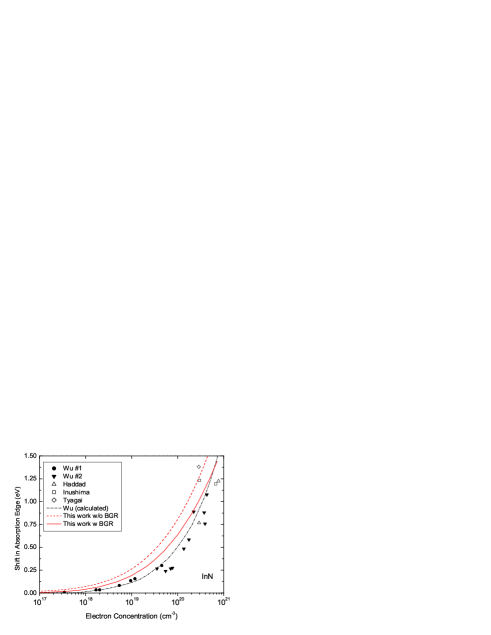
Yoshikawa et al. have used temperature-dependent photoluminescence spectroscopy to separate BGR and band-filling effects in Si doped GaN.yoshikawa99 Figure 6 illustrates the comparison of our -doped GaN results with this work for the reduced band gap, i.e., due to BGR, as well as for the optical gap which corresponds to the absorption edge including the BGR and Burstein-Moss effects. The dashed line is the fitted expression, eV offered by Yoshikawa et al. for the former. Very recently Schenk et al. relying on band edge luminescence peak and the line shape information have extracted an expression given by eV for the BGR in -doped GaN.schenk While our result closely agrees with the Yoshikawa data, Schenk’s expression is in disagreement with these. In Fig. 6, also a much more elaborate theoretical analysis for the BGR is shown which however deviates from the rest of these results.persson We believe that further studies are required to reach to a consensus over the BGR expression for GaN. The situation is more harmonious for InN. The comparison of our computed absorption shift for InN with the measurements and calculation from Wu et al.,wu04 together with other data mentioned in that worktyagai ; inushima ; haddad is provided in Fig. 7; it shows the overall agreement of our results with the literature.
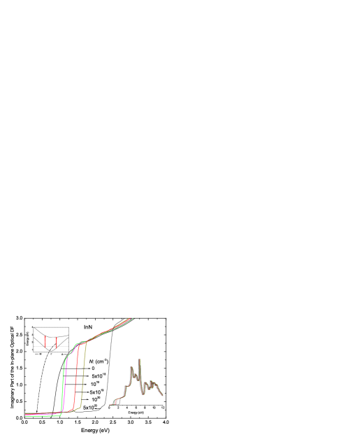
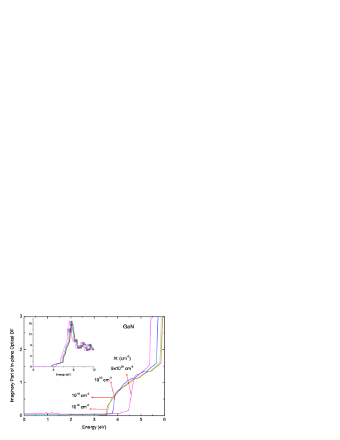
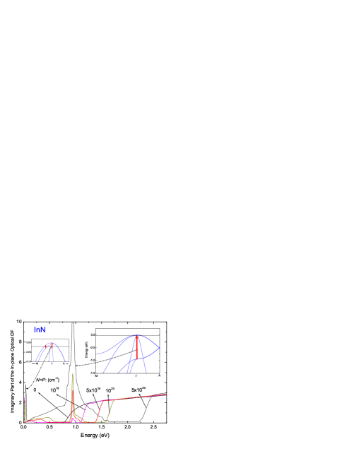
The conduction band filling and the associated BGR directly affect the imaginary part of the dielectric functions through the shift in the absorption edge deeper into the conduction band. This is illustrated for the ordinary components (i.e., the electric field lying on the crystal basal plane) for different electron concentrations in Figs. 8 and 9 for InN and GaN, respectively. It can be noticed for both cases, especially for larger dopings, that there is a nonzero absorption below the absorption edge, even down to zero energy. This is due to intraband absorption within the conduction band (see the upper inset in Fig. 8). The same behavior also appears in the measured InN samples.wu04
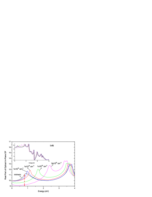
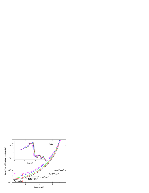
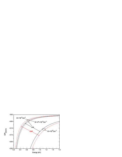
The real parts of the dielectric functions are obtained from the imaginary parts using the Kramers-Kronig relation in Eq. (4). The results are shown in Figs. 10 and 11 for InN and GaN, respectively. First of all, the real part of dielectric function of InN is more sensitive to -type doping. Furthermore, for low energies, the shifts are in opposite directions for InN and GaN, so that as the electron concentration increases, the permittivity decreases for InN, whereas it increases for GaN. Note that these are only the electronic contributions to polarization as Eq. (1) does not include the ionic degrees of freedom. Nevertheless the ions do not directly play a role in the change in the refractive index which is focus of this work. As mentioned in the Theory section, one should also add the free carrier plasma contribution to the refractive index [see, Eq. (5)]. This is separately shown in Fig. 12 which always has a negative contribution, and decreases as with energy .
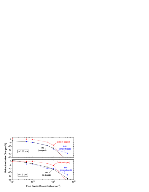
The overall change in the refractive index, including all of the effects mentioned so far is shown in Fig. 13. Because of their technological importance, it is evaluated at the two fiber-optic communication wavelengths of 1.55 and 1.3 m which correspond to energies of 0.8 and 0.954 eV, respectively; the former is marked with dashed vertical arrows in Figs. 10 and 11. It can be observed that the refractive index change due to -type doping is much higher in InN compared to GaN for both wavelengths. There are several reasons behind this outcome. First of all there is a cancellation that occurs for GaN; as shown in Fig. 5, BGR very effectively cancels the Burstein-Moss shift up to a density of 1019 cm-3. The lack of such a cancellation in InN is because of the very strong band-filling effect as a result of small density of states of InN close to conduction band edge, see the inset in Fig. 5. Furthermore, contrary to the case in InN, the refractive index change in GaN due to band filling is positive up to the ultraviolet. This is canceled by the negative plasma contribution [cf., Eq. (5)], which actually dominates beyond a density of 1019 cm-3 in GaN and 1020 cm-3 in InN.
Note that at the 1.3 m wavelength the intrinsic as well as doped InN display substantial interband absorption (see, Fig. 8), hence, in Fig. 13 we used the following generalization of the refractive index in the presence of loss:klingshirn
| (6) |
Because of this loss, 1.3 m case shows an overall reduction in the refractive index change compared to 1.55 m wavelength. As another curious point, the -doped InN curve in the bottom panel of Fig. 13 starts from a positive value which requires an explanation. Due to the absorption in the 1.3 m wavelength, the refractive index also peaks around the 0.95 eV range, particularly for the 1018 cm-3 density (cf. Fig. 10). Hence, the -doped InN curve in Fig. 13 becomes positive for this density as its refractive index exceeds that of the intrinsic sample. Even though the band-filling and plasma contributions try to reduce it, they are not as effective at this density.
III.2 Photoexcited case in InN
We would like to compare the pronounced refractive index change in -doped InN with the case where both electrons and holes are present. Since introducing holes with -type doping is still a major technical challenge in InN,wu09 we consider photodopingphotodoping where equal density of electrons and holes are generated by a strong photoexcitation. We further assume that these photocarriers quickly thermalize to their respective band edges and attain a degenerate quasiequilibrium distribution. Since the electron-hole pairs will eventually recombine within a time scale of 300-400 ps,chen03 the quasicontinuous optical excitation should replenish this in order to sustain the assumed steady-state carrier distribution. The associated quasi-Fermi levels for different electron-hole densities are marked in the inset of Fig. 5 which clearly indicates that the contribution of the holes to the Burstein-Moss effect is negligible. In Fig. 14 we show the imaginary dielectric function at several electron-hole densities. Compared to the -doped case in Fig. 8, we observe two new features around 0 and 0.94 eV which are caused by the intravalence band transitions: the former is due to very low energy transitions at the valence band maximum (left inset in Fig. 14), whereas the latter is the result of the transition (right inset in Fig. 14). It is the latter that makes a significant impact around 1.55 m (0.8 eV) and even more so at the 1.3 m wavelength (0.954 eV). Therefore, we would like to assert that our band structure agrees quite well with the other first-principle studiesbagayoko05 ; furthmuller which report the value 0.9 eV with the quasiparticle correction for the transition. As observed from Fig. 14, these new intravalence band channels refill the part of the spectra cleared by the Pauli blocking, undoing the Burstein-Moss effect. Also we can observe from Fig. 13 that below a carrier density of 1020 cm-3, the change in the refractive index at 1.55 m is seen to be very close to the -doped case. However, it should be recalled that this is now accompanied by a strong absorption (cf., Fig. 14) which can hamper its possible device applications.
IV A self-critique of the theoretical model and discussions
In this section we would like to discuss several aspects of the employed theoretical model both for the assertion of its general validity as well as for pointing out its possible improvements. To start with, all our results follow from the dielectric function expression of Eq. (1) which is obtained within the independent particle (i.e., random phase) approximation,ehrenreich and as such, it neglects the excitonic effects. In the case of intrinsic InN dielectric function, it has been shown by Furthmüller et al. that, apart from small shifts in the energy positions, these excitonic effects are responsible for the enhancement of some of the peaks in the spectra, predominantly close to the band edge, while the general shape remaining as unaffected.furthmuller Furthermore, in the presence of high concentration of free carriers, as considered in this work, the excitonic effects get perfectly screened. The transition from bound excitonic state to free electron-hole plasma takes place at the Mott critical density.klingshirn If we apply its estimate from Ref. bennett, , we get about 5 and 5 cm-3 for InN and GaN, respectively. Above these values, excitons will dissociate which is easily met for the density range of this study.
On the BGR, there are other theoretical estimations, such as the plasmon-polehaug and the Vashishta-Kaliavk models. However, we observed that when contrasted with the existing experimental data on GaNnagai and InN,schley the employed Berggren-Sernelius expressionberggren in this and recent studieswu02b ; wu04 outperforms these other models in the relevant high density range of this study. From a formal point of view, there exist more rigorous many-body approaches which incorporate excitons, BGR and band-filling effects in the same level, however, their formidable computational cost leads to a trade off with a simplistic effective mass band structure.lowenau
Furthermore, we should mention that the employed Berggren-Sernelius expression assumes a cubic crystal with parabolic bands.berggren These simplifications have been avoided by Persson and co-workers who have incorporated the electron-phonon contribution as well.persson Their framework is particularly better suited for handling the BGR under photoexcitation where both electron- and hole-gas many-body contributions can be individually included. However, as we stated previously, in the photoexcited case we still use the Berggren-Sernelius expression but with the reduced electron-hole effective mass. Essentially, the same discussion also applies for the plasma contribution in Eq. (5).
Compared to the available ab initio results for InN,rinke ; furthmuller ; carrier05 ; bagayoko05 our band structure is in good overall agreement. Nevertheless, there remain further discrepancies of most of these theoretical results from the experimental data. First of all, due to the fact that our computational band gap of 0.85 eV for InN is somewhat higher than the experimentally established value,wu09 we expect especially our 1.55 m wavelength data to be affected. However, this change should be more or less similar to the deviation between 1.55 m and 1.3 m cases in Fig. 13. In the case of GaN, our observation of a substantial deviation from the measured absorption in the vicinity of band gap (see, Fig. 3) calls for improvement on pseudopotential form factors for GaN which were originally optimized for high-field transport applications.prb00 Furthermore, we do not include the band tail (Urbach’s tail) absorption from the impurity states forming bands below the band edge.shen02 ; arnaudov Just like the excitons, the effect of localized states become marginal for high free-carrier densities, like beyond 1018 cm-3. Moreover, the characteristic Urbach energy parameter in high-quality InN samples turn out to be as low as 7.5 to 15 meV which indicates that these features are anchored to just below the band gap.klochikhin
Being intended as a bulk study, this work neglects any surface effects, the most important of which is the surface charge accumulation causing built-in electric field and band bending.lu03 ; mahboob In this regard, it has been mentioned by Kudrawiec et al. that for -type InN layer since the region of strong band bending is the surface electron accumulation layer, it will not affect absorptionlike techniques such as photoreflectance spectroscopy due to band filling of the conduction band.kudrawiec Another effect discarded in this study is the thermal smearing of the degenerate carrier statistics. As a possible follow up of this work it can be readily included, nevertheless we do not expect any marked deviations. Even though the quasi-Fermi level shift in the valence band is of the same order as the thermal energy (cf., inset of Fig. 5), as shown above, the main effect is driven by the Fermi level shift in the conduction band, which by far outweighs any thermal energy well up to room temperature for the carrier densities important for this work. Stemming from these idealizations, our main results in Fig. 13 should be taken as upper bounds. The list of these simplifications also suggests possible improvements of this work.
To harness the carrier-induced refractive index change such as in phase modulators, the associated losses need to be minimized. In this respect, the narrow 0.64 eV band gap of InN becomes undesirable for the 1.55 and 1.3 m applications as they enable supra band gap excitations where additional losses set in, especially for the photoexcited case. Our comparative study here suggests that the InxGa1-xN can enjoy both the high carrier-induced refractive index sensitivity while at the same time operating in the transparency region of the alloy. The poor sensitivity of GaN to carrier-induced refractive index change, as demonstrated by this work points towards the choice of indium-rich alloys.
V Conclusions
We have shown that based on a full band theoretical analysis, under -type doping, InN and GaN should display different dielectric characteristics. The absorption edge shift is masked in GaN, whereas it is highly pronounced in InN. For energies below 1 eV, the corresponding shifts in the real parts of the dielectric function for InN and GaN are in opposite directions. The free-carrier plasma contribution to refractive index becomes dominant above 1020 cm-3 for the case of InN. At a wavelength of 1.55 m, we predict more than 4% of change in the refractive index for InN for a doping of 1019 cm-3. Under optical pumping which fills the conduction and valence band edges with electrons and holes of equal density, the refractive index is not further affected by the presence of the holes. However, its major consequence is the increased intravalence band aborption as a result of transition. Beyond a hole density of 1019 cm-3, this affects 1.3 to 1.55 m wavelengths. We believe that this wide tunability of the index of refraction in InN by the conduction band electrons is technologically important for applications such as optical phase modulators. In the presence of holes, the valence band absorption needs to be taken into account, such as in the design of InN-based lasers for fiber-optics applications. Our findings suggest that the alloy composition of InxGa1-xN can be optimized in the indium-rich region so as to benefit from high carrier-induced refractive index change while operating in the transparency region to minimize the losses.
Acknowledgements.
The authors would like to thank the British Council for supporting the partnership of the Essex and Bilkent Universities. CB and CMT would like to thank the EU FP7 Project UNAM-Regpot Grant No. 203953 for partial support.| Å | |
| Å | |
| Ry |
| =5.55440, | =0.195168 |
| =4.51525, | =0.132069 |
| =3.64897, | =0.089251 |
*
Appendix: Empirical Pseudopotential Parameters for wurtzite InN
In the light of recent experimental and first-principles studies on wurtzite InN, we have expressed the local empirical pseudopotential method (EPM) form factors using the following functional form,
| (7) | |||||
| (8) |
where and are the symmetric and antisymmetric form factors in Rydbergs, is the wave number in units of with being the lattice constant in the hexagonal plane, and , are the fitting parameters which are listed in Table I.
The nonlocal part of the pseudopotential is based on the classical work of Chelikowsky and Cohen,cc with the plane-wave matrix elements being given by
| (9) | |||||
where is the structure factorcc for the atomic species , and is the Legendre polynomial corresponding to angular-momentum channel , is the atomic volume (i.e., primitive cell volume divided by number of atoms), , , and
| (10) |
here, is the spherical Bessel function, is (angular-momentum-dependent) well width. For InN, we treat the angular-momentum channels and for In, and for N as nonlocal. Table II lists InN nonlocal EPM parameters.
References
- (1) J. Wu, J. Appl. Phys. 106, 011101 (2009).
- (2) P. Rinke, M. Winkelnkemper, A. Qteish, D. Bimberg, J. Neugebauer, and M. Scheffler, Phys. Rev. B 77, 075202 (2008).
- (3) E. Burstein, Phys. Rev. 93, 632 (1954).
- (4) T. S. Moss, Proc. Phys. Soc. London, Sect. B 67, 775 (1954).
- (5) J. Wu, W. Walukiewicz, K. M. Yu, J. W. Ager III, E. E. Haller, H. Lu, W. J. Schaff, Y. Saito, and Y. Nanishi, Appl. Phys. Lett. 80, 3967 (2002).
- (6) V. Yu. Davydov, A. A. Klochikhin, R. P. Seisyan, V. V. Emtsev, S. V. Ivanov, F. Bechstedt, J. Furthmüller, H. Harima, A. V. Mudryi, J. Aderhold, O. Semchinova, and J. Graul, Phys. Status Solidi B 229, r1 (2002).
- (7) J. Wu, W. Walukiewicz, W. Shan, K. M. Yu, J. W. Ager, E. E. Haller, H. Lu, and W. J. Schaff, Phys. Rev. B 66, 201403(R) (2002).
- (8) J. Wu, W. Walukiewicz, S. X. Li, R. Armitage, J. C. Ho, E. R. Weber, E. E. Haller, H. Lu, W. J. Schaff, A. Barcz, and R. Jakiela, Appl. Phys. Lett. 84, 2805 (2004).
- (9) J.-F. Vinchant, J. A. Cavaillès, M. Erman, P. Jarry, and M. Renaud, J. Lightwave Technol. 10, 63 (1992).
- (10) D. G. Deppe, N. D. Gerrard, C. J. Pinzone, R. D. Dupuis, and E. F. Schubert, Appl. Phys. Lett. 56, 315 (1990).
- (11) J.-P. Weber, IEEE J. Quantum Electron. 30, 1801 (1994).
- (12) P.A. Kirkby, A. R. Goodwin, G. H. B. Thompson, and P. R. Selway, IEEE J. Quantum Electron. 13, 705 (1977).
- (13) A. Olsson and C. L. Tang, Appl. Phys. Lett. 39, 24 (1981).
- (14) N. K. Dutta, N. A. Olsson, and W. T. Tsang, Appl. Phys. Lett. 45, 836 (1984).
- (15) B. R. Bennett, R. A. Soref, and J. A. Del Alamo, IEEE J. Quantum Electron. 26, 113 (1990).
- (16) L. Chusseau, P. Martin, C. Brasseur, C. Alibert, P. Hervé, P. Arguel, and F. Lozes-Dupuy, Appl. Phys. Lett. 69, 3054 (1996).
- (17) P. P. Paskov, J. Appl. Phys. 81, 1890 (1997).
- (18) W. W. Chow, H. Amano, and I. Akasaki, Appl. Phys. Lett. 76, 1647 (2000).
- (19) U. T. Schwarz, E. Sturm, W. Wegscheider, V. Kümmler, A. Lell, and V. Härle, Appl. Phys. Lett. 83, 4095 (2003).
- (20) M. Röwe, P. Michler, J. Gutowski, V. Kümmler, A. Lell, and V. Härle, Phys. Status Solidi A 200, 135 (2003).
- (21) C. Bulutay and N. A. Zakhleniuk, Phys. Status Solidi C 5, 511 (2008).
- (22) C. Bulutay, B. K. Ridley, and N. A. Zakhleniuk, Phys. Rev. B 62, 15754 (2000).
- (23) C. Bulutay and B. K. Ridley, Superlattices Microstruct. 36, 465 (2004).
- (24) P. Carrier and S.-H. Wei, J. Appl. Phys. 97, 033707 (2005).
- (25) D. Bagayoko and L. Franklin, J. Appl. Phys. 97, 123708 (2005).
- (26) J. L. P. Hughes and J. E. Sipe, Phys. Rev. B 53, 10751 (1996).
- (27) R. M. Martin, Electronic Structure (Cambridge University Press, Cambridge, 2004).
- (28) G. Lehmann and M. Taut, Phys. Status Solidi B 54, 469 (1972).
- (29) D. J. Moss, J. E. Sipe, and H. M. van Driel, Phys. Rev. B 36, 1153 (1987).
- (30) R. Goldhahn, A. T. Winzer, V. Cimalla, O. Ambacher, C. Cobet, W. Richter, N. Esser, J. Furthmüller, F. Bechstedt, H. Lu, and W. J. Schaff, Superlattices Microstruct. 36, 591 (2004).
- (31) L. X. Benedict, T. Wethkamp, K. Wilmers, C. Cobet, N. Esser, E. L. Shirley, W. Richter, and M. Cardona, Solid State Commun. 112, 129 (1999).
- (32) J. Furthmüller, P. H. Hahn, F. Fuchs, and F. Bechstedt, Phys. Rev. B 72, 205106 (2005).
- (33) H. Jin, G. L. Zhao, and D. Bagayoko, J. Appl. Phys. 101, 033123 (2007).
- (34) K.-F. Berggren and B. E. Sernelius, Phys. Rev. B 24, 1971 (1981).
- (35) T. Azuhata, T. Sota, K. Suzuki, and S. Nakamura, J. Phys.: Condens. Matter 7, L129 (1995).
- (36) A. Zubrilov, in Properties of Advanced Semiconductor Materials GaN, AlN, InN, BN, SiC, SiGe, edited by M. E. Levinshtein, S. L. Rumyantsev, and M. S. Shur (Wiley, New York, 2001), pp. 49-66.
- (37) C. F. Klingshirn, Semiconductor Optics, 3rd ed. (Springer, Berlin, 2007).
- (38) M. Yoshikawa, M. Kunzer, J. Wagner, H. Obloh, P. Schlotter, R. Schmidt, N. Herres, and U. Kaufmann, J. Appl. Phys. 86, 4400 (1999).
- (39) H. D. P. Schenk, S. I. Borenstain, A. Berezin, A. Schön, E. Cheifetz, S. Khatsevich, and D. H. Rich, J. Appl. Phys. 103, 103502 (2008).
- (40) C. Persson, B. E. Sernelius, A. Ferreira da Silva, C. Moyseś Arauj́o, R. Ahuja, and B. Johansson, J. Appl. Phys. 92, 3207 (2002).
- (41) V. A. Tyagai, A. M. Evstigneev, A. N. Krasiko, A. F. Andreeva, and V. Ya. Malakhov, Sov. Phys. Semicond. 11, 1257 (1977).
- (42) T. Inushima, T. Yaguchi, A. Nagase, A. Iso, and T. Shiraishi, Inst. Phys. Conf. Ser. 142, 971 (1996); T. Inushima, T. Shiraishi, and V. Yu. Davydov, Solid State Commun. 110, 491 (1999).
- (43) D. B. Haddad, J. S. Thakur, V. M. Naik, G. W. Auner, R. Naik, and L. E. Wenger, Mater. Res. Soc. Symp. Proc. 743, L11.22 (2002).
- (44) There exists a somewhat different use of the “photodoping” terminology to describe the dissolution of metals, such as Ag or Cu, into chalcogenide glasses under an illumination. However, this is more appropriately termed as photodissolution.kolobov
- (45) F. Chen, A. N. Cartwright, H. Lu, and W. J. Schaff, Appl. Phys. Lett. 83, 4984 (2003).
- (46) H. Ehrenreich and M. H. Cohen, Phys. Rev. 115, 786 (1959).
- (47) H. Haug and S. W. Koch, Phys. Rev. A 39, 1887 (1989).
- (48) P. Vashishta and R. K. Kalia, Phys. Rev. B 25, 6492 (1982).
- (49) T. Nagai, T. J. Inagaki, and Y. Kanemitsu, Appl. Phys. Lett. 84, 1284 (2004).
- (50) P. Schley, R. Goldhahn, A. T. Winzer, G. Gobsch, V. Cimalla, O. Ambacher, H. Lu, W. J. Schaff, M. Kurouchi, Y. Nanishi, M. Rakel, C. Cobet, and N. Esser, Phys. Rev. B 75, 205204 (2007).
- (51) J. P. Löwenau, S. Schmitt-Rink, and H. Haug, Phys. Rev. Lett. 49, 1511 (1982); J. P. Löwenau, F. M. Reich, and E. Gornik, Phys. Rev. B 51, 4159 (1995).
- (52) W. Z. Shen, L. F. Jiang, H. F. Yang, F. Y. Meng, H. Ogawa, and Q. X. Guo, Appl. Phys. Lett. 80, 2063 (2002).
- (53) B. Arnaudov, T. Paskova, P. P. Paskov, B. Magnusson, E. Valcheva, B. Monemar, H. Lu, W. J. Schaff, H. Amano, and I. Akasaki, Phys. Rev. B 69, 115216 (2004).
- (54) A. Klochikhin, V. Davydov, V. Emtsev, A. Sakharov, V. Kapitonov, B. Andreev, H. Lu, and W. J. Schaff, Phys. Status Solidi A 203, 50 (2006).
- (55) H. Lu, W. J. Schaff, L. F. Eastman, and C. E. Stutz, Appl. Phys. Lett. 82, 1736 (2003).
- (56) I. Mahboob, T. D. Veal, C. F. McConville, H. Lu, and W. J. Schaff, Phys. Rev. Lett. 92, 036804 (2004).
- (57) R. Kudrawiec, T. Suski, J. Serafinćzuk, J. Misiewicz, D. Muto, and Y. Nanishi, Appl. Phys. Lett. 93, 131917 (2008).
- (58) J. R. Chelikowsky and M. L. Cohen, Phys. Rev. B 14, 556 (1976).
- (59) A.V. Kolobov and S.R. Elliott, Adv. Phys. 40, 625 (1991).