Electron transport and quantum-dot energy levels in Z-shaped graphene nanoconstriction with zigzag edges
Abstract
Motivated by recent advances in fabricating graphene nanostructures, we find that an electron can be trapped in -shaped graphene nanoconstriction with zigzag edges. The central section of the constriction operates as a single-level quantum dot, as the current flow towards the adjunct sections (rotated by ) is strongly suppressed due to mismatched valley polarization, although each section in isolation shows maximal quantum value of the conductance . We further show, that the trapping mechanism is insensitive to the details of constriction geometry, except from the case when widths of the two neighboring sections are equal. The relation with earlier studies of electron transport through symmetric and asymmetric kinks with zigzag edges is also established.
pacs:
73.63.-b, 73.22.Pr, 81.07.TaI Introduction
Soon after the breakthrough in its fabrication Gei04 ; Gei05 , an atomically-thin carbon monolayer (graphene) has attracted intense experimental and theoretical attention. An unusual band structure of graphene leads to exotic electronic properties Cas09 , which makes possible either to create devices that have no analogue in silicon-based electronics Gei07 , or to test various predictions of relativistic quantum mechanics in a condensed-matter system Bee08 . Additionally, graphene’s true two-dimensional nature combined with high carrier mobility makes it a promising base material for studying low dimensional systems, such as quantum wires realized as graphene nanoribbons Che07 ; Han07 ; Li08 ; Wan08 ; Sta09 , or quantum dots Sil07 ; Pon08 ; Gut08 . Just to give a recent example, the exotic features of quantum chaotic behavior, characteristic for massless spin- fermions confined in a quantum dot Ber87 , have been found both in an experiment Pon08 and computer simulations Wur09a .
Theoretical research on graphene nanostructures have started much earlier Fuj96 ; Nak96 ; Wak01 ; Mun06 but speed up after it was realized, that such systems are promising building blocks for a solid-state quantum computer Tra07 ; Ryc07 . In attempt to operate on a solid-state qubit Wol01 in graphene, one need to deal with an obstacle that electrons occur in two degenerate families, corresponding to the presence of two different valleys in the band structure. Trauzettel et al. Tra07 propose to solve this problem by using the insulating graphene nanoribbon with armchair edges, for which the valley degeneracy is lifted up by the boundary condition Two06 . Then, applying the gate voltage to a finite section of the ribbon, one forms the quantum dot which has a single relevant electronic level (with a spin-only degeneracy) for a considerably wide interval of electron Fermi energies, and thus is called a single-level quantum dot (SQD). As a fabrication of perfect armchair nanoribbon seems to be difficult due to the edge instability Gas08 ; Hua09 an alternative approaches, employing simultaneously external magnetic field and the mass confinement to break valley degeneracy in graphene rings Rec07 ; Zar09 , disks Rec09 , or antidots Ped08 ; She08 , have been discussed. The operational simplicity of the device Tra07 , offering a fully-electrostatic control, has inspired designing its counterpart based on a nanoribbon with predominantly zigzag edges Wan07 , similar to these already obtained in well-controlled fabrication processes Han07 ; Li08 ; Wan08 . An additional motivation to focus on ribbons with zigzag edges comes from the two theoretical findings: local-density approximation results Son06 show that the electronic structure narrow graphene constrictions can be well described by a simple tight binding model, and analytical discussion of the tight-binding equations for a semi-infinite honeycomb lattice Akh08a shows that the zigzag boundary condition applies generically (at low energies) to arbitrary lattice termination, except from the case we have a perfect armchair edge.
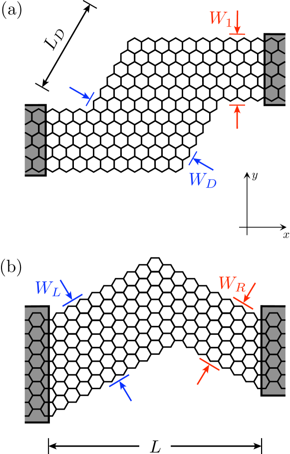
The device Wan07 , however, still needs sections of insulating ribbon with armchair edges, attached serially to both sides of the central section with zigzag edges (operating as SQD) to suppress the outward current flow. In this paper, we demonstrate numerically that a similar -shaped constriction, in which each of the three sections has zigzag edges (see Fig. 1(a)) and carries a fully conducting channel, may operate as highly-effective SQD due to mismatched valley polarization between the neighboring sections (rotated by ). The operation of such a double-kink device is rationalized by referring to the conductance spectrum of a single-kink device (Fig. 1(b)) which suppress the current Ryc08 , and by the discussion of level quantization for a finite section of the ribbon with zigzag edges Mal08 .
The paper is organized as follows: In Sec. II we briefly present the numerical method of the conductance calculation in a tight-binding model of graphene, and discuss its relation to the effective Dirac equation. Then, in Sec. III, we recall the idea of valley polarization in constrictions with zigzag edges leading to the current suppression in the kink device, and calculate numerically the conductance of kink devices with various geometries. Finally, in Sec. IV, two kinks are attached serially and the resonance transmission via quantum-dot levels is discussed.
II Tight binding model for electron transport in graphene
We start from the nearest-neighbor tight binding model taking into account the orbitals of carbon atoms Cas09 , with the Hamiltonian
| (1) |
The hopping matrix element if the orbitals and are nearest neighbors on the honeycomb lattice (with eV), otherwise . The electrostatic potential energy varies only along the -axis in the coordinate system of Fig. 1. It is chosen as in the leads marked by shadow areas ( or ) or in the device area (). For a given Fermi energy , the chemical potential is equal to or to , respectively. Throughout the paper, we analyze the system conductance as a function of at fixed such that corresponds to large number of propagating modes (the heavily-doped leads limit).
In the limit of zero bias voltage, phase-coherent transport properties of a noninteracting system such as described by the Hamiltonian (1) are encoded in the scattering matrix Dat97
| (2) |
which contains the transmission () and reflection () amplitudes for charge carries incident from the left (right) lead, respectively. The conductance is determined by the Landauer-Büttiker formula
| (3) |
where is the conductance quantum, and is the transmission probability for the -th normal mode. Apart from the simplest cases, when different transverse modes are not mixed by the transport Two06 ; Bre06 and the analytical solutions are available, one need to calculate the transmission matrix numerically. This can be achieved in two steps: First, we find the propagating modes in the leads , where denotes the -th incoming/outgoing mode in the -th lead, with their self-energies . Then, the scattering matrix (2) is obtained from the Lee-Fisher relation
| (4) |
The self-energy term represents the leads, with the coupling matrix of the leads to the contact region. The matrix contains normalization factors proportional to the propagating velocities for the modes. The direct matrix inversion in Eq. (4) is usually avoided by finding the matrix via the recursive Green’s function algorithm, also available in a version for a multi-terminal geometry Wim08 . For the two-terminal geometries considered here, and for the number of lattice sites , the direct matrix inversion with standard numerical routines is also very effective. According to Eq. (4), the transmission matrix depends on the properties of both constituents of the device under consideration: the leads and sample area. For the case of a weakly-doped graphene samples however, it was shown Sch07 that the transport of Dirac fermions is insensitive to the details of the leads, provided they carry a sufficiently large number of propagating modes.
The method of the conductance calculation in a tight binding model of graphene, described briefly above, represents an adaptation—to the honeycomb lattice—of the method developed by Ando for a square lattice And91 . Albeit technically similar, from the fundamental point of view the two methods represents quite different approaches to mesoscopic physics. Ando’s approach starts from a discretization of the Schrödinger equation in order to solve the scattering problem for the geometries which are not tractable in a continuous limit. Here, we deal directly with the microscopic model of graphene, allowing one to extent the discussion on the situation when its effective model for low-energy excitations, given by the massless Dirac equation Cas09 , breaks down due to scattering the carriers between valleys Akh08b . A finite-difference method for solving the Dirac equation on a square lattice was also recently developed Two08 .
III The kink device with zigzag edges
III.1 Valley polarization and the electron transport
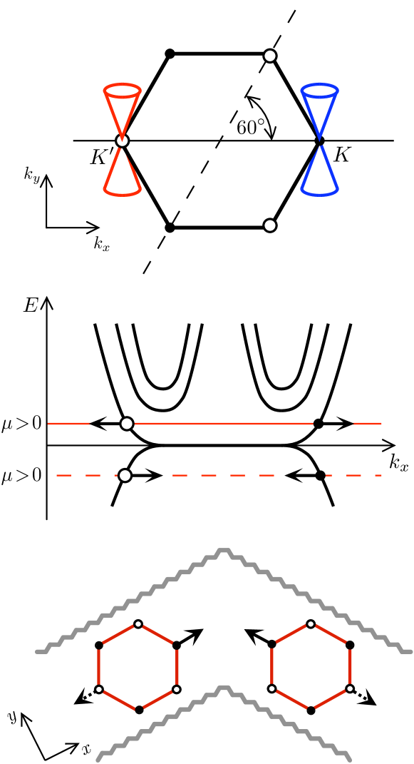
To understand the physics ruling the conductance of devices shown in Fig. 1, one needs first to recall basic facts concerning electron transport through the constriction with parallel zigzag edges: a building block of each device considered. Such a constriction, also known as the valley filter Ryc07 , was shown to produce, upon ballistic injection of current, the nonequilibrium valley polarization in a sheet of graphene attached. Motivated by the related analytical result for generic boundary conditions of graphene flakes Akh08a we have shown numerically Ryc08 , that valley polarization is also produced by constrictions with other edges, apart from the perfect armchair edges. These observations are rationalized as follows: For a constriction long enough, the transport become one-dimensional, and crystallographic orientation of edges determines the direction of propagation in the first Brillouin zone (see Fig. 2). As the lowest propagating mode in such a nanoribbon lack the twofold degeneracy of higher modes (and may be arbitrary close to one of the Dirac points or ) the crystallographic orientation also determines the valley polarization of current passing the constriction (which is opposite for the conductance then for the valence band).
Now, the two quite different devices consisting of two valley filters (of the opposite polarity) in series, can be constructed. By simple applying a step-like potential profile to the straight ribbon with zigzag edges, one obtains the electrostatically-controlled valley valve Akh08b . Alternatively, one can build the kink device Ryc08 ; Iye08 . In both cases, the current suppression due to mismatched valley polarization produced by two constituents of the device, is expected. However, a bit more detailed discussion of the current-suppression mechanism on the example of the kink device (see Fig. 2, bottom panel) unveils its striking feature: Strictly speaking, a one-to-one correspondence between the direction of propagation and the valley index, appearing in a nanoribbon, causes the electron can neither be transmitted nor reflected by the interface between two filters of opposite polarity! The same observation applies to the valley valve, for which the theoretical analysis of microscopic tight-binding equations Akh08b shows, that the intervalley scattering processes lead to sinusoidal conductance oscillations around the mean value when rotating the interface line with respect to the ribbon edge. The valve conductance also depends on its width, and is significantly different for the cases when zigzag and anti-zigzag ribbons are used, illustrating the microscopic nature of an electron transport. For the kink device, an analytical solution is missing, and the existing numerical results are overviewed briefly below.
III.2 Conductance of the kink device
The scattering problem for devices similar to that shown in Fig. 1(b) have been studied independently by several authors. The perfectly symmetric kink, formed by two semi-infinite nanoribbons with zigzag edges each of which is carrying a single propagating mode, shows irregular conductance oscillations with varying chemical potential Iye08 . The oscillations cover the full range of , and the upper limit is approached when the resonances with quasi-bond states, localized at the kink symmetry axis, occur. The system of tight-binding equations describing the symmetric kink, however, was found to be numerically stable only for ribbons of a moderate width (in units of the lattice spacing ). In the case of an asymmetric kink with attached to heavily-doped graphene leads Ryc08 we have at the first conductance step, and the resonances do not appear. On the other hand, the kink-like system formed by joining the two ribbons rotated by shows almost a perfect transmission, as the mismatched-valley polarization does not appear in such a case Are07 .
Here, we consider a slightly different geometry then studied in Refs. Ryc08 ; Iye08 . Namely, the kink device is attached to heavily-doped graphene leads with armchair edges. This guarantees the reflection symmetry of the system when , and eliminates the problem with numerical stability occurring for wider ribbons in the setup of Ref. Iye08 . We have fixed the left ribbon width at , corresponding to the subband splitting and propagating modes for . The right ribbon width is varied as , , and .
The operation of the kink device is demonstrated in Fig. 3. First, we took a sample area of the length and plot, in Fig. 3(a), the conductance as a function of the chemical potential. All three devices with different show some conductance suppression at the first plateau . The conductance of the symmetric kink () is still of the order of , but the asymmetric kinks shows much stronger suppression at low energies (see the inset). For an additional illustration we present, in Fig. 3(b), the conductance as a function of at fixed . For , we have , with the number of propagating modes in the right arm or (for or , respectively). For larger , first decrease exponentially, in order to saturate for (the length above which the role of evanescent modes becomes negligible) in the symmetric case. For , continues to decay and approaches the value for longest examined systems, confirming the claim of Ref. Ryc08 , that the asymmetric kink device in graphene blocks the current very effectively at low dopings. These findings also coincides with earlier results for Aharonov-Bohm quantum rings Rec07 ; Ryc09 for which intervalley scattering rate was shown to be related to the presence of an asymmetry or edge irregularities.
Away from the first plateau, each device shows conductance quantization that is essentially governed by the narrower arm width . In the symmetric case, however, we have the steps corresponding to even multiplicities of , whereas in the asymmetric case odd multiplicities appear. This can be summarize in an approximating formula for the kink conductance
| (5) |
where the Kronecker delta accounts for mismatched valley polarization of the lowest propagating modes in two kink arms, which affect the total conductance also at higher dopings.
IV Bound states of a double kink
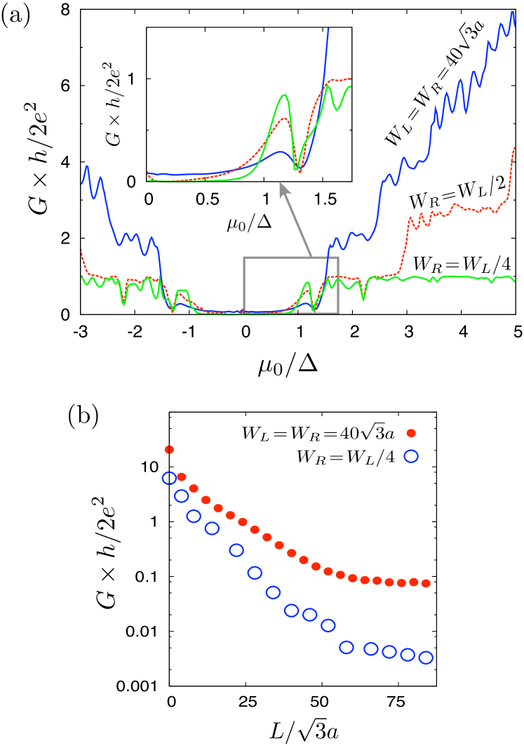
The conductance spectra of -shaped nanoconstriction of Fig. 1(a) are presented in Fig. 4. We consider three different devices, all built by joining finite sections of two nanoribbons with zigzag edges: one of the width, and the other of the width. In the first case, we arrange the building blocks in a double-kink setup, such that the central section is wider then the peripheral sections (, ). Next, we consider the setup of a uniform width (). Finally, we took the peripheral sections wider than the central one (, ). For each setup, the total sample area length is fixed at . The results show, either for the narrow-wide-narrow or for the wide-narrow-wide setup (see Figs. 4(a) and 4(c), respectively), that at the first conductance plateau except from the narrow peaks, corresponding to resonances with the quantum-dot states of the central section. Only for a uniformly-wide device some finite intervals of , for which , appear in Fig. 4(b).
These findings are related to the operation of the kink device studied in previous section as follows: The asymmetric kink blocks the current at low dopings, so two identical devices of its kind in series function as an electrostatically-controlled quantum dot (with an electron trapped between the kinks) regardless we join together wider, or narrower of the kink arms. The two symmetric kinks in series may also trap an electron accidentally, when the eigenstate of the central section lies in an energy interval, for which the single-kink conductance is low enough.
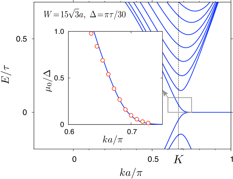
In Fig. 5, we plot the positions of the conductance maxima extracted from Fig. 4(c), together with the dispersion relation for an infinitely long nanoribbon of width. The -coordinate of each maximum is related to its number in sequence as , with determined via . (Notice that the first conductance maxima are blurred at finite machine precision due to the dispersionless character of the lowest subband). Strictly speaking, each bound state of the central ribbon section of length is given by a unique quantum superposition of propagating waves from and valleys Mal08 , the dispersion relation for one valley is, however, a mirror reflection of that for the second valley. The datapoints shown in the inset of Fig. 5 follow the dispersion relation for the lowest subband of a nanoribbon with zigzag edges. Hence, for each peak in the conductance spectrum of a double-kink device, the corresponding quantum-dot energy level is found.
V Conclusions
In conclusion, we have studied numerically the electron transport through -shaped nanoconstriction with zigzag edges, operating as a quantum dot in graphene. The device conductance, analyzed as a function of the chemical potential, exhibits a series of narrow resonance peaks. Each of the resonances is linked up to the energy level of the central section, when separated from the other parts of the device. An electron-trapping mechanism is discussed by analyzing the transport through a basic device building block: the kink with zigzag edges. A moderate current suppression is observed for the symmetric kink, whereas the asymmetric kink was found to reflect electrons almost perfectly. The role of a mismatched valley polarization on both sides of the kink is stressed.
Similar bound states were recently found in the simulation of transport through -shaped nanoribbon Wur09b with irregular edges. However, such a system contains finite sections of a nanoribbon with armchair edges, so the nature of the electron-trapping mechanism is not as clear as for the simpler system considered here.
Acknowledgment
I thank to Anton Akhmerov, Patrik Recher, C.W.J. Beenakker, İnanç Adagideli, Klaus Richter, Michael Wimmer, and Jürgen Wurm for helpful discussions and correspondence. The work was mainly completed during the Alexander von Humboldt (AvH) fellowship in Regensburg. Partial supports from the Polish Science Fundation (FNP) and the Polish Ministry of Science (Grant No. N–N202–128736) are acknowledged.
References
- (1) K.S. Novoselov, A.K. Geim, S.V. Morozov, D. Jiang, Y. Zhang, S.V. Dubonos, I.V. Grigorieva, and A.A. Firsov, Science 306, 666 (2004).
- (2) K.S. Novoselov, A.K. Geim, S.V. Morozov, D. Jiang, Y. Zhang, S.V. Dubonos, I.V. Grigorieva, and A.A. Firsov, Nature 438, 197 (2005); Y. Zhang, Y.-W. Tan, H.L. Stormer, and P. Kim, Nature 438, 201 (2005).
- (3) A.H. Castro Neto, F. Guinea, N.M.R. Peres, K.S. Novoselov, and A.K. Geim, Rev. Mod. Phys. 81, 109 (2009).
- (4) A.K. Geim and K.S. Novoselov, Nature Mat. 6, 183 (2007); A.K. Geim, Science 324, 1530 (2009).
- (5) C.W.J. Beenakker, Rev. Mod. Phys. 80, 1337 (2008).
- (6) Z. Chen, Y.-M. Lin, M. Rooks, and P. Avouris, Physica E 40, 228, (2007).
- (7) M.Y. Han, B. Özyilmaz, Y. Zhang, and P. Kim, Phys. Rev. Lett. 98, 206805 (2007).
- (8) X. Li, X. Wang, L. Zhang, S. Lee, H. Dai, Science 319 (2008) 1229.
- (9) X. Wang, Y. Ouyang, X. Li, H. Wang, J. Guo, and H. Dai, Phys. Rev. Lett. 100, 206803 (2008).
- (10) C. Stampfer, J. Guettinger, S. Hellmueller, F. Molitor, K. Ensslin, and T. Ihn, Phys. Rev. Lett. 102, 056403 (2009).
- (11) P.G. Silvestrov and K.B. Efetov, Phys. Rev. Lett. 98, 016802 (2007).
- (12) L.A. Ponomarenko, F. Schedin, M.I. Katsnelson, R. Yang, E.W. Hill, K.S. Novoselov, and A.K. Geim, Science 320, 356 (2008).
- (13) C. Stampfer, J. Guettinger, F. Molitor, D. Graf, T. Ihn, and K. Ensslin Appl. Phys. Lett. 92, 012102 (2008); J. Guettinger, C. Stampfer, S. Hellmueller, F. Molitor, T. Ihn, and K. Ensslin, ibid. 93, 212102 (2008).
- (14) M.V. Berry and R.J. Mondragon, Proc. R. Soc. A 412, 53 (1987).
- (15) J. Wurm, A. Rycerz, I. Adagideli, M. Wimmer, K. Richter, and H.U. Baranger, Phys. Rev. Lett. 102, 056806 (2009); F. Libisch, C. Stampfer, and J. Burgdörfer, Phys. Rev. B, 79, 115423 (2009).
- (16) M. Fujita, K. Wakabayashi, K. Nakada, and K. Kusakabe, J. Phys. Soc. Japan 65, 1920 (1996).
- (17) K. Nakada, M. Fujita, G. Dresselhaus, and M.S. Dresselhaus, Phys. Rev. B 54, 17954 (1996).
- (18) K. Wakabayashi, Phys. Rev. B 64, 125428 (2001).
- (19) F. Muñoz-Rojas, D. Jacob, J. Fernández-Rossier, J.J. Palacios, Phys. Rev. B 74, 195417 (2006).
- (20) B. Trauzettel, D.V. Bulaev, D. Loss, and G. Burkard, Nature Phys. 3, 192 (2007); J. Milton Pereira, Jr., P. Vasilopoulus, and F. Peeters, Nano Lett. 7, 946 (2007).
- (21) A. Rycerz, J. Tworzydło, and C.W.J. Beenakker, Nature Phys. 3, 172 (2007); M. Wimmer, I. Adagideli, S. Berber, D. Tomanek, and K. Richter, Phys. Rev. Lett. 100, 177207 (2008).
- (22) S.A. Wolf, Science 294, 1488 (2001); V. Cerletti, W.A. Coish, O. Gywat, and D. Loss, Nanotechnology 16, R27 (2005).
- (23) J. Tworzydło, B. Trauzettel, M. Titov, A. Rycerz, and C.W.J. Beenakker, Phys. Rev. Lett. 96, 246802 (2006).
- (24) M.H. Gass, U. Bangert, A.L. Bleloch, P. Wang, R.R. Nair, A.K. Geim, Nature Nanotech. 3, 676 (2008).
- (25) B. Huang, M. Liu, N. Su, J. Wu, W. Duan, B.-l. Gu, and F. Liu, Phys. Rev. Lett. 102, 166404 (2009); S. Jun, Phys. Rev. B 78, 073405 (2008).
- (26) P. Recher, B. Trauzettel, A. Rycerz, Ya.M. Blanter, C.W.J. Beenakker, and A.F. Morpurgo, Phys. Rev. B 76, 235404 (2007).
- (27) M. Zarenia, J.M. Pereira Jr., F.M. Peeters, and G.A. Farias, Nano Lett. (to be published) and arXiv:0908.2831.
- (28) P. Recher, J. Nilsson, G. Burkard, and B. Trauzettel, Phys. Rev. B 79, 085407 (2009).
- (29) T.G. Pedersen, C. Flindt, J. Pedersen, N.A. Mortensen, A.-P. Jauho, and K. Pedersen, Phys. Rev. Lett. 100, 136804 (2008); M. Vanevic, V.M. Stojanovic, M. Kindermann, Phys. Rev. B 80, 045410 (2009).
- (30) T. Shen, Y.Q. Wu , M.A. Capano, L.P. Rokhinson, L.W. Engel, and P.D. Ye, Applied Phys. Lett. 93, 122102 (2008); J. Eroms and D. Weiss, New J. Phys. 11, 095021 (2009).
- (31) Z.F. Wang, Q.W. Shi, Q. Li, X. Wang, and J.G. Hou, Appl. Phys. Lett. 91 (2007) 053109.
- (32) Y.-W. Son, M.L. Cohen, and S.G Louie, Nature 444, 347 (2006); Y.-W. Son, M.L. Cohen, and S.G Louie, Phys. Rev. Lett. 97, 216803 (2006).
- (33) A.R. Akhmerov and C.W.J. Beenakker, Phys. Rev. B 77, 085423 (2008).
- (34) A. Rycerz, phys. stat. sol. (a) 205, 1281 (2008).
- (35) L. Malysheva and A. Onipko, Phys. Rev. Lett. 100, 186806 (2008); A. Onipko, Phys. Rev. B 78, 245412 (2008).
- (36) S. Datta, Electronic Transport in Mesoscopic Systems (Cambridge University Press, Cambridge, 1997).
- (37) L. Brey and H.A. Fertig, Phys. Rev. B 73, 235411 (2006).
- (38) M. Wimmer and K. Richter, J. Comp. Phys. 228, 8548 (2009).
- (39) H. Schomerus, Phys. Rev. B 76, 045433 (2007); Ya. M. Blanter and I. Martin, ibid. 76, 155433 (2007).
- (40) T. Ando, Phys. Rev. B 44, 8017 (1991).
- (41) A.R. Akhmerov, J.H. Bardarson, A. Rycerz, and C.W.J. Beenakker, Phys. Rev. B 77, 205416 (2008).
- (42) J. Tworzydło, C.W. Groth, C.W.J. Beenakker, Phys. Rev. B 78, 235438 (2008).
- (43) A. Iyengar, T. Luo, H.A. Fertig, and L. Brey, Phys. Rev. B 78, 235411 (2008); M.I. Katsnelson and F. Guinea, ibid. 78, 075417 (2008).
- (44) D.A. Areshkin and C.T. White, Nano Lett. 7, 3253 (2007), and Ref. Ryc08 .
- (45) A. Rycerz, Acta. Phys. Polon. A 115, 322 (2009); J. Wurm, M. Wimmer, H.U. Baranger, and K. Richter, arXiv:0904.3182 (2009).
- (46) J. Wurm, M. Wimmer, I. Adagideli, K. Richter, and H.U. Baranger, New J. Phys. 11, 095022 (2009).