Electric field modulation of topological order in thin film semiconductors
Abstract
We propose a method that can consecutively modulate the topological orders or the number of helical edge states in ultrathin film semiconductors without a magnetic field. By applying a staggered periodic potential, the system undergoes a transition from a topological trivial insulating state into a non-trivial one with helical edge states emerging in the band gap. Further study demonstrates that the number of helical edge state can be modulated by the amplitude and the geometry of the electric potential in a step-wise fashion, which is analogous to tuning the integer quantum Hall conductance by a megntic field. We address the feasibility of experimental measurement of this topological transition.
pacs:
73.43.-f; 75.76.+j; 73.50.-h; 85.75.-dEdge and surface physics arising from the topological insulators have been a major research focus in the condensed matter physics recently.Haldane-88prl ; Kane-05prl ; Bernevig-06science ; Konig-07science ; Fu-07prl ; Hsieh-08nature ; Xia-09np ; Zhang-09np ; Chen-09science Usually spin-orbit coupling in these materials is so strong that the band gap between the conduction and valence bands can be inverted. In this case edge states or surface states emerge in the band gap, protected by time-reversal symmetry. The invariant is established to govern the topological properties of both two- and three-dimensional (3D) topological insulators.Kane-05prl-b ; Moore-07prb Searching for this topological state of quantum matter has been focused on specific materials such as HgTe/CdTe quantum wellsKonig-07science , Bismuth alloysHsieh-08nature ; Xia-09np ; Zhang-09np ; Chen-09science and transition metal oxide Na2IrO3.Shitade-09prl It was observed that there are five surface states in Bi1-xSbxHsieh-08nature and single Dirac cone in Bi2Se3Xia-09np and Bi2Te3Chen-09science while there is only a pair of helical edge states in HgTe/CdTe quantum wells.Konig-07science ; Roth-09science Up to now there is neither experimental report nor theoretical proposal to tune the topological number in these system in a controllable way. It would be both theoretically and experimentally interesting if the topological number or the number of the helical edge states or surface states can be modulated like the quantum Hall conductance in a magnetic field.
In this paper, we propose a feasible approach to modulate consecutively the pair number of helical edge states by an electric means. To be specific, we consider a quasi two dimensional semiconductor thin film or quantum well with strong spin-orbit coupling, which can be either topologically trivial or non-trivial. We apply a lateral surface superlattice (SSL) that creates a periodic potential on the film. It is found that the system changes from a trivial insulator into a quantum spin Hall (QSH) insulator with helical edge states emerging at the sample edges. This phenomenon can be understood intuitively as the periodic potential splits the band structure into multi-mini-bands, inverts the band gap and changes the order of the bulk. However, unlike the QSH insulator, the band inversion story doesn’t stop here. By further increasing the gate geometry or potential magnitude, the pair number of helical edge states goes up step wise while the bulk band gap remains finite. In this manner we create a topological insulator whose edge states are tunable by purely electrical means.
We start with an effective four-band Hamiltonian with the time-reversal invariance,
| (1) |
where and are the Pauli matrices. The model was first introduced for the HgTe/CdTe quantum well for QSH effect by Bernevig, Hughes and Zhang,Bernevig-06science and recently was derived for an ultra-thin film of 3D topological insulator.Lu-09xxx The two cases have different basis although the forms are identical. consists of the invariants in the irreducible representation of SU(2) group.Winkler The whole model keeps the time reversal invariance. and are the ”time” reversal counterparts under the operation where is the complex conjugate operator, . The block diagonalized form in allows us to study and separately and then put together to gain the physics for . Additional terms such as those of bulk or structure inversion asymmetry can couple them together. Here we first assume that these effects are weak and negligible.
The idea of a lateral SSL dates back to the 1970s. Various alternative techniques are known capable of creating SSLs.Tsu-05 It is known that periodic potential created by SSLs induces Bloch mini-bands and mini-gaps on a 2DEG, which results in interesting transport behaviors. Consider this model on a SSL. To be specific and without loss of generality, we introduce a square-wave-shaped periodic potential,
| (2) |
and . We write the Fourier series for as with the reciprocal vector and the Fourier transform component (.). According to the Bloch theorem,Kittel the single particle wave-function of for the band in this periodic potential has the form with where is confined in the first Brillouin zone (BZ) , is an integer, and the superscript denotes the conduction () and valence () band. The wave function can be expressed as , with the coefficients determined by the central equation
| (3) |
with the condition for . In this way, the electron band is folded into many mini-bands confined in the first BZ as illustrated schematically in Figs.1(a) and (b), where the labels () represent different mini-bands.
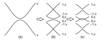
In the presence of , the mini-band structure can be obtained numerically by solving the central equation. It is found that when the potential increases the conduction mini-bands shift down and the valence mini-bands shift up, eventually the two bands cross and form a inverted band gap as shown in Fig. 1(c). Anticrossing between the two bands occurs, which is induced by the interaction term . A simple perturbative viewpoint helps us to apprehend why the periodic potential tends to induce the band inversion. Take the band () for our illustration. For a weak , the calculation up to the second order perturbation gives the energy correction for the band ()
| (4) |
here the summation excludes the band (0, c) itself, and are the unperturbated eigen state and eigen energy of the mini-band in the first BZ. Using the Fourier series of the potential, we have couples the band () and other conduction bands () stronger than the valence bands since they come from same original bands and share the same spin indices. We have . Thus we draw the conclusion that the perturbative correction is always negative, , whose effect is shifting the band () downward. Similarly, the valence band () shifts upward in the field. At a certain value of , the two bands cross and open a gap again, i.e. a negative one. Similar argument can be applied to other mini-bands. With increasing , more and more mini-bands will cross near the zero energy point. Thus the band inversion occurs consecutively because of the shifting of the mini-bands from the conduction and valence bands.
The formation of the inverted band gap is of topological and experimental interests. To gain a quantitative insight of this physical picture, we discretize the Hamiltonian in Eq. (2) on a square lattice. Without losing generality, we make the parameters material independent by setting , and the lattice space . Eigen energies and eigen states are solved numerically for the periodic system. Following Thouless and his co-workers,Thouless-82prl we come to calculate the Hall conductance of in the band gap, which is equivalent to the Chern number of the filled valence bands. The Berry curvature for each band is defined asChang-08jpcm
| (5) |
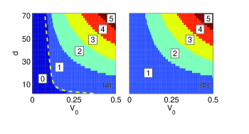
The first Chern number in the band gap is then computed by summing up Berry curvatures of the occupied bands and integrate over the first BZ The Hall conductance for is related to the first Chern number by .Thouless-82prl ; Kohmoto-85ap In the absence of the potential, the Chern number was found to be .Lu-09xxx The signs of the two model parameters in the term of determine the value of , or , and further whether the system is topologically trivial or not. In the presence of , it is found that the Chern number changes by 1 when the valence and conduction bands cross. By continually changing the potential period and potential magnitude , we obtain a phase diagram for the Chern number in Fig. 2 with the numbers in the boxes indicating the values. We see that in this system the Chern number is a function of the potential period and amplitude .
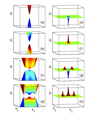
Examination of the evolution of the band structure and Berry curvature at the transition courses further confirms our claim. In Fig. 3 we show the first two transitions from to , and from to . By increasing , the band gap closes and re-opens in Fig. 3(a) and 3(b). Correspondingly, the Berry curvature peak become sharp, and reverses its value dramatically, which accounts for the change in the Chern Number. At the corresponding points, the eigen wave functions also switch their band indexes quickly. By further increasing , the peak of the Berry curvature splits into two sub-peaks, and the third peak with an opposite sign grows up while the Chern number remain to be . In the second transition, the third peaks reverses again just like the first transition, and the Chern number changes from to . Therefore accompanied by every ”closing and re-opening” of the band gap the Chern number changes by one.
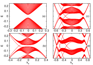
According to the edge-bulk correspondenceHatsugai-93prl ; Qi-06prb , the first Chern number determines number of the edge states when the system has an open boundary. We take a strip geometry that is parallel to the x direction with open boundary condition along the y direction. We start from a topological trivial case of and and scrutinize its changing in the band structure when varying the periodic potential . In the absence of the potential the system is insulating and topologically trivial indicated by a positive band gap. As increases, the conduction bands shift down and valence bands shift up. Eventually the two bands cross, and a band gap re-opens. A pair of edge states appears connecting the valence and conduction bands as shown in Fig. 4b. Detailed analysis shows that the wave functions of these states indeed reside on the sample edges only. As goes further up, more bands cross and more pairs of edge states are formed at distinct points as shown in Figs. 4c and 4d. It is interesting to observe that the band gap at always retains a finite value at certain stages throughout the evolution. We can see the appearance of the edge states corresponds to the change of the Chern number from to by comparing Figs. 3 and 4. Thus modulation of edge state numbers is clearly reflected in the step wise changing of the Chern numbers.
and are the time reversal counterparts of each other. Each edge state in has a couterpart in , and they form a pair of helical edge state. As a result, the large Chern number () indicates multiple pairs of helical edge states in the system in this periodic potential . For a thin film fabricated on the substrate, the top-bottom symmetry will be broken due to the interface of the thin film and the substrate. This fact will remove the degeneracy of the spectra from and . An off-diagonal term of structural inversion asymmetry is added to the model in Eq. (1),Xue-09np which connects the up and down blocks ( is the identity matrix). Similar physics happens if the sample breaks the bulk inversion symmetry in quantum well.Konig-08JPSJ In the presence of , numerical calculation still demonstrates existence of the edge states in the four-band model, which is characteristic of QSH phase. Thus this term does not destroy the QSH phase explicitly.
Feasibility of experimental realization of this phenomenon depends on spin decoherence length in the sample, and the fabrication of the periodic potential. The spin decoherence length was estimated to be in the HgTe/CdTe quantum well,Konig-07science ; Roth-09science and expected to be longer in a thin film of Bi2Se3.Xue-09np On the periodicity of the modulated electric field, the sub-100nm period of SSL fabrications was reported a decade ago,Messica-97prl and the 3nm periodicity for a graphene on Ru(111) recently.Marchini-07prb For a set of realistic parameters for HgTe/CdTe quantum well with a normal band gap meV,Bernevig-06science the magnitude of the potential with periodicity nm is calculated to meV for the transition of to and meV for the transition of to . We speculate that the modern techniques of superlattice make this electric field modulation possible.
In summary, the band structure of a thin film or quantum well are folded into the mini-bands in the reduced BZ by a periodic potential, and can be modulated such that the conduction bands shift downward and the valence bands shift upward. Each process of the band gap closing and re-opening will change the Chern number by one. As a result the number of the helical edge states will increase or decrease by one. This demonstrates the possibility of the electric field modulation of topological orders in the thin film semiconductors, which is analogous to the integer quantum Hall effect in a strong magnetic field. Direction of electrons of the helical edge states is of interests in quantum information and quantum processing. Controllable number of the helical edge states will pave an alternative route for application of edge state physics in the future.
This work was supported by the Research Grant Council of Hong Kong under grant No.: HKU 704107 and HKU 10/CRF/08.
∗These authors contributed equally to this work.
†E-mail: sshen@hkucc.hku.hk
References
- (1) For introductions to topological insulators, see S. C. Zhang, Physics 1, 6 (2008); M. Buttiker, Science 325, 278 (2009); J. Moore, Nature Physics 5, 378 (2009).
- (2) C. L. Kane and E. J. Mele, Phys. Rev. Lett. 95, 226801 (2005)
- (3) B. A. Bernevig, T. L. Hughes, and S. C. Zhang, Science 314, 1757 (2006).
- (4) M. König, S. Wiedmann, C. Brüne, A. Roth, H. Buhmann, L. W. Molenkamp, X. L. Qi, and S. C. Zhang, Science 318, 766 (2007).
- (5) Liang Fu, C. L. Kane, and E. J. Mele, Phys. Rev. Lett. 98, 106803 (2007).
- (6) D. Hsieh, D. Qian, L. Wray, Y. Xia, Y. S. Hor, R. J. Cava and M. Z. Hasan, Nature 452, 970 (2008).
- (7) Y. Xia, D. Qian, D. Hsieh, L. Wray, A. Pal, H. Lin, A. Bansil, D. Grauer, Y. S. Hor, R. J. Cava and M. Z. Hasan, Nature Physics 5, 398 (2009).
- (8) H. Zhang, C. X. Liu, X. L. Qi, X. Dai, Z. Fang, and S. C. Zhang, Nature phys. 5, 438 (2009).
- (9) Y. L. Chen, J. G. Analytis, J.-H. Chu, Z. K. Liu, S.-K. Mo, X. L. Qi, H. J. Zhang, D. H. Lu, X. Dai, Z. Fang, S. C. Zhang, I. R. Fisher, Z. Hussain, and Z.-X. Shen, Science 325, 178 (2009).
- (10) C. L. Kane and E. J. Mele, Phys. Rev. Lett. 95, 146802 (2005)
- (11) J. E. Moore and L. Balents, Phys. Rev. B 75 121306 (2007)
- (12) A. Shitade, H. Katsura, J. Kuneš, X. L. Qi, S. C. Zhang, and N. Nagaosa, Phys. Rev. Lett. 102, 256403 (2009).
- (13) A. Roth, C. Brune, H. Buhmann, L. W. Molenkamp, J. Maciejko, X. L. Qi, S. C. Zhang, Science 325, 294 (2009)
- (14) R. Tsu, Superlattice to Nanoelectronics (Elsevier, Oxford, 2005).
- (15) H. Z. Lu, W. Y. Shan, W. Yao, Q. Niu, and S. Q. Shen, arXiv: 0908.3120.
- (16) R. Winkler, Spin-orbit Coupling Effects in Two-Dimensional Electron and Hole Systems, p. 64, (Springer, Berlin, 2003).
- (17) C. Kittel, Introduction to Solid State Physics (7th ed.), Chap. 7, p. 183, (John Wiley & Sons, New York, 1996)
- (18) D. J. Thouless, M. Kohmoto, M. P. Nightingale, and M, deb Nijs, Phys. Rev. Lett. 49, 405 (1982).
- (19) M. C. Chang and Q. Niu, J. Phys.: Cond. Mat. 20, 193202 (2008); D. Xiao, M. C. Chang and Q. Niu, arXiv: 0907.2021
- (20) M. Kohmoto, Ann. Phys. (NY) 160, 343 (1985).
- (21) Y. Hatsugai, Phys. Rev. Lett. 71, 3697 (1993).
- (22) X. L. Qi, Y. S. Wu, and S. C. Zhang, Phys. Rev. B 74 045125 (2006)
- (23) Y. Zhang et al, preprint submitted to Nature Phsyics, (2009); W. Y. Shan et al, in preparation.
- (24) M. König, H. Buhmann, L. W. Molenkamp, T. Hughes, C. X. Liu, X. L. Qi, and S. C. Zhang, J. Phys. Soc. Jpn. 77, 031007 (2008).
- (25) A. Messica, A. Soibel, U. Meirav, A. Stern, H. Shtrikman, V. Umansky, and D. Mahalu, Phys. Rev. Lett. 78, 705 (1997).
- (26) S. Marchini, S. Gunther, and J. Wintterlin, Phys. Rev. B 76, 075429 (2007)