Features due to spin-orbit coupling in the optical conductivity of single-layer graphene
Abstract
We have calculated the optical conductivity of a disorder-free single graphene sheet in the presence of spin-orbit coupling, using the Kubo formalism. Both intrinsic and structural-inversion-asymmetry induced types of spin splitting are considered within a low-energy continuum theory. Analytical results are obtained that allow us to identify distinct features arising from spin-orbit couplings. We point out how optical-conductivity measurements could offer a way to determine the strengths of spin splitting due to various origins in graphene.
pacs:
81.05.Uw, 72.10.Bg, 71.70.EjI Introduction
Graphene is a single sheet of carbon atoms forming a two-dimensional honeycomb lattice. This material has only recently become available for experimental study, and its exotic physical properties have spurred a lot of interest novoselov2004 ; novoselov2005 . Known theoretically since the late 40s wallace1947 , graphene is a promising candidate for applications due to its excellent mechanical properties lee2008 , scalability down to nanometer sizes scalability , and exceptional electronic properties castroneto2009 . The conical shape of conduction and valence bands near the and points in the Brillouin zone renders graphene an interesting type of quasi-relativistic condensed-matter system zhang2005 ; novoselov2005_2 where mass-less Dirac-fermion-like quasiparticles are present at low energy. In contrast to the truly relativistic case, the spin degree of freedom in their Dirac equation corresponds to a pseudo-spin that distinguishes degenerate states on two sublattices formed by two nonequivalent atom sites present in the unit cell.
The pseudo-spin degeneracy can be broken by spin-orbit interaction (SOI), which mixes pseudospin and real spin. There has been huge interest in SOI in graphene, resulting in a large body of theoretical dressel ; ando2000 ; egger ; mele_kane2005 ; huertas-hernando2006 ; min2006 ; yao2007 ; boettger2007 ; zarea ; guinea2 ; guinea3 ; rashba2009 ; fabian2009 ; stauber2009 ; kuemmeth2009 ; gmitra2009 and experimental kuemmeth2008 ; laubschat2008 ; varykhalov2008 ; rader2009 ; varykhalov2009 work. There are two main causes for the SOI in graphene. Firstly, external electric fields (e.g., due to the presence of a substrate, a backgate, or adatoms) and local curvature fields (ripples) induce a SOI mele_kane2005 ; huertas-hernando2006 ; min2006 ; rashba2009 ; gmitra2009 whose coupling strength we denote by . We refer to this contribution as the Rashba SOI in the following. In addition, there is an intrinsic SOI dressel ; mele_kane2005 ; huertas-hernando2006 ; min2006 ; yao2007 ; boettger2007 ; gmitra2009 with strength , which is caused by the atomic Coulomb potentials.
Existence of the intrinsic and Rashba SOIs can be inferred from group-theoretical arguments dressel ; mele_kane2005 ; rashba2009 . However, the actual values of their respective strengths and are the subject of recent debate. Initial estimates mele_kane2005 have been refined using tight-binding models huertas-hernando2006 ; min2006 and density-functional calculations yao2007 ; boettger2007 ; gmitra2009 . First experimental observations of spin-orbit-related effects in graphene’s band structure based on ARPES data laubschat2008 ; varykhalov2008 have later been questioned rader2009 ; varykhalov2009 . Detailed knowledge about typical magnitudes and ways to influence and is crucial, e.g., for understanding spin-dependent transport wees2007 and spin-based quantum devices trauzettel2007 in graphene. The desire to identify possible alternative means of observing, and measuring, spin-orbit coupling strengths in graphene has provided the motivation for our work reported here.
We present a theoretical analysis of graphene’s optical conductivity , extending previous studies ziegler2006 ; gusynin2006 ; ziegler2007 ; falkovsky2007 ; peres2008 ; nicol2008 ; zhang2008a ; gusynin2009 ; uz:physe:10 to the situation with finite SOI. SOI effects on the DC conductivity were investigated in a recent theoretical study for a bipolar graphene junction yamakage2009 , and the effect of intrinsic SOI on the polarisation-dependent optical absorption of graphene was considered in Ref. zhang2008b, . Our study presents the analogous scenario for the richer case of the optical conductivity when both intrinsic and extrinsic types of SOI are present. Since can be tuned by external fields, we will analyze various situations distinguished by the relative strengths of and .
Our findings suggest that optical-conductivity measurements can be useful to identify and separate different SOI sources. We work on the simplest theory level (linear response theory, no interactions, no disorder) and disregard boundary effects for the moment. The structure of the remainder of this article is as follows. In Sec. II, we summarize basics of our calculation of the optical conductivity based on the Kubo formalism; except for some details that have been relegated to an Appendix. In Sec. III, we show results for different relative magnitudes of SOI strengths at finite temperature and chemical potential . Finally, in Sec. IV, we summarize our results and discuss their applicability to actual experiments.
II Optical conductivity
We start from a low-energy continuum description of graphene castroneto2009 , Without the SOI terms and , the single-particle Hamiltonian in plane-wave representation reads
| (1) |
with Fermi velocity m/s. The Pauli matrices act in pseudo-spin space, where the two eigenspinors of correspond to quasiparticle states localized on sites of the and sublattice. Analogous Pauli matrices act in the two-valley space spanned by states near the two points. The part of the effective Hamiltonian describing Rashba SOI is given by
| (2) |
where includes both the external electric-field and curvature effects in a coarse-grained approximation, with the latter assumed to be homogeneous. The Pauli matrices act in the real spin space. For the intrinsic SOI induced by atomic potentials, we have
| (3) |
The full Hamiltonian is then an matrix in the combined sublattice, spin, and valley space.
The full Hamiltonian matrix turns out to be block-diagonal in the valley degree of freedom, and each block can be transformed into the other via a unitary transformation. The bulk spectrum – ignoring subtleties related to the topological insulator phase encountered for mele_kane2005 for now – can then be obtained from a Hamiltonian matrix in the basis at one point. The valley degree of freedom then merely manifests itself as a degeneracy factor . The energy spectrum is obtained as
| (4) |
where the combined indices label the four bands. The corresponding eigenstates
| (5) |
are composed of a plane wave state and a -dependent 4-spinor .
We compute the optical conductivity using the standard Kubo formula mandelung ,
| (6) |
where and the kernel reads
| (7) |
Here denotes the electron charge, is a Cartesian component of the position operator, the equilibrium density matrix, and the current operators are given by
| (8) |
Following Ref. ziegler2006, , we use the single-particle eigenstates and eigenenergies . The conductivity then reads
| (9) | |||||
where is the Fermi-Dirac distribution containing the chemical potential and the inverse temperature .
In the absence of a magnetic field, the off-diagonal entries vanish, , while symmetry arguments show that . At finite in the clean system, only the inter-band contribution to the conductivity is relevant. Its real part is given by
| (10) | |||
where
are the current operator matrix elements in the eigenbasis, and . We also used
since the current operator is Hermitian. In what follows, we restrict ourselves to the real part of and omit the “Re” sign.
The result obtained for can be expressed very generally as
| (11) |
where and, with the Heaviside function , the quantities are given by
| (12) |
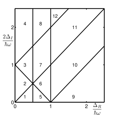
The rather lengthy analytical expressions for the quantities can be found in the Appendix. In Fig. 1, we show the regions in the -plane where the different contribute.
| 1-3, 5-7, 10, 11 | 6-8 | 1-3, 5-7, 9-11 | 1, 2 | 10-12 | 1, 2, 5 |
III Results
We now discuss the main physical observations arising from Eqs. (11) and (12). First, the behavior of the conductivity is qualitatively different in the two regimes and . It is well-known that the latter regime corresponds to a topological insulator phase while the former yields a conventional band insulator, with a quantum phase transition in between. For the topological insulator phase mele_kane2005 ; kane2005_2 ; brey2006 ; bernevig2006 , spin-polarized gapless edge states forming a helical liquid will dominate the optical conductivity when both and are smaller than the gap energy. In that regime, the conductivity is expected mele_kane2005 to exhibit power-law behavior analogous to that found for ordinary one-dimensional electron systems giamarchi1988 ; giamarchi1992 . In what follows, we consider the frequency and temperature range such that the optical conductivity is still mostly determined by the bulk states.
Sharp features are exhibited by the conductivity as a function of frequency , which depend on the relative strength of the two SOI terms and should therefore allow for a clear identification of these couplings. We start by discussing a few special cases. For but finite , the gapped spectrum consisting of two doubly (spin-)degenerate dispersion branches leads to a vanishing conductivity for , and all other features expected in the presence of a generic mass gap gusynin2006 ; gusynin2009 . In contrast, for but finite , the band structure mimics that of bilayer graphene, only with a gap smaller by up to 4 orders of magnitude dressel ; mcclure1957 . The optical conductivity for this case has the same functional form as the conductivity for bilayer graphene nicol2008 ; uz:physe:10 , except that the McClure mcclure1957 interlayer hopping constant is replaced by . In particular, it exhibits a -peak at and a kink at . With , the analytical expression is
| (13) | |||
where we define the function
| (14) |
In the limit , the optical conductivity of clean graphene with its spin-degenerate linear dispersion is recovered ziegler2007 ; falkovsky2007 . The asymptotic behavior for large frequencies turns out to be independent of the SOI couplings, with always approaching the well-known universal value .
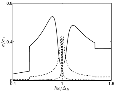
The optical conductivity for various situations where both and are finite is shown next in a series of figures. In particular, Fig. 2 shows the case where . In Fig. 3, we are at the special point . Furthermore, Fig. 4 illustrates the regime where . To be specific, all these figures are for K. Finally, Fig. 5 displays the effects of thermal smearing.
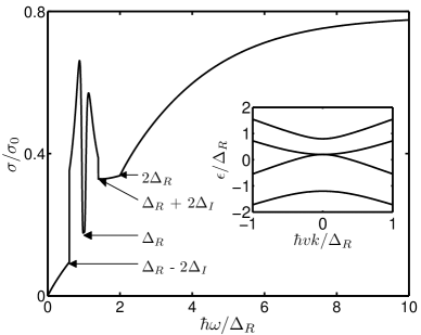
For , we observe a splitting and widening of the -peak at , while the kink at stays at the same position. In addition, we observe kinks at , see Fig. 2.
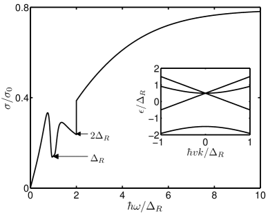
At the quantum phase transition point , the dispersion exhibits a crossing of two massless branches with a massive branch, see inset of Fig. 3. As a consequence, certain sharp features exhibited by the optical conductivity in other cases disappear .
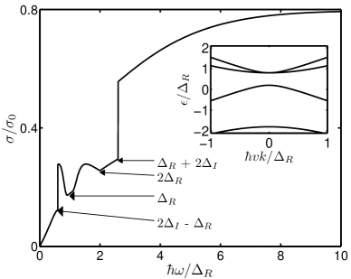
For , see Fig. 4, the conductivity shows kinks at , at , and at .
We have chosen to show a very wide range of SOI parameters and in these figures. Previous estimates for these parameters mele_kane2005 ; min2006 ; huertas-hernando2006 ; yao2007 ; boettger2007 ; gmitra2009 range from 0.5 eV to 100 eV for , and 0.04 eV to 23 eV for . The Rashba coupling is expected to be linear in the electric backgate field, with proportionality constant 10 eV nm/V (Ref. gmitra2009, ), allowing for an experimental lever to sweep through a wide parameter range. On the experimental side, the picture is currently mixed. One recent experimental study kuemmeth2008 finds eV (eV) for electrons (holes) in carbon nanotubes. A much larger value meV has been reported for graphene sheets fabricated on a nickel surface varykhalov2008 .
For low temperatures (e.g., at K in the above figures), the SOI couplings can be distinguished by the different peak structures appearing in the optical conductivity. Increasing the temperature leads to thermal smearing of those features, as illustrated in Fig. 5. However, the characteristic SOI-induced peak and kink features should still be visible in the optical conductivity up to K, albeit with a smaller magnitude.
IV Conclusions
We have calculated the optical conductivity for a graphene monolayer including the two most relevant spin-orbit couplings, namely the intrinsic atomic contribution and the curvature- and electric-field-induced Rashba term . Our result for the optical conductivity, which we presented for finite temperature and chemical potential, shows kinks and/or peaks at frequencies corresponding to , , and . Measuring the optical conductivity in a frequency range covering these energy scales can be expected to yield detailed insights into the nature of spin-orbit interactions in graphene.
We did not analyze disorder effects but expect all sharp features to broaden since the -functions in Eq. (II) effectively become Lorentzian peaks. We also did not consider the effect of electron-electron interactions. While renormalization group studies indicate that weak unscreened interactions are marginally irrelevant castroneto2009 , interactions may still play an important role. For instance, Ref. grushin2009, considers interaction effects on the optical properties of doped graphene without spin-orbit coupling. Interactions cause inter-band (optical) and intra-band (Drude) transitions and thus a finite DC conductivity. We expect that the peak and kink structures arising from the spin-orbit couplings survive, however, because the relevant contributions are additive.
Recent experimental studies suggest that an optical measurement of the conductivity in the energy range relevant for SOI should be possible. Fei et al. fei2008 have measured the optical conductivity from eV up to eV. Slightly lower energies ( eV to eV) were reached in Ref. mak2008, . We suggest to perform low-temperature experiments at microwave frequencies, with energies ranging from several eV to a few meV.
Acknowledgements.
Useful discussions with M. Jääskeläinen are gratefully acknowledged. JZB is supported by a postdoctoral fellowship from the Massey University Research Fund. Additional funding was provided by the German Science Foundation (DFG) through SFB Transregio 12.Appendix A Definition of auxiliary functions
Here we provide the six functions (with ) entering Eq. (12). We use the following abbreviations:
Furthermore, we define the quantities (setting here for simplicity)
Finally, we define . With these conventions, the functions can be expressed as follows:
References
- (1) K. S. Novoselov, A. K. Geim, S. V. Morozov, D. Jiang, Y. Zhang, S. V. Dubonos, I. V. Grigorieva, and A. A. Firsov, Science 306, 666 (2004).
- (2) K. S. Novoselov, D. Jiang, F. Schedin, T.J. Booth, V. V. Khotkevich, S. V. Morosov, and A. K. Geim, PNAS 102, 10451 (2005).
- (3) P. R. Wallace, Phys. Rev. 71, 622 (1947).
- (4) C. Lee, X. Wei, J. W. Kysar, and J. Hone, Science 321, 5887 (2008).
- (5) P. Avouris, Z. Chen, and V. Perebeinos, Nat. Nanotech. 2, 605 (2007); Z. Chen, Y.-M. Lin, M. J. Rooks, and P. Avouris, Physica E 40, 228 (2007); J. B. Oostinga, H. B. Heersche, X. Liu, A. F. Morpurgo, and L. M. K. Vandersypen, Nat. Mater. 7, 151 (2007).
- (6) A. H. Castro Neto, F. Guinea, N. M. R. Peres, K. S. Novoselov, and A. K. Geim, Rev. Mod. Phys. 81, 109 (2009).
- (7) Y. Zhang, Y. Tan, H. L. Stormer, and P. Kim, Nature (London) 438, 201 (2005).
- (8) K. S. Novoselov, A. K. Geim, S. V. Morozov, D. Jiang, Y. Zhang, S. V. Dubonos, I. V. Grigorieva, and A. A. Firsov, Nature (London) 438, 197 (2005).
- (9) G. Dresselhaus and M. S. Dresselhaus, Phys. Rev. 140, 401 (1965).
- (10) T. Ando, J. Phys. Soc. Jpn. 69, 1757 (2000).
- (11) A. De Martino, R. Egger, K. Hallberg, and C. A. Balseiro, Phys. Rev. Lett. 88, 206402 (2002).
- (12) C. L. Kane and E. J. Mele, Phys. Rev. Lett. 95 226801 (2005).
- (13) D. Huertas-Hernando, F. Guinea, and A. Brataas, Phys. Rev. B 74, 155426 (2006).
- (14) H. Min, J. E. Hill, N. A. Sinitsyn, B. R. Sahu, L. Kleinman, and A. H. MacDonald, Phys. Rev. B. 74, 165310 (2006).
- (15) Y. Yao, F. Ye, X. L. Qi, S. C. Zhang, and Z. Fang, Phys. Rev. B 75 041401(R) (2007).
- (16) J. C. Boettger and S. B. Trickey, Phys. Rev. B 75, 121402(R) (2007).
- (17) M. Zarea and N. Sandler, Phys. Rev. B 79, 165442 (2009).
- (18) D. Huertas-Hernando, F. Guinea, and A. Brataas, Phys. Rev. Lett. 103, 146801 (2009).
- (19) A. H. Castro Neto and F. Guinea, Phys. Rev. Lett. 103, 026804 (2009).
- (20) E. I. Rashba, Phys. Rev. B 79, 161409(R) (2009).
- (21) C. Ertler, S. Konschuh, M. Gmitra, and J. Fabian, Phys. Rev. B 80, 041405(R) (2009).
- (22) T. Stauber and J. Schliemann, New. J. Phys. 11, 115003 (2009).
- (23) F. Kuemmeth and E. I. Rashba, Phys. Rev. B 80, 241409(R) (2009).
- (24) M. Gmitra, S. Konschuh, C. Ertler, C. Ambrosch-Draxl, and J. Fabian, arXiv:0904.3315 (unpublished).
- (25) F. Kuemmeth, S. Ilani, D. C. Ralph, and P. L McEuen, Nature (London) 452, 448 (2008).
- (26) Yu. S. Dedkov, M. Fonin, U. Rüdiger, and C. Laubschat, Phys. Rev. Lett. 100, 107602 (2008).
- (27) A. Varykhalov, J. Sanchez-Barriga, A. M. Shikin, C. Biswas, E. Vescovo, A. Rybkin, D. Marchenko, and O. Rader, Phys. Rev. Lett. 101, 157601 (2008).
- (28) O. Rader, A. Varykhalov, J. Snachez-Barriga, D. Machenko, A. Rybkin, and A. M.Shikin, Phys. Rev. Lett. 102, 057602 (2009).
- (29) A. Varykhalov and O. Rader, Phys. Rev. B 80, 035437 (2009).
- (30) N. Tombros, C. Jozsa, M. Popinciuc, H. T. Jonkman, and B. J. van Wees, Nature (London) 448, 571 (2007).
- (31) B. Trauzettel, D. V. Bulaev, D. Loss and G. Burkard, Nat. Phys. 3, 192 (2007).
- (32) K. Ziegler, Phys. Rev. Lett. 97, 266802 (2006).
- (33) V. P. Gusynin, S. G. Sharapov, and J. P. Carbotte, Phys. Rev. Lett. 96, 256802 (2006).
- (34) K. Ziegler, Phys. Rev. B 75, 233407 (2007).
- (35) L. A. Falkovsky and A. A. Varlamov, Eur. Phys. J. B 56, 281 (2007).
- (36) N. M. R. Peres, T. Stauber, and A. H. Castro Neto, Europhys. Lett. 84 38002, (2008).
- (37) E. J. Nicol and J. P. Carbotte, Phys. Rev. B 77, 155409 (2008)
- (38) C. Zhang, L. Chen, and Z. Ma, Phys. Rev. B 77, 241402(R) (2008).
- (39) V. P. Gusynin, S. G. Sharapov, and J. P. Carbotte, New. J. Phys. 11, 095013 (2009).
- (40) J. Z. Bernád, U. Zülicke, and K. Ziegler, Physica E, in press (doi:10.1016/j.physe.2009.11.076).
- (41) A. Yamakage, K.-I. Imura, J. Cayssol, and Y. Kuramoto, Europhys. Lett. 87, 47005 (2009).
- (42) A. R. Wright, G. X. Wang, W. Xuc, Z. Zeng, and C. Zhang, Microelec. J. 40, 857 (2009).
- (43) O. Madelung, Introduction to Solid-State Theory (Springer, Berlin, 1978).
- (44) C. L. Kane and E. J. Mele, Phys. Rev. Lett. 95, 146802 (2005).
- (45) L. Brey and H.A. Fertig, Phys. Rev. B 73, 195408 (2006).
- (46) C. Wu, B. A. Bernevig, and S.-C. Zhang, Phys. Rev. Lett. 96, 106401 (2006).
- (47) T. Giamarchi and H. Schulz, Phys. Rev. B 37, 325 (1988).
- (48) T. Giamarchi and A. J. Millis, Phys. Rev. B 46, 9325 (1992).
- (49) J. W. McClure, Phys. Rev. 108, 612 (1957).
- (50) A. G. Grushin, B. Valenzuela, and M. A. H. Vozmediano, Phys. Rev. B 80, 155417 (2009).
- (51) Z. Fei, Y. Shi, L. Pu, F. Gao, Y. Liu, L. Sheng, B. Wang, R. Zhang, and Y. Zheng, Phys. Rev. B 78, 201402(R) (2008).
- (52) K. F. Mak, M. Y. Sfeir, Y. Wu, C. H. Lui, J. A. Misewich, and T. F. Heinz, Phys. Rev. Lett. 101, 196405 (2008).