11email: rhijmeri@rssd.esa.int 22institutetext: Cambridge MicroFab Ltd., Broadway, Bourn, Cambridgeshire CB3 7TA, UK 33institutetext: Department of Astrophysics, Radboud University Nijmegen, P.O. Box 9010, 6500 GL Nijmegen, The Netherlands
First results of a cryogenic optical photon counting imaging spectrometer using a DROID array
Abstract
Context. In this paper we present the first system test in which we demonstrate the concept of using an array of Distributed Read Out Imaging Devices (DROIDs) for optical photon detection.
Aims. After the successful S-Cam 3 detector the next step in the development of a cryogenic optical photon counting imaging spectrometer under the S-Cam project is to increase the field of view using DROIDs. With this modification the field of view of the camera has been increased by a factor of 5 in area, while keeping the number of readout channels the same.
Methods. The test has been performed using the flexible S-Cam 3 system and exchanging the 10x12 Superconducting Tunnel Junction array for a 3x20 DROID array. The extra data reduction needed with DROIDs is performed offline.
Results. We show that, although the responsivity (number of tunnelled quasiparticles per unit of absorbed photon energy, e-/eV) of the current array is too low for direct astronomical applications, the imaging quality is already good enough for pattern detection, and will improve further with increasing responsivity.
Conclusions. The obtained knowledge can be used to optimise the system for the use of DROIDs.
Key Words.:
detectors:photometers: spectographs: spectrometer1 Introduction
With the S-Cam project the Advanced Studies & Technology Preparation Division of the European Space Agency is developing a series of prototype cryogenic detectors to be used as optical photon counting imaging spectrometers for ground-based astronomy. S-Cam uses Superconducting Tunnel Junctions (STJs) (Friedrich et al. (2006); Prober et al. (2006); Peacock et al. (1996)) as its detector technology. The merit of this and other cryogenic detectors (Romani et al. (1999)) is that they combine single photon detection with sub-microsecond time resolution and intrinsic wavelength resolution, imaging and good detection efficiency in a single device.
STJs consist of 2 superconducting layers separated by a thin insulating layer acting as a tunnel barrier. With the absorption of a photon in the superconducting layer a large quantity (several thousands) of Cooper pairs are broken into quasiparticles which can tunnel across the barrier and, under the influence of an applied bias voltage, produce a measurable current pulse. The number of created quasiparticles is given by: , with the number of created quasiparticles, the energy of the absorbed photon and the mean energy needed to create a quasiparticle (Kurakado et al. (1981)) with the energy gap of the superconducting material. As shown the number of created quasiparticles, and hence the amplitude of corresponding tunnel current, is proportional to the energy of the absorbed photon, thus providing the detector with its spectrographic capabilities. The theoretical limit for the intrinsic energy resolution is given by: , where is the Fano factor (Fano (1947)), equal to (Kurakado et al. (1981); Rando et al. (1991)), and (Mears et al. (1993)) accounts for the statistical variations in the tunnel process, with the average number of tunnels of a single quasiparticle. The energy gap, , of the superconducting material is proportional to its critical temperature, ), the temperature at which the phase changes from superconducting to normal metal. For a BCS type superconductor (usually an elemental superconducting material which follows the theory developed by Bardeen et al. (1957)), . A lower energy gap of the superconducting material will therefore increase the number of created quasiparticles and provide better spectrographic capabilities, but it also puts increasing constraints on the operating temperature (). This needs to be well below the critical temperature of the superconducting layer () in order to sufficiently reduce the thermally excited quasiparticle population. For a more extended overview of the STJ technology the reader is referred to Peacock et al. (1996).
Each STJ needs to be read out using a dedicated electronics chain which limits the maximum number of pixels that can be read out in a practical application (Martin et al. (2006)). To overcome this limitation the Distributed Read Out Imaging Device (DROID) (Kraus et al. (1989)) is being developed. A DROID consists of a superconducting absorber strip with STJs on either end, see fig. 1. The photon is absorbed in the absorber and the created quasiparticles diffuse towards the STJs where they tunnel. The sum of the tunnel signals of both STJs is a measure for the energy of the absorbed photon while the ratio is a measure for the absorption position. Depending on the position resolution of the DROID it can replace a number of single STJs and reduce the number of read out channels for a given sensitive area (Hijmering et al. (2008)).
Within the S-Cam project three prototype cameras have already successfully been used on telescopes such as the William Herschel Telescope (WHT) on La Palma and the Optical Ground Station (OGS) on Tenerife (Martin et al. (2004)). S-Cam 1 (Verhoeve et al. (2002)) and 2 (Rando et al. (2000)) were based on a pixel array ( pixels) with a wavelength resolving power of 6. S-Cam 3 (Martin (2007); Martin et al. (2006)) was based on a pixel array ( pixels), increasing the field of view on the WHT from to . Also the covered wavelength range, operating temperature and resolving power () has been enhanced with S-Cam 3. The applicability of this type of detector has been proven in different observation campaigns in which several types of astronomical objects have been observed. The high time resolution spectrally resolved S-Cam data has provided strong constraints on the geometry of eclipsing binaries (Perryman et al. (2001); de Bruijne et al. (2002); Martin et al. (2003)). Precise timing of the Crab pulsar light curve has shown that the optical pulses lead the radio pulses by (Perryman et al. (1999); Oosterbroek et al. (2006)). The spectral information provided by the STJs has enabled the direct determination of quasar redshifts (de Bruijne et al. (2002)) and stellar temperatures (Reynolds et al. (2003)). The next step is to increase the field of view further with the use of DROIDs. Here we present the results of the first system test using a DROID array as a detector.
2 Operation of the DROID array
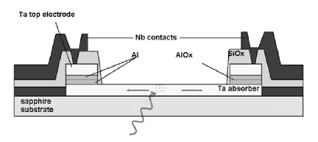
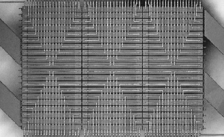
The DROID array, shown in fig. 2, is fabricated by MicroFab Ltd. and is based on pure tantalum absorbers () with proximized Ta/Al STJs on the side (). The lay-up of the STJs is Ta/Al/AlOx/Al/Ta with thicknesses of 100/30/1/30/100. The 100 thick tantalum absorber of the DROID and the tantalum layer of the base electrode of the STJ (see fig. 1) are made of a single layer of tantalum. The presence of the aluminium layer in the STJ reduces the energy gap due to the proximity effect (Booth (1987)) and provides confinement of quasiparticles inside the STJ, which enhances the performance. The confinement of quasiparticles using this method is not always 100% effective and quasiparticles which reside at higher energies, , are able to escape the STJ into the absorber. The DROIDs are in size, including the STJs. The DROIDs are separated by wide gaps to accommodate the interconnections between the base electrodes of the STJs, which share a common return wire. These interconnections are made of higher gap material (Nb, ) which prevents diffusion of quasiparticle across the interconnections, and thereby cross talk between DROIDs. The leads to the top electrodes of the STJs are routed over the front side of the DROIDs outwards. In order to electrically isolate the leads to the top electrodes from the rest of the DROID structure the complete array has been covered with . The array is divided into 4 electrically isolated groups of DROIDs, each with a single common return lead. The devices are made on a transparent sapphire substrate which allows for backside illumination, through the sapphire. In this way the wiring routed over the absorber at the front side does not block any photons.
The individual DROIDs on the array have been characterised in a sorption refrigerator in which two DROIDs can be read out at a time. In this cryostat the devices are effectively shielded from IR radiation using a closed shield surrounding the sample space and the chip can only be illuminated via an optical fibre. The devices are biased using a small voltage bias and the electronics used to read out a single DROID at a time consist of two charge sensitive preamplifiers, with a RC time of , each followed by a shaping stage. The two channels are linked in the sense that coincident events, defined as events in either STJ, resulting from a photon absorption in the DROID which occur within (the time window is defined by the electronics and the time of arrival is defined as the time the signal passes through a threshold), can be identified and selected, while uncorrelated events are rejected. This efficiently reduces the noise-induced events as well. The resulting data for each event consists of the pulse height values of the two channels and the relative time of detection.

The characterisation of the array showed that two DROIDs in the array were erroneously interconnected and one DROID showed increased subgap current levels. Fig. 3a and b shows the relative pulse height (sum of the two STJ pulse heights) and wavelength resolving power , respectively, of the DROIDs in the array as a function of position along the absorber (derived from the ratio of the two STJ pulse heights) under illumination with photons. The relative responsivity and resolving power of the DROIDs are determined by fitting a Gaussian to the resulting single peak in pulse height histogram. The results show that the responsivity is rather low, roughly a order of magnitude lower compared to previously tested DROIDs. The responsivity across the array is rather non-uniform, with a standard deviation of 24%. This problem is related to the variable quality of the Nb interconnections between the base electrodes and solutions are currently under investigation. For practical use the absorber is divided into sections or virtual pixels. For S-Cam the size of a virtual pixel will be , equal to the width of the absorber, and corresponding to the seeing on the sky at the William Herschel Telescope and the Optical Ground Station. The average wavelength resolving power for the absorber events is ), and corresponds to an average position resolution of (Jochum et al. (1993); Hijmering et al. (2008)), well matched to the size of a virtual pixel. The variation in wavelength resolving power over the array is 16% (see fig. 3b) and is directly correlated to the variations in responsivity.
3 Full array test set-up
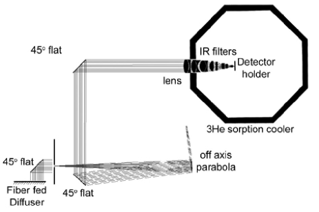
A full array test has been performed with the S-Cam 3 system (Martin et al. (2006); Martin (2007)) in which the complete array can be read out simultaneously and the array can be illuminated from the outside through a window. The optical chain, fig. 4, consists of an off axis paraboloidal mirror, two flat mirrors to fold the beam, a high quality lens system to focus the beam on the detector and a set of 3 cold IR filters (inside the cryostat) to reduce the thermal load and IR background. The optical chain has a demagnification factor of 5.4 and the available wavelength band, limited by the IR filters, is . For laboratory tests the focal plane of the off axis paraboloidal mirror is illuminated, through a diffuser, with monochromatic light from a Xe lamp and grating monochromator through a UV-grade optical fibre. A pinhole can be moved into the focal plane to project spots of various size and shapes onto the chip. The chip is back-illuminated through the sapphire substrate to avoid obscuration by the readout leads and to exploit the infrared absorption properties of sapphire. The cryostat contains a liquid helium bath and uses a double stage closed cycle evaporation cooler with a base temperature of and a hold time of hours. The readout, which is similar to the one used with the measurements on one individual DROID, is performed using 120 charge sensitive preamplifiers grouped into the four electrically isolated groups, followed by analogue-to-digital converters and a programmable Finite Impulse Response (FIR) filter which acts as a shaping stage. The implemented filters produce a bipolar output pulse for each detected photon, of which both the positive and negative peak are sampled for offline evaluation and the pass through zero of the bipolar signal defines the time of arrival with a known offset. The ratio of positive and negative peak amplitude carries information on the original pulse shape and can be used to discriminate photon induced events from other disturbances. Each event in the STJ is labeled with a accurate time stamp derived from a GPS (Global Positioning System) signal. The collected data for each detected event consists of the label of the STJ, the pulse height values for the positive and negative amplitudes and a time stamp.
Although the data acquisition system is very flexible it is currently geared towards the readout of an array of 120 single STJs, which introduces some complications for the read out of DROIDs. The signal in one of the STJs of a DROID decreases with distance between the absorption position and the STJ, and in order to detect the signals from absorptions near the far side STJ the thresholds for the individual channels need to be set sufficiently low, which introduces a large amount of noise-induced events. Identification and selection of coincident events in the two STJs of a DROID cannot be performed at a hardware level yet and therefore all triggered events (including noise triggers) have to be recorded. Coincident event selection is then performed offline using the time stamps of the individual events. Implementation of the DROID array and operation of the system proved to be not more difficult than the operation of the original 120 pixel S-Cam 3 detector array. Similar to previous experience, the array was more sensitive to the trapping of magnetic flux due to the larger superconducting area of the chip and multiple cool down cycles were required before an optimally functioning array was obtained. During the measurement four DROIDs where set inactive to allow stable operation: the two interconnected DROIDs, the DROID with increased subgap current levels and one DROID which remained flux trapped. Flux trapping can be removed by heating up the devices to a temperature above , removing any remnant field and cool down. If the magnetic field is low enough no flux will be trapped. For future use the interconnected DROIDs can be separated and improved magnetic shielding should remove the flux trapping entirely leaving only a single bad DROID in the array. Because of the low responsivity of the DROID array only the shortest wavelengths in the available wavelength band could be used for illumination. Even so, the signal for some of the DROIDs did not reach above the detection threshold. For the current demonstration this results effectively in a non-uniform efficiency, which can be reduced using a flat field correction. However, because of the low responsivity the array is not useful for application on a telescope.
4 Data reduction
Despite the non-uniformity, the data of the DROIDs in the array shows fairly similar patterns and the off-line data reduction can easily be automated. The individual event data are initially filtered on the ratio of the positive and negative peak amplitudes (fig. 5a) which should be close to unity for true photon absorptions (Martin (2007)). Coincident events are defined as events in the two STJs belonging to the same DROID which occur within , this time window is set manually in the offline data reduction and is optimized for the obtained data. In this step of the events, mainly noise-induced events, are filtered out making it the most important filtering step. Even with current computational power it takes several hours to complete this filtering on a file of several minutes’ acquisition ( million events). The time difference between the two signals depend on the distance the quasiparticles have to travel towards the STJs. Because the ratio of the charges is a measure of the absorbtion position, (with being the pulse height value of the left or right STJ), there is a correlation between the ratio of charges and time difference. This correlation can be used as an extra filtering condition (fig. 5b). This step is the second most important step with an additional rejection efficiency. Finally the noise events at low pulse height are rejected by setting a lower threshold on the sum of the two signals , see fig. 5c.
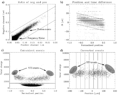
The STJ events can be discriminated from the absorber events by their spatial and spectral separation (fig. 5c). This is possible because the array is illuminated with monochromatic light. Part of the STJ events overlap with the outer absorber events in position and in case a broad band spectrum is used for illumination the spectral separation disappears. In order to calculate a correct measure for the photon energy and absorption position in the absorber the model of Jochum et al. (1993) is used (fig. 5d). Although this model is not complete in the description of all the processes involved with photon detection using DROIDs it provides an adequate and simple reconstruction method for the absorber events using only 2 fitting parameters (Hijmering et al. (2008)). The energy and position of absorption are derived from the measured signal amplitudes and as shown in equations (4) and (1).
| (1) |
Here is the conversion factor between the measured charge and photon energy which can be obtained by calibration. The values for the fitting parameters , corresponding to loss in the absorber, and , describing the trapping efficiency in the STJs, are determined from a least squares fit of the model to the absorber data, thus without the events in the STJs. The resulting values for and for the DROIDs in the array are averaged to obtain a single value for and which are then used for the correction. This is possible due to the homogeneity of the loss in the absorber and confinement of quasiparticles in the STJ in the DROIDs across the array. After this reconstruction is applied the absorber events are divided into 9 sections which are of roughly the same size as the STJs. The edges of the absorber in the data and the STJ events are determined by eye and the data points in between are separated in equidistant section. Each section will represent a virtual pixel in the final images.
5 Imaging quality of the DROID array detector
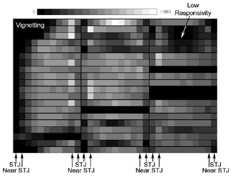
An image of a full illumination of the array (, the lower limit of the available wavelength band) is shown in fig. 6 illustrating the non-uniform response of the array. The left hand side of the image is affected by vignetting from the lens assembly. This is more prominent compared to all images shown below due to a shift sideways of the lens assembly due to a re-alignment. Four DROIDs were switched off and appear as 11 black pixels in a row, one in the second column, line 7, and 3 in the third column, lines 9, 10 and 13. The remaining non-uniformity is caused by the low responsivity of the devices in the following manner. The responsivity of some devices, such as in the upper right corner, is too low to lift the sum signal from an optical photon absorbed in the middle of the DROID above the threshold set to reject the coincident noise triggers (see fig. 5c) and these events are erroneously rejected as noise, producing dark areas in the image. If more energetic photons were used the signals of all events would rise above the thresholds and a much more uniform flat field would be obtained. The same holds for an array with higher responsivity. As long as the threshold settings as well as the wavelength of illumination remain unchanged, the above image can be used for flat field corrections on other images. At the positions where the flat field shows no events, e.g. due to vignetting, the correction factor is set to unity and no correction is applied.
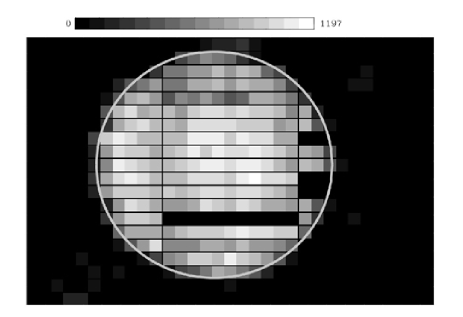
The imaging capabilities have been tested by illuminating the array through a set of masks positioned in the focus of the off-axis paraboidal mirror. Fig. 7 shows a reconstructed image for the case when the array was illuminated through a (diameter) aperture in the focus of the off axis paraboloidal mirror, which should be projected as a image on the detectors. The circle, which represents the predicted size of the image, overlaps the boundaries of the image indicating correct scaling and the sharp drop-off of the intensity at the edges suggests a correctly focussed image and good position resolution along the DROID.
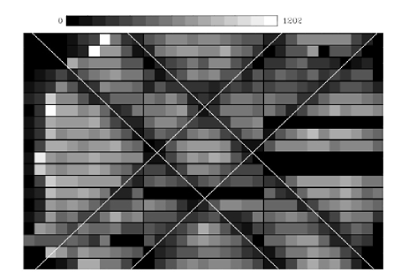
Secondly a mask with a double cross structure with line width of , corresponding to on the detector, was used. The spacing between the lines is in the focus which should result in a spacing of at the detector. Fig. 8 shows the resulting intensity plot with the projected image of the double cross represented by the lines. On the image the shadows of the double cross can be identified reasonably well and the lines overlap, showing the correct scaling. S-Cam is being developed for applications in ground based astronomy.
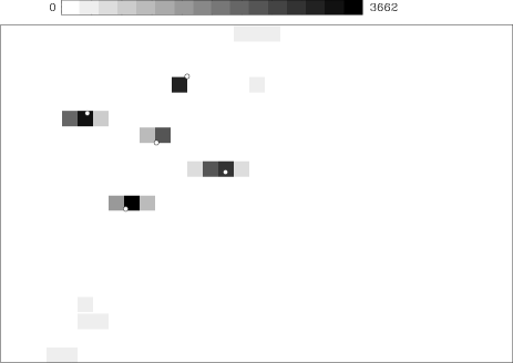
In order to simulate illumination from the sky a pinhole pattern has been located in the focus of the off axis parabola. Five pinholes are located on an grid which should result in five spots, close to the limit of the optics resolution, on a grid on the detector. Fig. 9 shows the resulting image in negative. The pinhole pattern is deliberately projected on an area of the array with good responsivity. The predicted size and positions of the spots on the array are plotted over the image. The spots do not perfectly overlap because the position resolution in the vertical direction is determined by the width of the absorber. The upper and middle points show less broadening along the DROID length. These spots are located directly on a STJ where, due to the lower energy gap and quasiparticle confinement, the energy and position resolution is improved. The broadening of the other three points is slightly above a virtual pixel and corresponds with the position resolving power of shown in section 2 as derived from the energy resolving power.
6 Discussion
We have successfully demonstrated the feasibility of a DROID array as an imaging detector in the UV/visible. The S-Cam 3 individual STJ array could easily be exchanged for the DROID array without introducing extra operating difficulties into the system. However, the larger superconducting area of the array appears to be more sensitive to trapping magnetic flux and better shielding inside the cryostat is required. The responsivity of the current array is too low for use on the telescope and only the shortest wavelengths in the available range of could be used. The responsivity is also non-uniform over the array, such that for some DROIDs not even the shortest wavelengths could be detected over the entire absorber. In order to reduce the effect on the images a flat field correction has been applied. The position resolution is found to be slightly larger than the absorber width as shown by illuminations with point sources as shown by fig. 9, and agrees with the position resolution of calculated from the energy resolving power. This position resolution is just adequate to replace 11 individual STJs with a single DROID. This corresponds to an array of 660 virtual pixels using only 120 readout channels which would amount to a field of view of on the William Herschel Telescope. The imaging capability of the DROID array has been demonstrated by using a aperture and a separated double cross with wide lines, fig. 7 and fig. 8. Both images show a recognisable image of the introduced object as expected from the good position resolution. The obvious first improvement on the DROID array for use on the telescope would be to increase the responsivity, which will automatically improve the energy and position resolution. This can be achieved by reducing the loss of quasiparticles inside the system. Experience has shown that the problem of low and variable responsivity appears to be related to the quality of the niobium interconnections between adjacent DROIDs and solutions are under investigation. In addition, increasing the thickness of the aluminium trapping layers in the STJ would improve the trapping of the quasiparticles in the STJs which will improve the responsivity thereby both energy and position resolution as well. Such performance has already been demonstrated in measurements on single DROIDs of identical geometry in Hijmering et al. (2006) and Hijmering et al. (2009). An aluminium layer thickness of 60nm is advised, which is a good trade off between the trapping in the STJs and thermal noise with the current base temperature of just below 300mK. There is also margin for decreasing the base temperature with more advanced sorption coolers which will allow even thicker Al layers to be considered. In addition to improvements on the DROID array some practical improvements can be introduced to the data acquisition system. Most important is to link the two readout chains for each DROID making it possible for the electronics to detect coincident events. If an event in one STJ is followed by an event in the other STJ within a user-determined time window the event is passed on as valid, otherwise it is discarded. Secondly, because the threshold on a single channel must be set low in order to detect the low signals in case of absorption near the opposite STJ a lot of coincident noise events will be passed. These can be effectively filtered out by introducing an extra threshold on the sum of the two pulse heights, effectively setting an upper wavelength limit for detection. These two modifications to the system would improve noise filtering and offline data reduction time by orders of magnitude. Finally the data could be converted into position and energy data instead of the charges of the STJs, by using for instance the model from Jochum et al. (1993). However care has to be taken where this is implemented. In order not to jeopardize the raw data it could be implemented in the pipeline software that converts the raw data file into the final data file for the user in FITS format (Pence (2009)), as for S-Cam 3. For the real-time analysis this can be performed in a parallel route to the operating software, e.g. using a lookup table to convert pulse height ratio into virtual pixel to save calculation time. This would provide a highly desirable real time preliminary image reconstruction.
7 Conclusion
We have successfully demonstrated operation of an array of DROIDs as a photon counting and imaging detector in an astronomical instrument. Although the responsivity of the array was too low for practical use, the resolving power and imaging capabilities, which will improve further with increasing responsivity, are already adequate. From this first system test we have obtained a good understanding on how to further optimize the system for photon detection with DROIDs.
References
- Bardeen et al. (1957) Bardeen J.,Cooper L., & Schrieffer J.R., 1957, Phys. Rev. 108, 1175
- Booth (1987) Booth N.E., 1987, Appl. Phys. Lett. 50, 293
- de Bruijne et al. (2002) de Bruijne J.H.J., Reynolds A.P., Perryman M.A.C., Favata F., Martin D., Verhoeve P., Rando N., & Peacock A., 2002, Galaxies: The Third Dimension, ASP Conf. Series 282, 565
- de Bruijne et al. (2002) de Bruijne J.H.J., Reynolds A.P., Perryman M.A.C., Peacock A., Favata F., Rando N., Martin D., Verhoeve P., & Christlieb N., 2002, A&A 381, 57
- Fano (1947) Fano U., 1947, Phys. Rev., 72, 26
- Pence (2009) Pence W.D., 2009, FITS, Flexible Image Transfer System, http://fits.gsfc.nasa.gov/
- Friedrich et al. (2006) Friedrich S., Lerch P., & Kirk E., 2006, Nucl. Instr. And Meth. A 559, 4779
- Hijmering et al. (2009) Hijmering R.A., Kozorezvo A.G., Verhoeve P., Martin D.D.E., Wigmore J.K., Venn R., & Groot P.J., 2009, submitted to J. Appl. Phys.
- Hijmering et al. (2008) Hijmering R.A., Verhoeve P., Kozorezov A.G., Martin D.D.E., Wigmore J.K., Jerjen I., Venn R., & Groot P.J., 2008, J. Appl. Phys. 103, 083914
- Hijmering et al. (2006) Hijmering R.A., Verhoeve P., Martin D.D.E., Peacock A., Kozorezov A.G., & Venn R., 2006 , Nucl. Instr. And Meth. A 559, 692
- Jochum et al. (1993) Jochum J., Kraus H., Gutsche M., Kemmather B., Feillitzsch F.v. , & Mössbauer R.L., 1993, Ann. Phys. (N.Y.) 2, 611
- Kraus et al. (1989) Kraus H., Feilitzsch F.v., Jochum J., Mössbauer R.L., Peterreins Th., & Pröbst F., 1989, Physics Lett. B 231, 195
- Kurakado et al. (1981) Kurakado M., & Mazaki H., 1981, Nucl. Instr. And Meth. 185, p. 141
- Martin (2007) Martin D.D.E., 2007, PhD thesis, University Twente
- Martin et al. (2003) Martin D.D.E., Verhoeve P., den Hartog R.H., de Bruijne J.H., Reynolds A.P., van Dordrecht A., Verveer J., & Peacock A.J., 2003, Proc. of SPIE 4841, 805
- Martin et al. (2006) Martin D.D.E., Verhoeve P., Oosterbroek T., Hijmering R.A., Peacock T., & Schulz R., 2006, Proc. of SPIE 6269, pp. 62690O
- Martin et al. (2004) Martin D.D.E., Verhoeve P., Peacock A., Dordrecht A. van, Verveer J., & Hijmering R.A., 2004, Nucl. Instr. And Meth. A 520, 512
- Mears et al. (1993) Mears C., Labov S.E., & Barfknecht A., 1993, Appl. Phys. Lett., 63, 2961
- Oosterbroek et al. (2006) Oosterbroek T., de Bruijne J.H.J., Martin D., Verhoeve P., Perryman M.A.C., Erd C., & Schulz R., 2006, A&A 456, 283
- Peacock et al. (1996) Peacock T., Verhoeve P., Rando N., Perryman M.A.C., Taylor B.G., & Jakobsen P., 1996, A&A 127, 581
- Perryman et al. (2001) Perryman M.A.C., Cropper M., Ramsay G., Favata F., Peacock A., Rando N., & Reynolds A., 2001, Monthly Notice of the Royal Astronomical Society 324, 899
- Perryman et al. (1999) Perryman M.A.C., Favata F., Peacock A., Rando N., & Taylor B.G., 1999, A&A 346, 30
- Prober et al. (2006) Prober D.E., Teufel J.D., Frunzio L., Wilson C.M., & Schoelkopf R.J., 2006, Nucl. Instr. And Meth. A 559, 676
- Rando et al. (2000) Rando N., Anderson S., Collaudin B., et al., 2000, Nucl. Instr. And Meth. A 444, 441
- Rando et al. (1991) Rando N., Peacock A., van Dordrecht A., Foden C.L., Engelhardt R., Taylor B.G., Gare P., Lumley J., & Pereira C., 1991, Nucl. Instr. and Meth., 313, 173
- Reynolds et al. (2003) Reynolds A.P., de Bruijne J.H.J., Perryman M.A.C., Peacock A., & Bridge C.M., 2003, A&A 400, 1209
- Romani et al. (1999) Romani R.W., Miller A.J., Cabrera B., & Figueroa-Feliciano E., 1999, Astrophys. J. 521, L153
- Verhoeve et al. (2002) Verhoeve P., Rando N., Peacock A., Martin D., & den Hartog R., 2002, Opt. Eng. 41 (6), 1170