Resonant Tunneling through S- and U-shaped Graphene Nanoribbons
Abstract
We theoretically investigate resonant tunneling through S- and U-shaped nanostructured graphene nanoribbons. A rich structure of resonant tunneling peaks are found eminating from different quasi-bound states in the middle region. The tunneling current can be turned on and off by varying the Fermi energy. Tunability of resonant tunneling is realized by changing the width of the left and/or right leads and without the use of any external gates.
pacs:
73.23.-b, 73.40.Gk, 73.40.Sx, 85.30.DeI INTRODUCTION
Graphene is a single layer of carbon atoms arranged in a hexagonal lattice that is the building block for graphite material. Recently, graphene samples have been fabricated experimentally by micro-mechanical cleavage of graphite Novoselov . This material has aroused increasing attention due to its novel transport properties that arises from its unique band structure: the conduction and valence bands meet conically at the two nonequivalent Dirac points, called and valleys of the Brillouin zone, which show opposite chirality. Around the two Dirac points, the energy dispersion is linear in momentum space and is well described by the massless Dirac-Weyl equation. The unique energy dispersion leads to a number of unusual electronic transport properties in graphene such as integer quantum Hall effect at room temperature QHE , finite minimal conductivity, and special Andreev reflection Beenakker1 ; Sengupta . In graphene electrons can pass through potential barriers without any reflection, i.e., the Klein tunneling, in contrast to conventional electrons that exhibit an exponential decreasing transmission with increasing barrier height and/or width. Klein tunneling makes it impossible to confine the carriers in single layer graphene using the electric gates that are often used in the conventional semiconductor two-dimensional electron gas (2DEG). Tunneling through single barriers Katsnelson and double barriers Pereira in graphene has been investigated theoretically. Recent theoretical work demonstrated that the magnetic barriers can be used to confine the massless Dirac fermion Egger and block the Klein tunneling and display a huge magnetoresistance Zhai ; Peeters . Klein tunneling leads to a poor rectification effect and the absence of resonant tunneling for normal incidence in graphene and limits the performance of graphene-based electronic devices.
In graphene nanoribbons (GNRs), the presence of edges can change the energy spectrum of the -electrons dramatically. GNRs can be fabricated using conventional lithography and etching techniques IBM ; kim . The electronic properties of a GNR depend very sensitively on the sizes and shape of the edges, i.e., zigzag- and armchair-edged GNR. The zigzag-edged graphene nanoribbons (ZGNRs) and armchair-edged graphene nanoribbons (AGNRs) exhibit very different band structures. The ZGNRs always have localized states appearing at the edge near the Dirac point, and therefore exhibit metallic-like behavior. The AGNRs show alternating metallic-like and semiconductor-like features alternatively as the width of nanoribbons increases Nakada . Such features are very different from the conventional semiconductor quantum wire and provide a unique way to tailor the transport properties of GNRs Wakabayashi ; Wakabayashi2 ; Peres ; Cresti ; Areshkin ; Yan . Recently it is found that single electronic potential barrier can block the electron tunneling in the ZGNRs and confine electrons in between double barriers Wakabayashi2 . The magnetic transport and spatial distribution of currents was investigated for unipolar and bipolar ZGNRs Cresti . These previous works have demonstrate that the resonant tunneling can be realized using electric and/or magnetic barrier. Here, we will address the question whether it is possible to realize resonant tunneling using only the geometry of the graphene nanoribbons. We focus on the S- and U-shaped structures consisting of zigzag leads and armchair nanoribbons in between them, because the zigzag nanoribbon is always metallic, while the bandgap of an armchair nanoribbon depends sensitively on the width of nanoribbon. This combination of zigzag and armchair nanoribbon could lead to interesting transport property.
In this work, we theoretically investigate the transport property through U-shaped nanoribbon structures sandwiched by two semi-infinite ZGNRs, i.e., the geometry of the graphene nanoribbon in the absence of any external nanostructured electric gates.. We will demonstrate resonant tunneling behavior through these graphene nanostructures whenever the AGNR in the middle part is metal-like or semiconductor-like. In those structures, the middle structure acts as a barrier between ZGNR leads, and an interesting resonant tunneling behavior can be seen with varying lengths of the middle part of the U-shaped ZGNR or AGNR.
This paper is organized as follows. In Sec. II, the theoretical model and calculation method are given. In Sec. III, we present the numerical results and our discussions. Finally we give our conclusion in Sec. IV.
II MODEL AND CALCULATION METHOD
To describe the electron transport through the S- or U-like structure sandwiched by two semi-infinite ZGNR leads, the tight-binding Hamiltonian is adopted
| (1) |
where creates (annihilates) an electron on site , is the nearest neighbor () hopping energy ( eV), and is the next-nearest neighbour () hopping energy Reich . The conductance of the system is evaluated using the Landauer-Büttiker formulabutiker ,
| (2) |
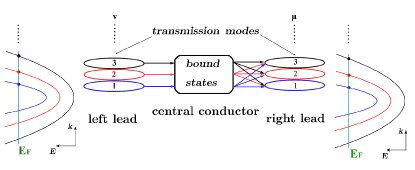
where is the transmission coefficient from the -th channel in the left lead to the -th channel in the right lead at the Fermi energy (as shown in Fig. 1), calculated by a recursive Green’s function method Ando , which is given as
| (3) |
where is the Fermi energy, is the effective Hamiltonian that equals the sum of the Hamiltonian of the central rectangular ring, , and the self energies of the semi-infinite leads in the left and right leads, . The key point of the recursion Green’s function method is that the middle conductor region is divided into many meshes, and consequently reduce the dimensionality of the Green’s function greatly. Therefore the computation of the conductance becomes more pratical.
The Fermi energy can be tuned experimentally through electric top- and/or back-gates Ozyilmaz . In our calculations, all physical quantities are dimensionless, e.g., the energy and the conductances are in units of and , respectively. The next-nearest neighbour hopping term is ignored because it is much weaker than that of the nearest neighbor hopping term, i.e., .
For completeness, here we repeat the essential steps in T. Ando’s work Ando to obtain recursive Green’s function . The equation of motion for an ideal lead can be written as:
| (4) |
where is the hamiltonian of a mesh in the ideal lead containing M lattice sites, is a vector describing the amplitudes of the mesh, and are the matrix blocks adjacent to in the total tight-binding Hamiltonian matrix. To obtain linearly solutions for Eq. 4, we first set . Substituting this in to Eq. 4 we have:
| (5) |
leads to the following eigenvalue problem:
| (6) |
We get the eigenvalues and corresponding eigenvectors, including M right-going and M left-going waves. We define the matrix for the eigenvalues and eigenvectors:
| (7) |
| (8) |
Now, we get the relations between and mesh:
| (9) |
with .
Next we consider the scattering in the middle conductor (from mesh 1to mash N) to both sides of witch an ideal wire is attached. By using Eq. 4 and Eq. 9, we obtain the effective hamiltonians (note that they are not hermitian) of the last mesh in left lead and first mesh in right lead, both adjacent to the middle conductor:
| (10) | |||
| (11) |
We can get the total effective hamiltonian matrix:
| (12) |
where for in the central region. Proceed by using Eq . 3 directly, we can obtain the desired recursive Green’s function .
III RESULTS AND DISCUSSIONS
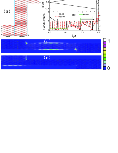
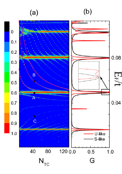
First, we discuss the transport property through the double-bended (S-shaped) GNR structure as shown in Fig. 2 (a) for reference purposes. Fig. 2 (c) shows the conductance as a function of the Fermi energy for different lengths of the AGNRs. There are the strong peaks in the conductance spectrum corresponding to the resonant tunneling process through the double-bended GNR structure. The underlying physics of such resonant tunneling process is that there are quasi-bound states in the middle conductor region which consists of the armchair and zigzag nanoribbons, the resonant tunneling occurs when the Fermi energy is equal to the energies of the quasi-bound states. The quasi-bound states arise from the propagation of electrons back and forth in the armchair region between the zigzag leads. The conductance of the perfect ZGNR displays a step-like feature, which corresponds to the opening of the different channels as the Fermi energy increases (see the green line in Fig. 2(c)). Note that we did not introduce any external electric field and/or gate to generate the barrier in the middle part. Therefore, this feature arises from the geometry effect, i.e., the different edges of the ZGNR leads and the AGNR conductor. As the Fermi energy increases, more incident channels are opened, the effect of the edge state becomes weaker, and the ratio between peaks and valleys of the conductance decreases (see the black and red lines in Fig. 2(c)). When the Fermi energy increases further and even becomes higher than the bottom of the second subband of the middle AGNR conductor (see the black vertical line in Fig. 2 (b)), the oscillation of the conductance becomes more significant. Fig. 2 (c) indicates that there are more tunneling peaks as the AGNR length increases. The incident electron can be completely reflected when the incident energy is less than the bottom of the second subband of the left ZGNR lead corresponding to the case of single mode incidence.
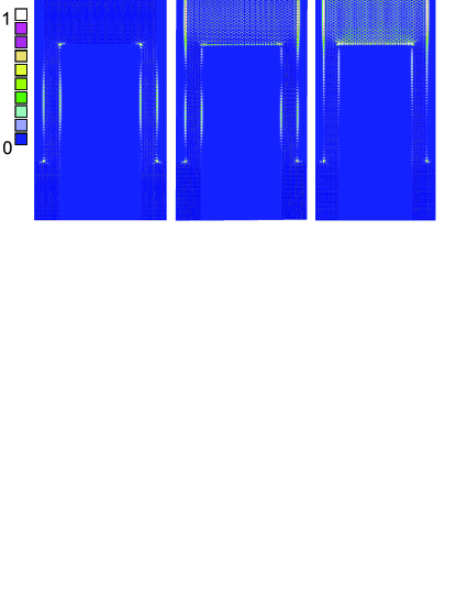
To obtain a clear physical picture, we plot the distribution of electron states at specific Fermi energies corresponding to the points A and B marked in Fig. 2 (c). Figure 2 shows the density distribution of the quasi-bound state in the middle AGNR part that contributes to the resonant tunneling (see the point A in Fig. 2 (c)). The electrons mainly localize at the edges of the middle AGNR, at the corner between the AGNR and ZGNR leads, and on the edge of AGNR. This quasi-bound state is quite different from the electron states of a perfect AGNR where no edge state appears due to the two different kinds of carbon atoms at the edges. But for the quasi-bound state, the electron state strongly localizes at the edges and especially at one kind of carbon atoms (see Figs. 2 (d) and (e)). This special quasi-bound state in the middle part contributes dominantly to the resonant tunneling process. We also plot the density distribution of the quasi-bound state corresponding to the completely reflection case (see point B in Fig. 2(c)) in Fig. 2(e). For this case, the electron state localizes at the edge of the left semi-infinite ZGNR lead near the interface between the lead and the middle conductor. In this case, the AGNR conductor can be used as an electron reflector. For the usual graphene nanoribbon, there is no quasi-bound state in the middle region since no armchair nanoribbon locates in between the zigzag leads. Therefore we can only observe the step-like feature of the conductance which corresponds to the opening of the channels with higher energies. (see the green line in Fig. 3(b))
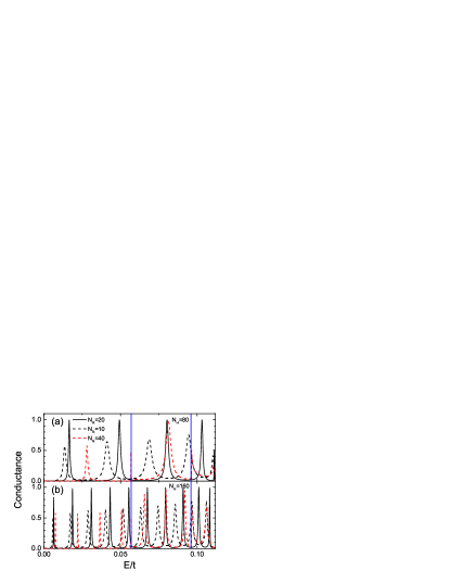
Next, we show how the width of the right lead affects the resonant tunneling behavior in Fig. 3. We fix the width of the left lead at while tuning the width of the right lead. In Fig. 3, the black solid, the black dashed, and the red dashed lines correspond to , and , respectively. Figure 3 (a) demonstates that the magnitude of the tunneling peaks decreases whether the width of the right lead is wider or narrower than that of the left lead. Thus the electrons cannot be fully transmitted through the nanostructure. The perfect transmission only takes place when the right lead has the same width as the left lead. When the width of the right lead is narrower than that of the left lead (see the black-dashed line in Fig. 3), the first tunneling peak is weakened heavily. When the Fermi energy increases, the magnitude and width of the tunneling peaks increase gradually. These increases are caused by the enhanced coupling between the quasi-bound states in the middle part and the leads. Comparing the case with equal widths of the left and right leads shown in Fig. 3 (a), all tunneling peaks for the wider (narrower) right leads shift to higher (lower) energy, and become sparse as the Fermi energy increases. For the wider right lead case, the conductance shows different features. For the Fermi energy below the bottom of the second subband in the right lead (see the first vertical green line), the variation of the magnitude of the tunneling peaks is similar to the case with the narrower right lead. When the Fermi energy is above the bottom of the second subband in the right lead, the magnitude of the tunneling peaks increases abruptly, even approaching to 1, and becomes wider (see the red dashed peaks in Fig. 5(b)). Comparing the conductances through the middle AGNR with different lengths () in Fig. 3, we find that the tunneling peaks become dense as the length increases. For longer AGNR (), the variation of the width of the right lead induces changes in the conductance similar to that of the shorter AGNR ().
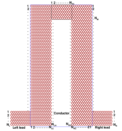
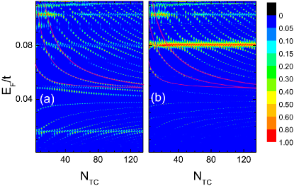
Now we turn to consider the U-shaped structure composed of two double-bend structures as shown in Fig. 4. Figure 5 (a) shows the contour plot of the conductance as a function of the length of the middle ZGNR bridge () and the Fermi energy () for the U-shaped structure. From this figure, the tunneling peaks show a periodic behavior as a function of the length . This period is exactly the same as that between the metal- and semiconductor-like AGNRs. The resonant tunneling processes can be divided into two kinds of processes according to the behavior of tunneling peaks varying with the length . The first kind of tunneling peaks is strong and does not shift when the length of the middle bridge increases, while the second kind shows the opposite behavior, i.e., shifting to lower and/or higher energies. Comparing the conductance of the U-shaped structure with that of one double-bended (S-shaped) structure, the four peaks in Fig. 5(b) correspond exactly to the tunneling peaks of the double-bended structure (S-shaped) (see Figs. 5 (a) and (b)). Therefore these resonant tunneling processes are caused by the quasi-bound states localized in the two AGNR regions in the middle conductor parts, which behave like the resonant tunneling through a single barrier. This can be understood from the spatial distribution of the quasi-bound states contributing to the resonant tunneling process marked by point A in Fig. 5(a). The quasi-bound electron state localizes at the left and right AGNR of the middle conductor. From the inset of Fig. 5(b), one can see that the first kind resonant peak near E=0.05t split into two peaks due to the coupling between the two lowest localized states in the left and right AGNRs through the ZGNR bridge, i.e, the bonding and antibonding splitting. Therefore the resonant peaks split into two peaks and show an anticrossing behavior with increasing the length of ZGNR bridge that describes the coupling strength. The other resonant tunneling peaks are shaper and are located between the strong tunneling peaks mentioned above and vary as the length increases (see Fig. 5 (a)). Those peaks is the result of the resonant tunneling processes through the double barriers, since the corresponding quasi-bound states localize in the ZGNR bridge of the middle conductor. These quasi-bound states mainly distribute in the ZGNR bridge, especially at the two vertical edges of the ZGNR bridge (see Fig. 6 (b) and (c)). The spatial distributions of the quasi-bound states show the antibonding (Fig. 6 (b)) and bonding (Fig. 6 (c)) states corresponding to the resonant tunneling peaks B and C marked in Fig. 6(a). This bonding and antibonding feature also explain why the positions of the resonant tunneling peaks B (C) decrease (increase) as the length increases.
Finally, we investigate the effect of the widths of the right lead on the transport property. We fix the width of the left lead at while tuning the width of the right lead. Figure 7 (a) shows the contour plot of the conductance as a function of the Fermi energy and the length of the ZGNR bridge for the width of the right lead . The figure shows that the first kind of tunneling peaks disappears but the second kind of tunneling peaks still can be observed, because the latter is a consequence of tunneling through the quasi-bound states localized in the middle bridge. The effect of the width of the lead on the second kind of tunneling processes is much weaker than on the first kind of tunneling processes. For the wider right lead in Fig. 7 (b), the situation is similar with . But when the Fermi energy is larger than the bottom of the second subband of the right lead, a strong tunneling process appears at . With a wider or narrower right lead, the second kind of tunneling processes display similar behavior as the length () of the bridge increases. The tunneling processes induced by the quasi-bound antibonding states results in tunneling peaks with an energy that is approximately 0.04t higher. Those peaks shift to lower energy as the length of the bridge increases. In contrast, opposite behavior as compared to those induced by the antibonding states, i.e. the blue shift.
IV CONCLUSIONS
In summary, we investigated theoretically the transport properties of carriers that move through S-and U-shaped graphene nanoribbons. We found that as function of the Fermi energy the tunneling current can be turned on and off periodically making this device suitable for transistor action. We demonstrated that resonant tunneling can be realized utilizing the geometrical effect of such bended GNR structures even in the absence of any nanostructured gates. The strong resonant tunneling processes arise from the quasi-bound states that localize at the middle part and can be clearly seen in the conductance spectra. The spectra exhibits rich structures coming from the different kind of quasi-bound states in the middle part. The resonant tunneling processes can be tuned by changing the Fermi energy and the width of the left and right leads. Our theoretical results demonstrate that resonant tunneling can be realized utilizing the geometry of the graphene nanoribbon without any nanostructured electric gates. We believe that our theoretical results are interesting both for the basic physics and for the potential application of electronic devices based on graphene nanoribbons.
Acknowledgements.
This work is supported by the NSF of China Grant No. 60525405 and 10874175, the Flemish Science Foundation (FWO-Vl) and the Belgian Science policy.References
- (1) K. S. Novoselov, A. K. Geim, S. V. Morozov, D. Jiang, Y. Zhang, S. V. Dubonos, I. V. Grigorieva, and A. A. Firsov, Science 306, 666 (2004).
- (2) Y. Zhang, Y. Tan, Horst L. Stormer, and P. Kim, Nature 438, 201 (2005); K. S. Novoselov, Z. Jiang, Y. Zhang, S. V. Morozov, H. L. Stormer, U. Zeitler, J. C. Maan, G. S. Boebinger, P. Kim, and A. K. Geim, Science 315, 1379 (2007).
- (3) C. W. J. Beenakker, Phys. Rev. Lett. 97 067007 (2006).
- (4) S. Bhattacharjee and K. Sengupta, Phys. Rev. Lett. 97 217001 (2006).
- (5) M. I. Katsnelson, K. S. Novoselov, and A. K. Geim, Nat. Phys. 2, 620 (2006).
- (6) J. M. Pereira, P. Vasilopoulos, and F. M. Peeters, Appl. Phys. Lett. 90 132122 (2007).
- (7) A. De Martino, L. Dell’Anna, and R. Egger, Phys. Rev. Lett. 98, 066802 (2007).
- (8) F. Zhai and Kai Chang, Phys. Rev. B 77, 113409 (2008).
- (9) M. Ramezani Masir, P. Vasilopoulos, A. Matulis, and F.M. Peeters, Phys. Rev. B 77, 235443 (2008)
- (10) Z. H. Chen, Y. M. Lin, M. J. Rooks, and P. Avouris, Physica E 40, 228 (2007).
- (11) M. Y. Han, B. Ozyilmaz, Y. B. Zhang, and P. Kim, Phys. Rev. Lett. 98, 206805 (2007).
- (12) K. Nakada, M. Fujita, G. Dresselhaus, and M. S. Dresselhaus, Phys. Rev. B 54, 17954 (1996).
- (13) K. Wakabayashi, Phys. Rev. B 64, 125428 (2001).
- (14) K. Wakabayashi and T. Aoki, Inte. J. Mod. Phys. B 16, 4897 (2002).
- (15) N. M. R. Peres, A. H. Castro Neto, and F. Guinea, Phys. Rev. B 73, 195411 (2006).
- (16) A. Cresti, G. Grosso, and G. P. Parravicini, Phys. Rev. B 77, 233402 (2008).
- (17) D. A. Areshkin, D. Gunlycke, and C. T. White, Nano Lett. 7, 204 (2007).
- (18) Q. M. Yan, B. Huang, J. Yu, F. W. Zheng, J. Zang, J. Wu, B. L. Gu, F. Liu, and W. H. Duan, Nano Lett. 7, 1469 (2007).
- (19) S. Reich, J. Maultzsch, C. Thomsen, and P. Ordejn, Phys. Rev. B 66, 035412 (2002).
- (20) M. Büttiker, Y. Imry, R. Landauer, and S. Pinhas, Phys. Rev. B 31, 6207 (1985).
- (21) T. Ando, Phys. Rev. B 44, 8017 (1991).
- (22) B. Ozyilmaz, P. Jarillo-Herrero, D. Efetov, D. A. Abanin, L. S. Levitov, and P. Kim, Phys. Rev. Lett. 99 166804 (2007).