Magnetic interference patterns in SIFS Josephson junctions: effects of asymmetry between and regions
Abstract
We present a detailed analysis of the dependence of the critical current on the magnetic field of , , and superconductor-insulator-ferromagnet-superconductor Josephson junctions. of the and junction closely follows a Fraunhofer pattern, indicating a homogeneous critical current density . The maximum of is slightly shifted along the field axis, pointing to a small remanent in-plane magnetization of the F-layer along the field axis. of the junction exhibits the characteristic central minimum. however has a finite value here, due to an asymmetry of in the and part. In addition, this exhibits asymmetric maxima and bumped minima. To explain these features in detail, flux penetration being different in the part and the part needs to be taken into account. We discuss this asymmetry in relation to the magnetic properties of the F-layer and the fabrication technique used to produce the junctions.
pacs:
74.50.+r,85.25.Cp 74.78.Fk 74.81.-gI Introduction
While predicted more than 30 years agoBulaevskiĭ et al. (1977); Buzdin et al. (1982), due to the severe technological requirements, the experimental study of Josephson junctions became an intense field of research only recently. Superconductor-ferromagnet-superconductor (SFS) Josephson junctions were successfully fabricated and studiedRyazanov et al. (2001); Sellier et al. (2004); Blum et al. (2002); Bauer et al. (2004). SFS junctions however typically exhibit only very small (metallic) resistances , making this type of junctions less suitable for the study of dynamic junction properties as well as for applications, where active Josephson junctions are required. To overcome this problem, an additional insulating (I) layer can be used to increase , although at the expense of a highly reduced critical current density Kontos et al. (2002); Weides et al. (2006a); Bannykh et al. (2009); Sprungmann et al. (2009).
In a SFS or SIFS junction the proximity effect in the ferromagnetic layer leads to a damped oscillation of the superconducting order parameter in the F-layer. Thus, depending on the thickness of the F-layer, the sign of the order parameters in the superconducting electrodes may be equal or not. While in the first case a conventional Josephson junction (a “ junction”) with is realized, in the latter case a “ junction” is formed where the Josephson current obeys the relation . Here is the junction critical current and is the phase difference of the order parameters in the two electrodes.
The combination of a and a part within a single Josephson junction leads to a “” Josephson junction. Depending on several parameters of the and part, a spontaneous fractional vortex may appear at the boundaryBulaevskiĭ et al. (1978). In case of long junctions with length the vortex contains a flux equal to a half of a flux quantum . Here is the Josephson length; is the magnetic permeability of the vacuum and is the London penetration depth of both electrodes.
Up to now three different types of Josephson junctions exist. One approach makes use of the wave order parameter symmetry in cuprate superconductorsHarlingen (1995); Tsuei and Kirtley (2000); Chesca et al. (2002); Smilde et al. (2002); Ariando et al. (2005). Another approach is to use standard Josephson junctions equipped with current injectorsUstinov (2002); Goldobin et al. (2004) which allow to create any phase shift. Josephson junctions were also produced (accidentally) by SFS technologyDellaRocca et al. (2005); Frolov et al. (2006). The first intentionally made SIFS junction including reference and Josephson junctions fabricated in the same run were recently realizedWeides et al. (2006b). Some static and dynamic properties of this type of junction were studied experimentallyWeides et al. (2006b, 2007a); Pfeiffer et al. (2008). Relevant theoretical work on SIFS junctions can be found in Vasenko et al. (2008); Volkov and Efetov (2009).
The aim of the present paper is to provide a careful analysis of the magnetic field dependence of the junction critical current in order to characterize these novel type of junctions as accurately as possible. The (short) junction we discuss has a length . As we will see, the measured can be reproduced very well when, apart from asymmetries of the critical current densities in the and parts, asymmetric flux penetration into the and parts is taken into account.
The paper is organized as follows: In section II the SIFS junctions are characterized in terms of geometry, and the properties of the F-layer are further characterized by measuring the magnetization of a bare thin films with thickness comparable to the F-layer used for the junctions. In the central section III the magnetic field dependence of the critical current of the SIFS junctions is discussed. Section IV contains the conclusion.
II Sample characterization
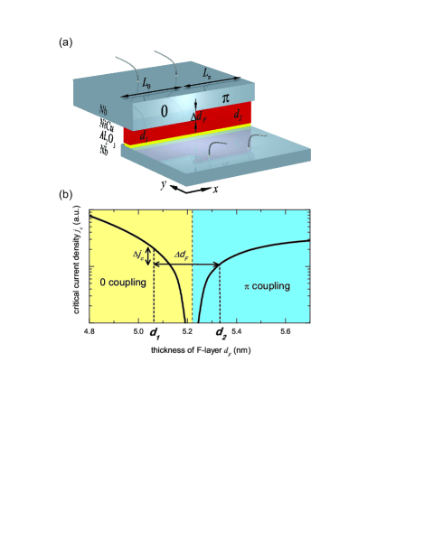
Fig. 1(a) shows a sketch of the junction used in the experiment. The superconducting bottom and top layers consist of Nb with the thicknesses and , respectively. As for standard Nb tunnel junctions an layer was used as tunnel barrier. Its thickness is , determined from dynamic measurements. For the ferromagnetic layer we use the diluted ferromagnet . To form a junction the junction is divided into two parts differing by the thickness of the F-layer. While in one half of the junction the thickness is chosen such that coupling is realized, in the other half the F layer thickness is used to realize coupling. In order to have approximately symmetric junctions, and should be such that the critical current densities of the two halves are about the same and as large as possible, see Fig. 1(b).
Details of the fabrication technique can be found in Refs. Weides et al., 2007b, a. The main feature is a gradient in the ferromagnetic layer along the direction of the 4” wafer, in order to allow for a variety of and coupled junctions differing in their critical current densities. In addition, by optical lithography and controlled etching, parts of the F-layer are thinned by , such that coupling is achieved in these parts. Thus the chip contains un-etched parts with F-layer thickness , as well as uniformly etched parts with F-layer thickness . Thus, at a fixed -position we have two different ferromagnetic thicknesses allowing for patterning a set of three junctions:
-
a junction with F-layer thickness and critical current density
-
a junction with F-layer thickness and critical current density
-
a stepped junction with thicknesses , and critical densities , in and halves.
For the values and we achieved and at , as estimated from and reference junctions. Due to the different temperature dependence of and (see Ref. Weides et al., 2006a) these values change to at .
All junctions had the same geometrical dimensions , see Fig. 2. The superconducting electrodes extend well beyond the junction area, leading to an idle region around the junction affecting the Josephson length . Ignoring this correction, using , as measured at , one finds , i.e. as in Ref. Weides et al., 2006b. The idle region of width in direction leads to an effective Josephson lengthMonaco et al. (1995)
with the junction width , and the inductances (per square) of the superconducting films forming the junction electrodes
and the idle regions . For our junction we get
, with ,
, , and
. Therefore the normalized junction length at
is and
we clearly are in the short
junction limit.
Magnetic properties of the F-layer
In order to investigate the magnetic properties of the
alloy used for the F-layer we performed
measurements of the magnetization via SQUID magnetometry.
The sample was a thin
film deposited directly on a substrate.
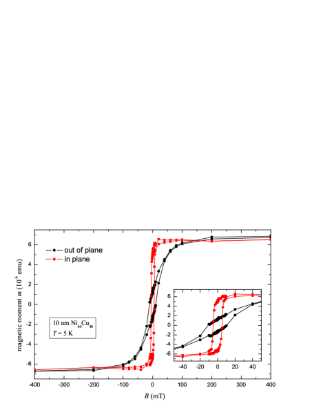
The obtained magnetization curves (after diamagnetic correction) at are shown in Fig. 3 for the magnetic field applied in-plane or out-of plane. The magnetic moments for the out-of plane and in-plane component saturate at almost equal corresponding to a saturation magnetization . Using the density (bulk value) of the F-layer and the molar weight we can estimate the atomic saturation moment , in good agreement with found in literature Ahern et al. (1958).
In the inset of Fig. 3 the hysteresis of the magnetization curves is shown at small applied magnetic fields. Remanence can be seen for the in-plane as well as the out-of plane curves. The inversion of the magnetizations is smooth, indicating a multiple domain state. The magnetic field necessary to fully magnetize the magnetic film in-plane is in the order of , whereas the out-of plane magnetization saturates above about . Therefore we expect the in-plane magnetization to be energetically favorable.
Both saturation fields are orders of magnitude larger than the in-plane fields typically used for SIFS critical current versus magnetic field measurements. In the following we estimate an upper limit by
how much the pattern (of a junction or a
junction) would shift along the field axis for an in-plane, fully
saturated ferromagnetic layer. Our measured saturation magnetization yields a magnetic induction . A cross section of length and a thickness encloses an intrinsic
magnetic flux .
For and
the magnetic flux is
. Thus, the pattern would be shifted along the field axis
by about periods, while in experiment typically shifts of much
less than one period are observed. Further, nearly all our SIFS
junctions had mirror-symmetrical patterns for
, again strongly indicating that the F-layer
is in a multiple domain state with a very small in-plane net
magnetic flux Weides (2008). The out-of-plane net magnetic flux has
to be small too. As we will see in the next section, for the
and junctions highly symmetric patterns can be
measured. If the out-of-plane magnetic flux were very large, one
would expect a large number of Abrikosov vortices penetrating the
superconducting layers, making the of SIFS junctions with a
planar F-layer strongly asymmetric.
The ferromagnetic properties of a comparable ferromagnetic
compound, , were investigated recently via anomalous Hall voltage
measurements and Bitter decoration techniques of the magnetic domain
structures Veshchunov et al. (2008), indicating a magnetic anisotropy and a
magnetic structure with domains of about
in size. Both Hall and Bitter decoration measurements are only sensitive to out-of-plane components of the magnetic fields, and the growth conditions of the sample in Ref. Veshchunov et al., 2008 may influence its magnetic properties. Nevertheless it supports our experimental findings of a very small in-plane magnetization for zero field cooled samples and a multiple domain state in the F-layer of our SIFS devices.
III critical current vs. magnetic field
In order to measure the magnetic field dependence of the critical
currents of our junctions, the samples were mounted in a glass-fiber
Helium cryostat surrounded by a triple mu-metal shield. To minimize
external noise the whole setup was placed in a high-frequency screnning
room, the current leads were low-pass filtered, and all electronics
within the screnning room was powered by batteries. The sample was
initially cooled from room-temperature down to with the
sample mounted inside the magnetic shield. To remove magnetic flux
sometimes trapped in the superconducting electrodes the sample was
thermally cycled to above the superconducting transition temperature
. To determine we used a voltage criterion of
. The current-voltage () characteristics and
were measured for all three junctions at various
temperatures . The magnetic field was
applied along the direction see Fig. 1(a).
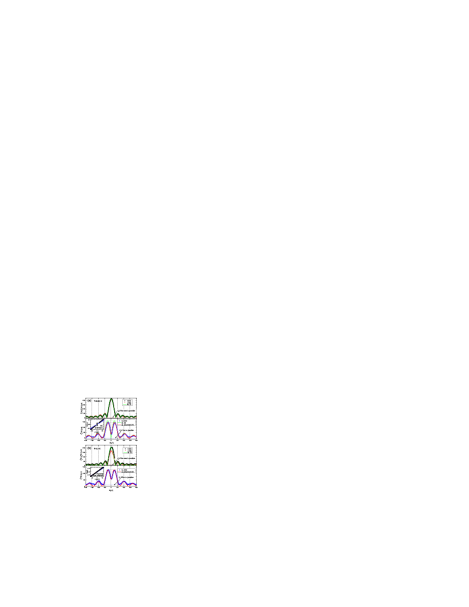
Figure 4 shows measurements of at (a) and (b) . Together with the experimental data we plot theoretical curves using the analytic expressions valid for short junctions having homogenous critical current density.
For the and junctions one has the Fraunhofer pattern:
| (1) |
where is the number of the applied
flux quanta through the normalized junction area , with .
For a symmetric, short junction the analytical expression
is given by Wollman et al. (1995); Xu et al. (1995):
| (2) |
At the reference junctions have basically the same maximum critical current of and and are fitted very well by the standard Fraunhofer curve given by Eq. (1). Note that the maximum is shifted along the axis by a few percent of one flux quantum. For reference we also show by a dotted horizontal line the -detection limit set by the finite voltage criterion. Here denotes the (subgap) junction resistance at small voltage. was estimated from the corresponding -curves shown in the insets of Fig. 4. For the measurements at this line is marginally shifted from zero.
Looking at of the stepped junction at (see bottom graph of Fig. 4(a)), we see that the agreement between the analytical expression Eq. (2) and the measurement is worse than for the reference junctions. For example the central minimum of is reproduced qualitatively, however, apart from a slight shift to positive magnetic field values, it does not reach zero critical current and is U-shaped in contrast to the V-shaped central minimum predicted by Eq. (2). Further, the side maxima in at the magnetic field are below the theoretical value of . Additionally we found a small asymmetry of the maxima of , i.e. and . Finally, the first side minima of were reached at the same magnetic field () as the second minima of the of the reference junctions, but exhibit bumps and do not reach zero-level defined by the line.
All discrepancies to the calculated pattern, especially the non-vanishing minima, are not due
to our measurement technique. All characteristic features are well
above our detection limit, drawn by the dotted line in the
bottom graph of Fig. 4(a). The U-shaped central
minimum could be due to fluctuations in the applied
magnetic field. However, careful measurements using superconducting
magnetic field coils in persistent mode to exclude any magnetic field
noise showed no further decrease of the minimum. An improved fit can
be achieved by assuming that the critical current densities of the
two halves of the junction are not identical, i.e. are
different from the respective and of the reference
junctions (e.g. caused by some gradient of the ferromagnetic
thickness along direction; the distance between reference and
stepped junctions on the chip is about ). The
dashed line in the bottom graph of Fig. 4(a) shows
the result of a corresponding calculation (the procedure is
discussed further below) using . While the critical
current value of the central minimum is reproduced reasonably well,
the other discrepancies remain.
Fig. 4(b) shows data for . The
critical currents of the and reference junction differ by
, but still are reasonably well described by the
Fraunhofer pattern Eq. (2). The main
discrepancy between fit and measurements can be found in the minima
of . The experimental minima do not reach zero current,
which at this temperature is due to the finite voltage criterion,
c.f. horizontal dotted lines. The lower graph in Fig.
4(b) shows the corresponding measurement for
the junction together with a theoretical curve, using
. Although the overall agreement between the two curves
is reasonable, again the shape of the minima is not reproduced well.
To further discuss the observed discrepancies we either have to assume, that and are non-uniform over the junction length, which would be contradictory to the observations at the reference junctions, or we should consider effects caused by a possible remanent magnetization of the F-layer, which can be different in the and part, plus the possibility that the magnetic flux generated by the applied field may be enhanced by the magnetic moment of the F-layer. Also, the effective junction thickness may be different in the and parts, causing additional asymmetries. To account for these effects, the local phases in the two parts may be written as
| (3) | |||
| (4) |
Here, is an initial phase to be fixed when calculating the total critical current. are the fluxes, normalized to , that are generated by the (1D) -component of the in-plane remanent magnetizations in the and parts, respectively. are the normalized fluxes through the junction generated by the applied magnetic field. In the following we parameterize as and as , respectively. We further set which is the case for the sample discussed here.
To obtain the junction critical current as a function of the applied magnetic field, we first calculate the currents , in the and parts via
and maximize with respect to for each value of the applied magnetic field.
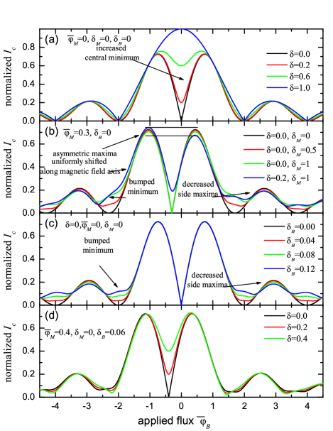
We first address the effect of the parameters , , , and on the patterns, c.f. Fig. 5(a) to (d).
If only a asymmetry is considered, as shown in Fig. 5(a), using definitions , , and , one finds that with increasing asymmetry the central minimum increases (for one reaches the extremum of a non-stepped junction with length , while the part becomes “non-Josephson” with ). However in all cases the first side maxima remain symmetric and the side minima reach zero current.
Next we would like to take into account the effect of the flux generated by remanent magnetizations. If we consider only a non-zero magnetization, i.e. , with all other parameters being zero, the curve gets shifted along the field axis, since the total flux in the junction is just the sum of applied field and magnetization. This can be seen in Fig. 5(b) (black curve). By adding an asymmetry the side minima get bumped and at the same time the maxima decrease (c.f. Fig. 5(b) red curve). However the curve is still symmetric with respect to the central minimum. This changes by adding an additional asymmetry in the critical current densities. Now the two main maxima get asymmetric and the side minima get bumped (blue curve).
Now we want to consider the effect of asymmetric flux in the and halves, i.e. we look at . In Fig. 5(c) we show the results obtained by increasing with the other parameters kept at zero. The increase of leads to bumped minima and decreased side maxima. The resulting curves looks similar to the ones shown in Fig. 5 (b) with asymmetries in the magnetization . The comparison reveals that the parameter acts much stronger than . The curve is still symmetric with respect to the central minimum.
In Fig. 5(d) we add a remanent magnetization without asymmetry, i.e. and , and allow asymmetric critical currents . As one can see the maxima remain symmetric whereas the minima get slightly asymmetric.
We further note that the calculated patterns are identical if we simultaneously change the sign of , , and . Thus the pattern of the junction only does not allow to identify which parameters belong to the and part. However the additional information on the (temperature dependent) critical current densities of the reference junctions may allow a clear identification of and .
Using the above findings on the parameters , , , and we next discuss our experimental data. For the non-vanishing central minimum in a critical current asymmetry is required and the shift along the magnetic field axis can solely be caused by a finite value of . Thus there are only two non-trivial parameters (, ) left to reproduce the remaining features of the experimental data.
If one allows for an asymmetry in the remanent magnetizations only, i.e. and , it is not possible to reproduce the experimental at low and high magnetic fields at the same time. The resulting curves can be seen in Fig. 6(a). For large (Fig. 6(a) dashed green line) the fit works well for high fields but fails in the first side minima. With a smaller value of (Fig. 6(a) solid red line) the situation is opposite.
By contrast the parameter (with ) leads to a good agreement between the theoretical and experimental pattern.This is shown in Fig. 6(b) where we used . There are only small asymmetries near the side maxima and minima that cannot be reproduced for the case . If we use both asymmetry parameters we get an excellent agreement of the theory with the experimental data, as shown in Fig. 6(c) for the data.
To further test the fit procedure we now use the data and assume that the magnetic parameters remain the same as for . By contrast will change due to a different temperature dependence of and , as already discussed above. For we get a reasonable agreement, as shown in Fig. 7.
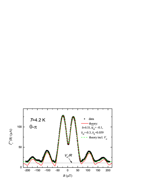
The fit is apparently not as good as the fit. However note that at 4.2 K the detection limit is much higher and the minima in are limited by the finite voltage criterion. Still some of the bumps appear at the same values of applied field both in the experimental and theoretical curve.
For the sake of completeness we also consider the effect of the finite voltage criterion. Using the expression describing the current-voltage characteristics of a Josephson junction in the framework of the resistively shunted junction (RSJ) modelStewart (1968); McCumber (1968) we get a corrected via , where refers to the theoretical curve (solid curve in Fig. 7). The corrected curve is shown as dashed (green) line in Fig. 7. As can be seen the data are reproduced perfectly.
Discussion of the obtained parameters
Finally, we would like to discuss the parameters which are obtained by fitting the experimental data. As already mentioned above, the parameters , , , and allow to find the different parameter sets for the two halves of the junction. For the distinction between “” and “” additional information is needed, which we get from the reference junctions.
The parameter allows to extract the absolute values of the critical current densities in the two parts. We get an almost temperature independent critical current density in the one half with . By contrast, for the other part we find a temperature dependent current density with to . A comparison with the temperature dependencies of the reference junctions allows the identification that the first part has to be coupled, whereas the second part is coupled. The absolute values of of the and junction are approximately the same whereas of the junction is reduced by as compared to the reference junction, although the temperature dependence looks very similar. This indicates a slightly reduced thickness of the F-layer in the part of the junction, c.f. Figure 1(b). Taking the data of Ref. Weides et al., 2006a the difference in thickness can be estimated to be . This may be caused by some gradient of the ferromagnetic thickness along direction on the chip, as the distance between reference and stepped junctions on the chip is about .
The parameters related to a different remanent magnetization in the and part, i.e. and , seem reasonable. The magnetization is of the order of of a fully saturated magnetization, indicating that the F-layer is in a multi-domain state. Note that the resulting magnetization of the part is larger than the magnetization of the part, which seems realistic due to a thicker F-layer in the part. In fact, the ratio of the F-layer thicknesses is very close to 1, so, assuming that magnetization is proportional to the volume of the F-layer in each part, it is quite difficult to explain the above value of . However, if one assumes that there is a dead layer of thickness one can calculate its value from
to be . This value is somewhat larger than estimated earlier from a fit made for a different run of the same fabrication processWeides et al. (2006a). However, as we see from Figs. 6 (b) and (c) the change in from to affects only the tiny features on the curve. Thus, the value of cannot be found from this fit very exactly.
Besides the current asymmetry the most important parameter for our experiment is the asymmetry parameter . Using a finite and almost all features could be reproduced very well. The addition of the parameters related to remanent magnetizations lead to minor improvements in the agreement of theory and experiment. In the following we want to discuss three possible scenarios causing the asymmetry .
First, the effect could be caused simply via the fabrication procedure of the junction. In the part of the junction the SF bilayer was deposited in situ whereas the Nb cap layer in the part was deposited after an etching process. Thus the properties, such as the mean free path and hence the London penetration depth , of the Nb cap layers in the two halves could easily differ by few percents.
Second, one could think of a paramagnetic component in the magnetization. As already discussed above, the F-layer is expected to be in a multi-domain state with a small net magnetization in-plane. An external field applied in-plane could cause a reconfiguration of the domains. In the two halves the pinning of the domains may be different, due to the different thicknesses and the different treatment. This would result in a asymmetric field dependent magnetization.
A third possibility is the appearance of an enhanced flux penetration due to inverse proximity effect, causing a correction in the London penetration depth. Due to the reduction of the order parameter in the vicinity of the ferromagnetic layer, the effective penetration depth might be enlarged. In order to estimate this effect, we calculated numerically the space-dependent superfluid density in the superconducting and the ferromagnetic part of the SF bilayer using the quasiclassical approachVasenko et al. (2008). Herein we used the parameters of our SF bilayer, which were already obtained in Ref. Vasenko et al., 2008 by fitting the experimental data of Ref. Weides et al., 2006a . By using the (London) expression we obtained the spatial dependence of the penetration depth. Then we used the second London equation to calculate the magnetic field numerically. We define the effective penetration depth as , with and being the flux in our SF bilayer with and without inverse proximity corrections. For our SIFS junctions with a thickness of the ferromagnet and of the top electrode we get at . Therefore in our case the inverse proximity corrections are negligible. In addition the corrections due to inverse proximity effect would be opposite in sign, i.e. , in contrast to found for our junction.
By looking at the other two scenarios it seems natural that the fabrication procedure causes the observed asymmetry. However at the moment, we cannot exclude a field-dependence of the magnetization. A clarification deserves further investigations.
IV Conclusions
In this paper we presented a detailed analysis of the magnetic field dependence in the critical current, , in , , and SIFS Josephson junctions. The length of the junctions is smaller than the Josephson length. The pattern of the and the junction can be well described by the standard Fraunhofer pattern, valid for a homogenous, short junction. The central maximum of this pattern is typically shifted from zero by some percent of one flux quantum, pointing to a weak in-plane magnetization of the F-layer. The magnetization is of order of of a fully saturated magnetization, indicating that the F-layer is in a multi-domain state.
The pattern of the junction exhibits the central minimum, well known for this type of junction. However the critical current at this minimum is non-zero, pointing to an asymmetry in the critical current densities in the two halves of the junction. In addition exhibits asymmetric maxima and bumped minima that cannot be described exclusively by critical current asymmetries. A detailed explanation of these features requires the consideration of asymmetric fluxes generated in the and parts of the junction. A careful analysis of the experimental data and our model showed that the majority of the observed discrepancies are due to a field-dependent asymmetry of the fluxes in the and part. The effect could either be caused by a small, field-dependent, in-plane magnetization of the F-layer or by a difference in the penetration lengths, which most naturally can be due to the fabrication technique. In principle, this effect should also be present in the ’s of the reference junctions. However, here the effect only leads to a small scaling factor for the magnetic field, which is too small to be detectable in experiment, e.g. if the effects of field focusing are considered.
The model discussed in this paper on the basis of junctions can be extended, e.g., to SIFS junctions having step-like profileWeides (2009), or laterally ordered ferromagnetic domains.
Acknowledgment
This work is supported by the Deutsche Forschungsgemeinschaft (DFG) via the SFB/TRR 21 and project GO 944/3. M. Kemmler acknowledges support by the Carl-Zeiss Stiftung. M. Weides is supported by DFG project WE 4359/1-1.
References
- Bulaevskiĭ et al. (1977) L. Bulaevskiĭ, V. Kuziĭ, and A. Sobyanin, JETP Lett. 25, 290 (1977).
- Buzdin et al. (1982) A. I. Buzdin, L. N. Bulaevskiĭ, and S. V. Panyukov, JETP Lett. 35, 178 (1982).
- Ryazanov et al. (2001) V. V. Ryazanov, V. A. Oboznov, A. Y. Rusanov, A. V. Veretennikov, A. A. Golubov, and J. Aarts, Phys. Rev. Lett. 86, 2427 (2001).
- Sellier et al. (2004) H. Sellier, C. Baraduc, F. Lefloch, and R. Calemczuk, Phys. Rev. Lett. 92, 257005 (2004).
- Blum et al. (2002) Y. Blum, A. Tsukernik, M. Karpovski, and A. Palevski, Phys. Rev. Lett. 89, 187004 (2002).
- Bauer et al. (2004) A. Bauer, J. Bentner, M. Aprili, M. L. D. Rocca, M. Reinwald, W. Wegscheider, and C. Strunk, Phys. Rev. Lett 92, 217001 (2004).
- Kontos et al. (2002) T. Kontos, M. Aprili, J. Lesueur, F. Genet, B. Stephanidis, and R. Boursier, Phys. Rev. Lett. 89, 137007 (2002).
- Weides et al. (2006a) M. Weides, M. Kemmler, E. Goldobin, D. Koelle, R. Kleiner, H. Kohlstedt, and A. Buzdin, Appl. Phys. Lett. 89, 122511 (2006a).
- Bannykh et al. (2009) A. A. Bannykh, J. Pfeiffer, V. S. Stolyarov, I. E. Batov, V. V. Ryazanov, and M. Weides, Phys. Rev. B 79, 054501 (2009).
- Sprungmann et al. (2009) D. Sprungmann, K. Westerholt, H. Zabel, M. Weides, and H. Kohlstedt, J. Phys. D 42, 075005 (2009).
- Bulaevskiĭ et al. (1978) L. N. Bulaevskiĭ, V. V. Kuziĭ, and A. A. Sobyanin, Solid State Commun. 25, 1053 (1978).
- Harlingen (1995) D. J. V. Harlingen, Rev. Mod. Phys. 67, 515 (1995).
- Tsuei and Kirtley (2000) C. C. Tsuei and J. R. Kirtley, Rev. Mod. Phys. 72, 969 (2000).
- Chesca et al. (2002) B. Chesca, R. R. Schulz, B. Goetz, C. W. Schneider, H. Hilgenkamp, and J. Mannhart, Phys. Rev. Lett. 88, 177003 (2002).
- Smilde et al. (2002) H. J. H. Smilde, Ariando, D. H. A. Blank, G. J. Gerritsma, H. Hilgenkamp, and H. Rogalla, Phys. Rev. Lett. 88, 057004 (2002).
- Ariando et al. (2005) Ariando, D. Darminto, H. J. H. Smilde, V. Leca, D. H. A. Blank, H. Rogalla, and H. Hilgenkamp, Phys. Rev. Lett. 94, 167001 (2005).
- Ustinov (2002) A. V. Ustinov, App. Phys. Lett. 80, 3153 (2002).
- Goldobin et al. (2004) E. Goldobin, A. Sterck, T. Gaber, D. Koelle, and R. Kleiner, Phys. Rev. Lett. 92, 057005 (2004).
- DellaRocca et al. (2005) M. L. DellaRocca, M. Aprili, T. Kontos, A. Gomez, and P. Spathis, Phys. Rev. Lett. 94, 197003 (2005).
- Frolov et al. (2006) S. M. Frolov, D. J. V. Harlingen, V. V. Bolginov, V. A. Oboznov, and V. V. Ryazanov, Phys. Rev. B 74, 020503 (2006).
- Weides et al. (2006b) M. Weides, M. Kemmler, H. Kohlstedt, R. Waser, D. Koelle, R. Kleiner, and E. Goldobin, Phys. Rev. Lett. 97, 247001 (2006b).
- Weides et al. (2007a) M. Weides, C. Schindler, and H. Kohlstedt, J. Appl. Phys. 101, 063902 (2007a).
- Pfeiffer et al. (2008) J. Pfeiffer, M. Kemmler, D. Koelle, R. Kleiner, E. Goldobin, M. Weides, A. K. Feofanov, J. Lisenfeld, and A. V. Ustinov, Phys. Rev. B 77, 214506 (2008).
- Vasenko et al. (2008) A. S. Vasenko, A. A. Golubov, M. Y. Kupriyanov, and M. Weides, Phys. Rev. B 77, 134507 (2008).
- Volkov and Efetov (2009) A. F. Volkov and K. B. Efetov, Phys. Rev. Lett. 103, 037003 (2009).
- Weides et al. (2007b) M. Weides, H. Kohlstedt, R. Waser, M. Kemmler, J. Pfeiffer, D. Koelle, R. Kleiner, and E. Goldobin, Appl. Phys. A 89, 613 (2007b).
- Monaco et al. (1995) R. Monaco, G. Costabile, and N. Martucciello, J. Appl. Phys. 77, 2073 (1995).
- Ahern et al. (1958) S. A. Ahern, M. J. C. Martin, and W. Sucksmith, Proc. Roy. Soc. 248, 145 (1958).
- Weides (2008) M. Weides, Appl. Phys. Lett. 93, 052502 (2008).
- Veshchunov et al. (2008) I. Veshchunov, V. Oboznov, A. Rossolenko, A. Prokofiev, L. Vinnikov, A. Rusanov, and D. Matveev, JETP Lett. 88, 873 (2008).
- Wollman et al. (1995) D. A. Wollman, D. J. V. Harlingen, J. Giapintzakis, and D. M. Ginsberg, Phys. Rev. Lett. 74, 797 (1995).
- Xu et al. (1995) J. H. Xu, J. H. Miller, and C. S. Ting, Phys. Rev. B 51, 11958 (1995).
- Stewart (1968) W. C. Stewart, Appl. Phys. Lett. 12, 277 (1968).
- McCumber (1968) D. McCumber, J. Appl. Phys. 39, 3113 (1968).
- Weides (2009) M. Weides, IEEE Trans. Appl. Superdond. 19, 689 (2009).