Low temperature transition to a superconducting phase in boron-doped silicon films grown on (001)-oriented silicon wafers
Abstract
We report on a detailed analysis of the superconducting properties of boron-doped silicon films grown along the 001 direction by Gas Immersion Laser Doping. The doping concentration cB has been varied up to at.% by increasing the number of laser shots to 500. No superconductivity could be observed down to 40mK for doping level below at.%. The critical temperature then increased steeply to reach K for c at%. No hysteresis was found for the transitions in magnetic field, which is characteristic of a type II superconductor. The corresponding upper critical field was on the order of G, much smaller than the value previously reported by Bustarret et al. Bustarret06
pacs:
73.61.Cw, 72.62.DhThe discovery of a superconducting transition around K in the MgB2 compound Nagamatsu01 revived the interest for a specific class of superconducting materials : the covalent metals Blase09 ; Crespi03 . Indeed, the high value is here a direct consequence of the strong coupling of the boron bands (shifted up to the Fermi level due to the presence of Mg2+ ions) with phonons. This system was the precursor of new covalent superconductors among which boron doped diamond C:B Ekimov04 , silicon Si:B Bustarret06 , silicon carbide SiC:B Ren07 , as well as gallium doped germanium Hermannsdorfer09 .
Eventhough these systems share the similarity of being heavily doped semiconductors for which superconductivity appears in the partially unfilled valence band, they also present striking differences. In diamond, the onset of doping-induced superconductivity coincides with the metal-insulator transition (MIT) Klein07 . On the other hand, although silicon becomes metallic for boron doping on the order of 80 p.p.m., a concentration of several per cent was necessary to trigger superconductivity Bustarret06 . Such a concentration exceeds the solubility limit and can only be reached using sophisticated out-of-equilibrium doping techniques. This explains why a systematic study of the evolution of vs boron doping in Silicon is still lacking.
We present here such a study for a series of high quality boron-doped silicon films. No superconductivity could be observed down to 40mK for doping levels up to at.%. then rises sharply with boron concentration reaching K for c at.%, a twice larger temperature than reported previously Bustarret06 . A similar rapid increase in vs doping has been reported in B doped diamond films for which scales as (cB/cc-1)0.5 Klein07 , where cc is the critical concentration corresponding to both the MIT and the onset of superconductivity. As shown below a similar dependence may also roughly apply to the present results but would require the use of a cc value on the order of 2.5 at.%, i.e. well above the MIT doping threshold. We also show that, despite their higher values, the upper critical field of our high quality films is about four times lower than the one previously reported in Bustarret06 .
In order to overcome the solubility limit, a set of samples have been prepared by Gas Immersion Laser Doping (GILD) Bustarret06 ; GILD . A precursor gas (BCl3) is chemisorbed on a (001)-oriented silicon wafer which is subsequently melted using an ultraviolet laser pulse. During each melting/solidification cycle, boron diffuses from the surface into molten silicon, and is incorporated at substitutional sites of the crystal as the liquid/solid interface moves back to the surface of the epilayer upon cooling after the laser pulse. The in-plane lattice match to the substrate and the local incorporation of boron atoms of lower covalent radius result in the formation of biaxially strained pseudo-morphic epilayers. The B concentration was progressively increased by increasing the number of laser shots, from 1.4 (50 shots) up to 10 (500 shots), the laser energy being regulated in order to keep the doped layer thickness constant during the whole process, here on the order of 80-90 nm. Since our previous publication Bustarret06 , new laser optics have strongly improved the spatial homogeneity in energy within the spot and an ultrahigh residual vacuum ( Pa) is reached in the reaction chamber.
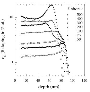
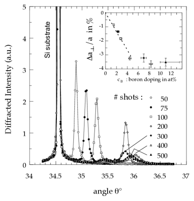
Measurements of boron concentration depth profiles were done by Secondary Ion Mass Spectrometry (SIMS) using a CAMECA IMS4f instrument. Reliable quantification of boron in silicon for such high concentration levels above 1 is a major challenge for SIMS analysis due to matrix effects SIMS as complex ionization and/or sputtering mechanisms may occur during secondary ion emission. We have shown that these effects remain small with an O beam in presence of a saturated oxygen flow at the surface sims O2 . A primary 4keV Osputtering beam of 90nA is rastered at oblique incidence (46.8∘) on 250x250 m2 of the surface. To avoid crater edge effects, 10B+, 11B+, and 29Si+ ions coming from a central part of 10m in diameter have been selected and analyzed simultaneously by an original Isotopic Comparative Method (ICM) (for details see ICM ). Atomic concentrations are presented in Fig. 1 as a function of the depth measured by mechanical profilometry with a Tencor P10. High resolution X-ray diffraction (XRD) curves were then collected around the [004] symmetric Bragg reflection of silicon and are displayed in Fig. 2. A monochromatized excitation source led to an angular resolution better than x degree.
Data shown in Figures 1 and 2 illustrate the significant improvement of the structural quality and sample homogeneity with respect to previous publications Bustarret06 ; GILD . Up to 200 shots (c 4.5 ), we observe relatively flat boron concentrations (Fig. 1) with a sharp interface, at 80 to 90 nm, on the order of 9 nm/decade. The peaks in XRD (Fig. 2) remain very well defined with a full width at half maximum on the order of 0.1∘. As the number of laser shots is increased, the shift to higher diffraction angles illustrates the contraction of the out-of-plane lattice parameter a⟂ as a result of the presence of boron atoms with a smaller covalent radius than silicon. This is a good indication of a sufficiently rapid re-crystallization limiting the diffusion processes and leading to an homogeneous incorporation of boron on substitutional sites far above the solubility limit of 1.2 . In this range, as illustrated by the inset of Fig. 2, the out-of-plane negative strain deduced from the diffraction patterns varied linearly with boron incorporation as measured by SIMS, the slope being in fair agreement with the strain rate coefficient of Vegard’s law in silicon Vailionis99 . Above 200 shots, the interface began to exhibit a shoulder or even a large peak (500 shots) indicating a pileup of boron at the interface during the process. The diffraction peaks did not shift upwards anymore and remained close to 36∘. Their intensity weakened and their width increased substantially, a second weaker broad peak even developing around 35.5∘ for 500 laser shots. This corresponds to a saturation of the out-of-plane strain around -3.5%. Since according to SIMS measurements the intake of boron went on increasing between 200 and 500 shots, one is led to conclude that in this range an increasing fraction of these boron atoms were not incorporated on substitutional sites. In our experience, the saturation value of 36.1∘ observed here for the [004] diffraction peak of Si:B is a quite general upper limit, independent of our GILD operation conditions.
The superconducting temperatures and upper critical field have been deduced from ac-susceptibility () and magneto-transport () measurements. In the measurements, the films have been placed on top of miniature coils and has been obtained by detecting the change in the self induction of the coils induced by the superconducting transitions. Both AC and DC magnetic fields were applied perpendicularly to the doped layer. Approximate corrections were made to account for the demagnetization factor but they don’t affect the determination of where the magnetization is zero. As shown in the inset of Fig. 3, the onset of the diamagnetic response well coincides with the resistive transition, which is remarkably sharp in this sample, 10mK, while being only 5 times larger in the other samples of the series. This allows an accurate determination of and the corresponding values have been reported in Fig. 3 as a function of the B content deduced from SIMS measurements.
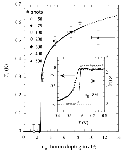
No superconductivity was found down to 40mK for the two less doped samples with c 1.4 (50 laser shots) and c 2.2 (75 laser shots). For higher boron concentration, the critical temperature increases sharply with doping above some critical concentration cc 2.5 reaching 0.6K for cB 8 . For comparison, the sample measured in Bustarret06 displayed a roughly twice smaller with a much broader transition. The apparent saturation of is probably non-intrinsic since the incorporated boron in this range of concentration might be non-electrically active as suggested by XRD and by the observation of a maximum angle of diffraction with broad and less intense peaks (see above). Calculations within Density Functional Theory and Virtual Crystal Approximation Boeri04 predict 0.3K (resp. 3K) for c 5 (resp. 10 ) using MacMillan formula Carbotte . Even if the order of magnitude is correct, the observed dependence of on cB is strikingly different from these predictions. (cB) is actually very similar to that observed in doped diamond, with a critical threshold for doping concentration cc above which increases very sharply with a quasi power law dependence, (. Whereas in doped diamond cc coincides with the critical concentration of the metal-insulator transition, in doped silicon cc 2.5 , i.e. about 300 times larger than the concentration necessary to induce metallicity. The meaning of cc in this latter case remains therefore rather puzzling and needs to be clarified by further studies.
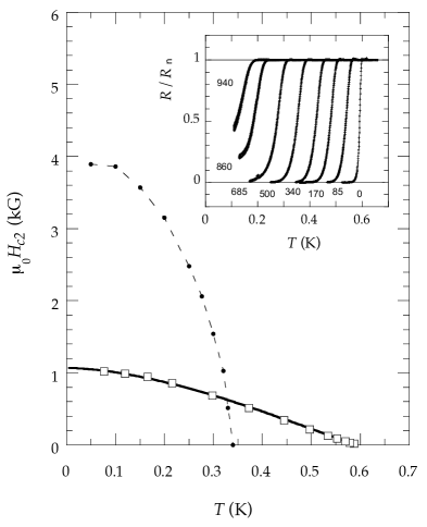
Electrical measurements were performed in magnetic field on the sample with c at.% (400 laser shots) which has the highest and the sharpest transition in zero field. The results are displayed in the inset of Fig. 4 as temperature was swept at different fixed magnetic fields. The transitions was shifted towards lower temperature as the magnetic field was increased, while remaining sharp and well defined. No hysteresis nor supercooling was observed, indicating a second-order transition, which is consistent with doped silicon being a type II superconductor. The upper critical magnetic field , defined by the usual criterion as where the resistance is 90% of its normal state value, is plotted in Fig. 4. Note that the discussion below and the shape of the critical line don’t depend on the exact criterion used; a 50% definition would only shift slightly the line.
The temperature dependence of is very well reproduced within the standard microscopic theory. The full line in Fig. 4 is a fit to the solution of the linearized Gor’kov equations neglecting spin effects HW66 in the very dirty limit, , being the electronic mean-free path and the superconducting coherence length. Both the strong curvature and a 4 times larger (=0K) observed previously Bustarret06 were most probably a consequence of the film inhomogeneity. Since the Fermi velocity is a parameter which cannot be determined experimentally with any accuracy, the electronic mean-free path and were estimated in a simple two-band free electron model Walte04 with light (subscript ) and heavy (subscript ) holes having an effective mass m = 0.16 me (resp. m = 0.49 me), me being the bare electron mass, and with a total carrier concentration of xcm-3. The residual resistivity in this sample was equal to 100cm and . The light hole band is expected to play a minor role for the determination of the upper critical field due to its larger Fermi velocity and its lower partial density of states. In the dirty limit, is therefore related to the electronic mean-free path and to the coherence length in the heavy hole band by: deGennes ; Maki 900 Gauss with being renormalized by the electron-phonon coupling constant, Bustarret06 and with being the superconducting gap. Considering the uncertainties in the thickness of the film and in the geometry of the contacts in a van der Pauw configuration together with the crudeness of a free electron approximation, this estimate Gauss is in good agreement with the experimental data Gauss (see Fig. 4). Note that the London penetration depth = 60nm implying that doped Si should be intrinsically a type I superconductor such as SiC:B Kriener08 but is turned into a type II system by strong impurity effects ( 1 in the dirty limit but 1 in the clean limit).
To conclude, the GILD technique is proved to be a powerful technique to dope silicon in the alloying range where superconductivity occurs. The superconducting transitions are sharp and well defined both in resistivity and magnetic susceptibility allowing the study of the variation of on the boron concentration. This variation is in contradiction with a classical exponential dependence on superconducting parameters. Instead, increases with a quasi-power law form above a critical threshold cc in striking similarity to what is observed in doped diamond. Although in the diamond case cc was equal to the MIT critical concentration, in silicon it lies far above. The comparison of these two cases offers a new playground for studying superconductivity in covalent systems near a MIT.
References
- (1) E. Bustarret, C. Marcenat, P. Achatz, J. Kac̆marc̆ik, et al., Nature (London) 444, 465 (2006).
- (2) J. Nagamatsu, N. Nakagawa, T. Muranaka, Y. Zenitani, and J. Akimitsu, Nature (London) 410, 63 (2001).
- (3) X. Blase, E. Bustarret, T. Klein, C. Chapelier, and C. Marcenat, Nature Materials 8, 375 (2009)
- (4) V.H. Crespi, Nature Materials 2, 650 (2003)
- (5) E.A. Ekimov, V.A. Sidorov, E.D. Bauer, E.D., et al., Nature (London) 428, 542 (2004).
- (6) Z.-A. Ren, J. Kato, T. Muranaka, J. Akimitsu, et al., J. Phys. Soc. Jap. 76, 103710 (2007).
- (7) T. Herrmannsdorfer, V. Heera, O. Ignatchik, M. Uhlarz, et al., Phys. Rev. Lett. 102, 217003 (2009).
- (8) E. Bustarret, J. Kac̆marc̆ik, C. Marcenat, et al., Phys. Rev. Lett. 93, 237005 (2004); T. Klein, P. Achatz, J. Kac̆marc̆ik, et al., Phys. Rev. B 75, 165313 (2007).
- (9) Kerrien et al, Appl. Surf. Sci. 208-209 277 (2003).
- (10) A. Benninghoven, F. Rüdenauer, and H. Werner, Secondary Ion Mass Spectrometry : Basics concepts, Instrumental aspects, Applications and Trends,(WiIey and Sons, New-York, 1987), Chap.3, p. 281
- (11) C. Dubois et al., in Proc. of Int. Conf. on Secondary Ion Mass Spectrometry (SIMS XVII), Toronto, Sept 2009, edited by J. Gardella, to be published
- (12) C. Dubois, G. Prudon, B. Gautier, and J.C. Dupuy, Applied Surface Science 255(4), 1377-1380 (2008).
- (13) A. Vailionis, G. Glass, P. Desjardins, et al, PRL 82, 4464 (1999).
- (14) L. Boeri, J. Kortus, and O. K. Andersen, Phys. Rev. Lett. 93, 237002 (2004).
- (15) J.P. Carbotte, Rev. Mod. Phys. 62, 1027 (1990).
- (16) E. Helfand and N.R. Werthamer, Phys. Rev. 147, 288 (1966).
- (17) A similar analysis was made in the superconductor MgCNi3 in A. Wälte, G. Fuchs, K.-H. Müller, et al., Phys. Rev. B 70, 174503 (2004).
- (18) P.G. de Gennes et al., Phys. Kond. Mat. 3, 79 (1964).
- (19) K. Maki, Physics 1, 21 (1964).
- (20) M. Kriener, Y. Maeno, T. Oguchi, et al., Phys. Rev. B 78, 024517 (2008).