With nonequilibrium Green’s function approach combined with density functional theory, we perform an ab initio calculation to investigate transport properties of graphene nanoribbon junctions self-consistently. Tight-binding approximation is applied to model the zigzag graphene nanoribbon (ZGNR) electrodes, and its validity is confirmed by comparison with GAUSSIAN03 PBC calculation of the same system. The origin of abnormal jump points usually appearing in the transmission spectrum is explained with the detailed tight-binding ZGNR band structure. Transport property of an edge defect ZGNR junction is investigated, and the tunable tunneling current can be sensitively controlled by transverse electric fields.
Polarization Induced Switching Effect in Graphene Nanoribbon Edge-Defect Junction
I INTRODUCTION
With the stunning developments of electronic engineering technology, transistor density of silicon based semiconductor chips is approaching the ultimate size limitation. Innovative materials such as organic moleculesPantelides M ; Reed3 ; Reed2 ; Reed ; Jiang2 ; Liang1 ; Liang2 ; H Chen ; YX Zhou and single-walled carbon nanotubesBaughman (SWNTs) have been suggested as substitutions of conventional semiconductors to implement promising electronic devices in nanoscale where quantum mechanics dominates the electron kinetic behavior.Datta:Electronic Transport in Mesoscopic Systems Graphene, the single layer of carbon honeycomb two-dimensional (D) crystal structure, has become an active field of research because of its exotic physical properties and outstanding electronic quality.A. K. Geim ; Yuanbo Zhang ; K. S. Novoselov ; K. S. Novoselov2 The strong C-C bonds in the plane make graphene an easily available material. Experimental results indicate that, electron mobility of graphene sheet, which is weakly temperature dependent, can be up to cmVs with the carrier density of cm at room temperature.A. K. Geim These exceptional properties make graphene a promising candidate material for nanoscale electronic devices, and have aroused considerable attention in both academic and industrial worlds.IEEE ; Westervelt
Graphene nanoribbons (GNRs) are quasi one-dimensional (1D) structures cut from graphene sheet in particular orientations. They are categorized by the alignment of the edge atoms, namely, zigzag (ZGNR) and armchair (AGNR) ones.Kyoko Nakada With state-of-the-art experimental technology such as direct focused electron writingfocus electron or plasma etchingM. Y. Han , structure modulation of GNR is already possible. Recent first-principles calculation indicates that, in contrast with SWNTs, both ZGNRs and AGNRs are semiconducting, exhibiting band gap increase with the decrease in the ribbon width.Barone ; Young-Woo Son ; Z. Chen ; M. Y. Han Extracting ultra smooth GNRs from solution–derived graphite, Wang and Li et al. composed sub- nm GNR based FETs with considerable on/off ratio due to the semiconducting property of narrow GNRs.Xinran Wang ; Xiaolin Li
To investigate transport properties of nanoscale systems, nonequilibrium Green’s function (NEGF) technique combined with density functional theory (DFT) has been developed into a standard and promising method,Y. Xue ; Datta2 ; J. Taylor ; S. Datta ; Taylor2 which is also widely used in GNR device designing.B DOPING ; Z ; symmetry ; IEEE SYM ; HP Cheng ; FET NEGF ; Different Electrodes ; defect NEGF ; Z2 In this scheme, Liang et al.Different Electrodes compared several graphene based FET contacts, and suggested ZGNRs to be the best choice. With ZGNR source and drain electrodes, Yan et al.Z designed a Z shaped GNR-FET with on/off ratio up to , in which an AGNR is applied in the middle to function as the semiconducting channel. Defects in GNR structures, such as vacancy or doped atoms, are also reported to modify GNR electronic properties significantlyDFCT Structure ; defect NEGF .
In this paper, we apply DFT-NEGF method to simulate GNR based nanoelectronic devices, and a detailed investigation of GNR junctions’ transport properties is carried out. Particular attention is paid to the external electrostatic field controlled switching effects. This paper is organized as follows: In Sec. II, a detailed description of numerical methods and theoretical formulism is presented. Calculated transport properties of GNR devices and the physical origins are given in Sec. III. We summarize our results in Sec. IV.
II THEORETICAL FORMULAS AND CALCULATION DETAILS
In the calculation, the surface Green’s functions of ZGNR electrodes are calculated self-consistently under the DFT based tight binding approximation (TB), while the self-consistent DFT-NEGF transport calculation is applied to the scattering region attached by the left and right electrodes. Both the DFT-TB and DFT-NEGF computations are implemented based on quantum chemistry software GAMESS(US),Gamess1 ; M.S.Gordon while structure optimization and electron structure calculation under periodic boundary conditions (PBC) are carried out by GAUSSIAN03.M.J. Frisch
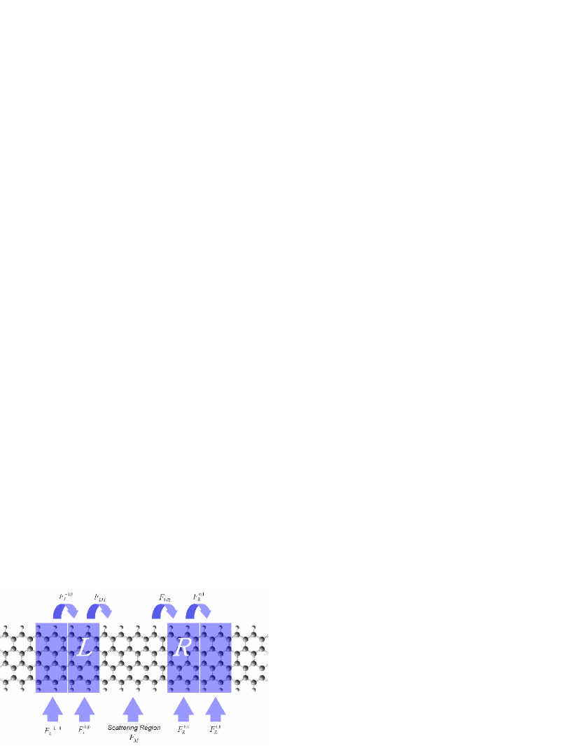
In order to deal with the contact-device-contact open system, semi-infinite ZGNR electrodes and the central scattering region are considered separately. The overall Hamiltonian of the entire open system in Eq.(1) is theoretically an infinite matrix. Atom layers corresponding to the submatrices in Eq.(1) are denoted in Fig.1, where the source and drain electrodes are composed of two semi-infinite ZGNRs with zigzag carbon chains (4-ZGNR). The structure is fully relaxed by DFT geometry optimization under PBC, which is carried out by GAUSSIAN03 under GTO basis 6-31G and B3LYP exchange-correlation term.B3 ; LYP As the starting point of geometry optimization, the C-C and C-H bond lengths of a unit cell are set at Å and Å respectively, and the lattice constant of the perfect quasi-1D crystal is finally relaxed to Å. is the Fock submatrix of the middle scattering region, while and are the submatrices of the contact ”surface” layers of the left and right electrodes respectively. In our NEGF transport simulation, semi-infinite leads are simulated under TB regime, in which only the interactions between the closest TB unit cells are taken into account (). It is lately reported that a TB unit cell of ZGNR should at least include two armchair carbon atom chains to avoid crucial inter-cell interacting information loss.HP Cheng
| (1) |
Combining the electrodes and the scattering region, the open system of GNR junction can be handled as an isolated one with NEGF technique, and the retarded Green’s function of the scattering region is obtained with
| (2) |
where denotes energy plus an infinitesimal imaginary part (), and is the overlap matrix due to the nonorthogonality of the GTO basis set. Including the information of two semi-infinite leads, retarded self energy and are calculated from (), the retarded surface green’s function (SGF) of the interface layer L and R.
| (3) |
(), () are Fock and overlap matrices given by DFT computation of lead-junction-lead open system, describing the interactions between the scattering region and the left (right) electrode. SGFs of contact layers are obtained by transformation matrix method self-consistently with Eq.(4) and Eq.(5) in real space.SGF
| (4) |
| (5) |
Under TB approximation, only the on-site Fock matrix of the left (right) contact layer () and the closest neighbor interaction () are involved in the SGF self-consist calculation. With retarded Green’s function of the scattering region, the density matrix can be given as
| (6) |
where is the advanced Green’s function of the scattering region. denotes the electrode-device coupling matrix; = represents Fermi distribution of the left and right lead respectively, in which is the environment temperature of the junction, is the chemical potential for source and drain, and stands for Fermi level of the semi-infinite leads.
Because of charging effect and level broadening in the scattering region caused by electrode-device coupling, density matrix , Fock matrix , and retarded Green’s function must be calculated self-consistently. First, the converged density matrix of isolated cluster based DFT calculation is applied as the initial guess. Then, we use the open system self-consistent iteration loop to replace the original cluster-based DFT loop of GAMESS(US) to obtain the density matrix from Eq.(6). The loop will not be stopped until the updated density matrix meets the convergence criteria.
With converged , the total tunneling current of the open system at certain temperature can be given by Landauer-Bütiker equationR. Landauer
| (7) |
| (8) |
where is the transmission function.
From the NEGF approach, the infinite open system can be solved as an isolated one. In this work, DFT-NEGF computation is performed under real-space GTO with the smallest effective core potential CEP-4G.CEP-4G Becke-3 hybrid functional and Perdew-Wang-91 gradient-corrected correlation functionalB3 ; PW91 are used as the exchange-correlation part.
To guarantee the validity of the TB approximation for Eq.(4) and Eq.(5), we compare the TB band structure for the perfect 4-ZGNR with a periodical boundary condition (PBC) result in GAUSSIAN03, where all inter-cell couplings are included.
Since GTO basis functions are originally denoted in real space, to calculate the band structure of an infinite 1D bulk crystal, one need to transform the Fock and overlap matrices to reciprocal space,
| (9) |
where denotes the DFT Fock operator of a unit cell of the quasi-1D crystal, and is its matrix element in Bloch wave representation with standing for the coupling Fock matrix element between lattice and in real-space. Theoretically, the summation in Eq.(9) goes over all lattices in real-space (). However, under TB approximation, the summation in Eq.(9) has only three terms considered, including the on-site Hamiltonian and the nearest neighbor coupling Hamiltonian .
| (10) |
And is calculated likewise
| (11) |
Applying GAMESS(US) combined with NEGF subroutines, we first carry out the DFT-NEGF calculation of the 4-ZGNR junction (Fig.1) under zero source-drain bias. Then, real-space matrices , , , and are extracted from the converged result. Substituting , , , and in Eq.(10, 11) with the extracted matrices respectively, TB band structure of quasi-1D 4-ZGNR can be obtained by solving Roothaan equation
| (12) |
We obtained a spin-polarized zero temperature ground state on 4-ZGNR with spin dependent DFT-LSDA calculation, where the energy of the spin-polarized state is about 20 meV per edge atom lower than the spin-unpolarized one, similar to the results obtained by Son et al.Young-Woo Son However, the magnetic order of ZGNR is reported to be unstable in the presence of ballistic tunneling current under room temperature.Denis A. Areshkin ; symmetry ; D.Gunlycke ; H.Wagner ; Z Thus, we present a ZGNR device simulation under room temperature with spin-unpolarized calculation in this work.
III RESULTS AND DISCUSSIONS
First, we apply NEGF-DFT calculation to the optimized structure of the perfect quazi-1D 4-ZGNR, where two central unit cells including 32 carbon atoms are treated as the scattering region between the contact layers and periodic ZGNR electrodes (Fig.1). PBC calculation of the system is also performed by GAUSSIAN03 with exactly the same basis functions and DFT calculation setup (CEP-4G and B3PW91) to check the validity of our TB approximation.
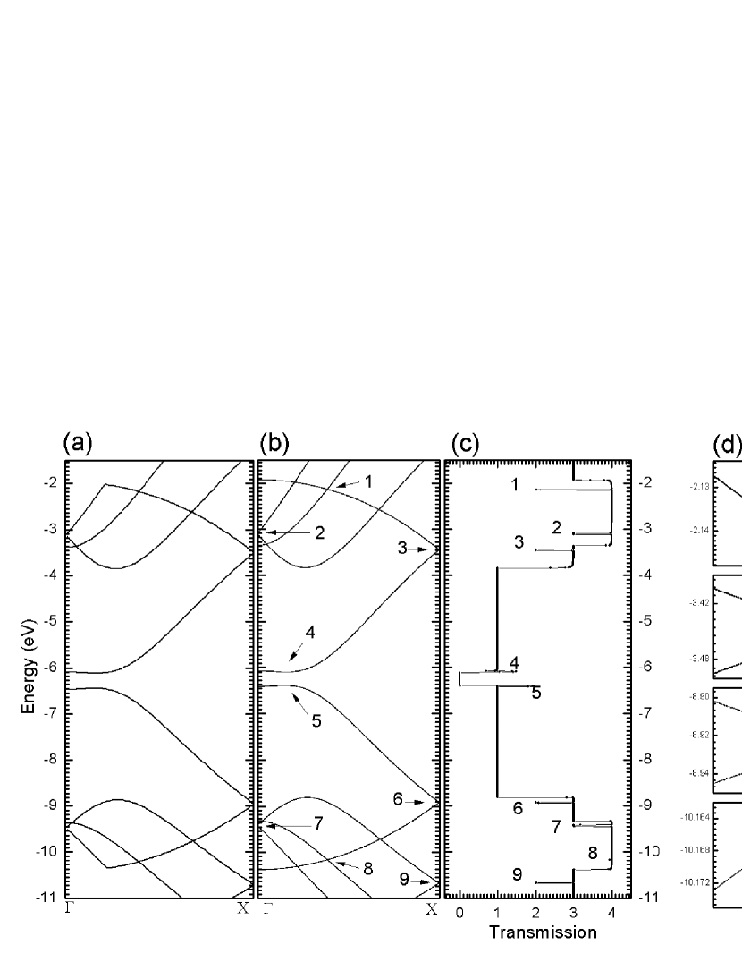
In Fig.2(a), the 4-ZGNR’s PBC band structure provided by GAUSSIAN03 exhibits its semiconductor properties with a band gap of eV, while the DFT-based TB band structure for the same system is presented in Fig.2(b) for comparison. Here, ( eV) is at the center of the band gap of 4-ZGNR. The result plotted is a so called ”folded version” because the unit cell is enlarged to include two armchair carbon layers. Comparing Fig.2(a) and (b), the DFT-based TB band structure (b) corresponds with the PBC result (a) perfectly, indicating that although only and are included in the calculation, TB approximation can still accurately predict the bulk property of 4-ZGNR: almost all the interactions out of TB range are neglectable.
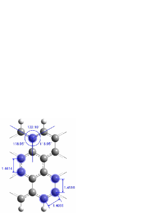
The semiconducting property of 4-ZGNR originates from two factors. In addition to the transverse quantum confinement of the extremely narrow 4-ZGNR (about nm wide), the broken perfect honeycomb structure near the GNR edges opens the gap on the band structure. As presented in Fig.3, the edged C-C bond lengths of 4-ZGNR are no longer identical to the ones in the perfect honeycomb structure, and the bond angles deviate from after structure relaxation. The reconfiguration of structure breaks the perfect hexagon symmetry, which generates the band gap between and * states. The semiconducting property of 4-ZGNR has its disadvantage because of the poor conductance under low bias. However, the C-C bonds between the leads and the scattering region are very strong, which avoids the uncontrollable contact diversity on the interface between organic molecules and metal leads. Our further calculation indicates that, with the increase in the width of ZGNR, the gap gradually vanishes, and the unworking region of ZGNR will be reduced. The width of GNR realized in experiments are rarely smaller than nm nowadays, which is much wider than the 4-ZGNR considered in this work, making ZGNRs suitable to be applied as lead material in realistic nanoscale circuits. However, the NEGF-DFT simulation of a nm ZGNR is extremely time consuming and requires enormous computational resources. In this work, we are not trying to reproduce an actual experimental situation, but to demonstrate theoretically the relationship between the band structure and the transmission spectrum for a simple 4-ZGNR system, and to propose the mechanism that might control the transport behavior of ZGNR devices.
The transmission spectrum calculated under zero bias is shown in Fig.2(c) with several integer steps and narrow jump points, which is consistent with the band structures made by our DFT-based TB (b) or g03 PBC (a) calculations. This is the usual characteristics of the transmission spectrum for infinite lead. Similar appearances were reported by other works for the study of quazi-1D systems.HP Cheng ; symmetry ; XG Zhang
In such a perfect 1D crystal without any defects, each Bloch state can tunnel through the junction without any classical resistance, and contribute a unit of quantum conductance for the total transmission spectrum. The integer steps in the transmission spectrum indicate the number of the conducting channels or Bloch states. For the electrons with energy closely higher than eV, where cross three curves, three Bloch states function as conducting channels, so the transmission spectrum is around this energy value. In another case, the band structure crosses the energy of eV four times, so that the transmission here is . In this regime, for any energy value under consideration, one can accurately predict the transmission coefficient for the perfect quasi-D crystal simply by counting the number of Bloch state in the electronic structure. The narrow ”jump points” in transmission spectrum (Fig.2(c)) are labeled from to . They are not caused by numerical inaccuracy, but induced by the sudden change in the number of the conduction channels. In Fig.2(d) we enlarge the band structure around the points to show that there are mini-gaps rather than band crossings corresponding to the transmission abnormal points. Investigating carefully, one may find that the number of Bloch states changes from one to two then zero when the relevant energy scan up across the maximum of the band then entering the mini-gap (point ), which causes the transmission value varied from one to two then zero. The sudden vanishment of two Bloch states inside the narrow band gap of eV explains the sharp drop of two quantum conductance units in the transmission function at point . The jump points , , , and are all companied by the small band gaps on or X points, generating a decline of one quantum conductance unit in the transmission function at the relevant energy values due to the absence of one Bloch state. Interestingly, the runtish point fails to achieve an integer drop. Its exotic behavior is caused by the tiny mini-gap of eV, which is very hard to demonstrate by the transmission function with the numerical sampling step length as large as eV. Fortunately, tunneling current is evaluated by the integral of transmission spectrum, and the numerical error like point does not influence the result significantly even if the error is included in the bias window. It should be pointed out that although not shown here, all other crossings in the TB band structure are also investigated in details, with sampling k points from to X. No band gaps can be observed at the energy values where no abnormality exists on transmission function, demonstrating a very accurate matching between DFT-NEGF calculated transmission and the DFT-TB band structure. This matching assures the validity of the SGF of left (right) electrode, which is obtained by the DFT-TB calculation.
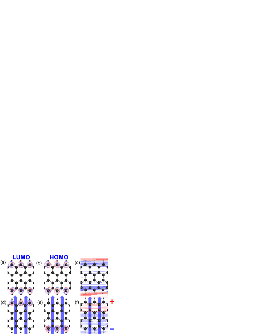
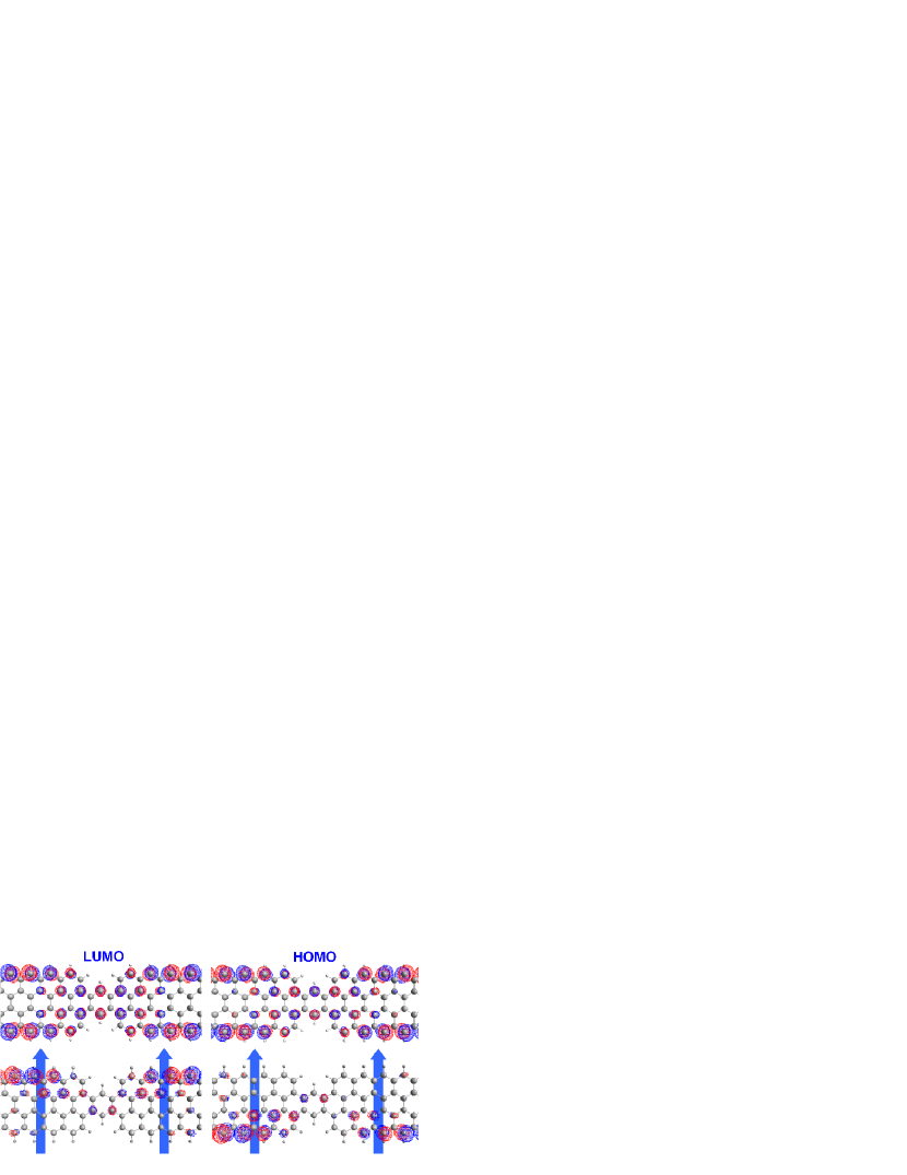
In order to investigate the external electrostatic field response in 4-ZGNR, homogeneous transverse electric fields are applied to the scattering region. The orientation of external field is arranged perpendicularly to the GNR axis (shown in Fig.4), with the intensity of V/Å ( a.u.). By the help of MacMolPlt,Bode 3D HOMO LUMO and 2D molecular electrostatic potential (MEP) distribution of pure 4-ZGNR are presented in Fig.4 with the 2D plotting major plane parallel to the ZGNR and Å away from it. The flat surface of 2D MEP map is specifically chosen to reveal the electrostatic potential contributed by the and hybridized orbitals, which are mainly formed by the overlap of orbital of carbon atoms. The red contours are positive potential isolines, while the blue ones are negtive. We note that the MEP plot is generated based on the optimized orbitals and occupations computed by GAMESS in the presence of the external field, subttracting the contribution of the external field itself. Similar to previous works, HOMO and LUMO are equally distributed on edges, and the magnitude of electron wave function decays from edge to the center gradually.Young-Woo Son Under external fields, the molecular orbitals of and are splitted as the consequence of electric polarization: HOMO concentrated at the low-potential edge, while LUMO at the high-potental edge. Unfortunately, the transmission function of pure ZGNR (not shown here) hardly responds to external fields: the fields can only control the orbital coupling in the direction perpendicular to the tunneling current.
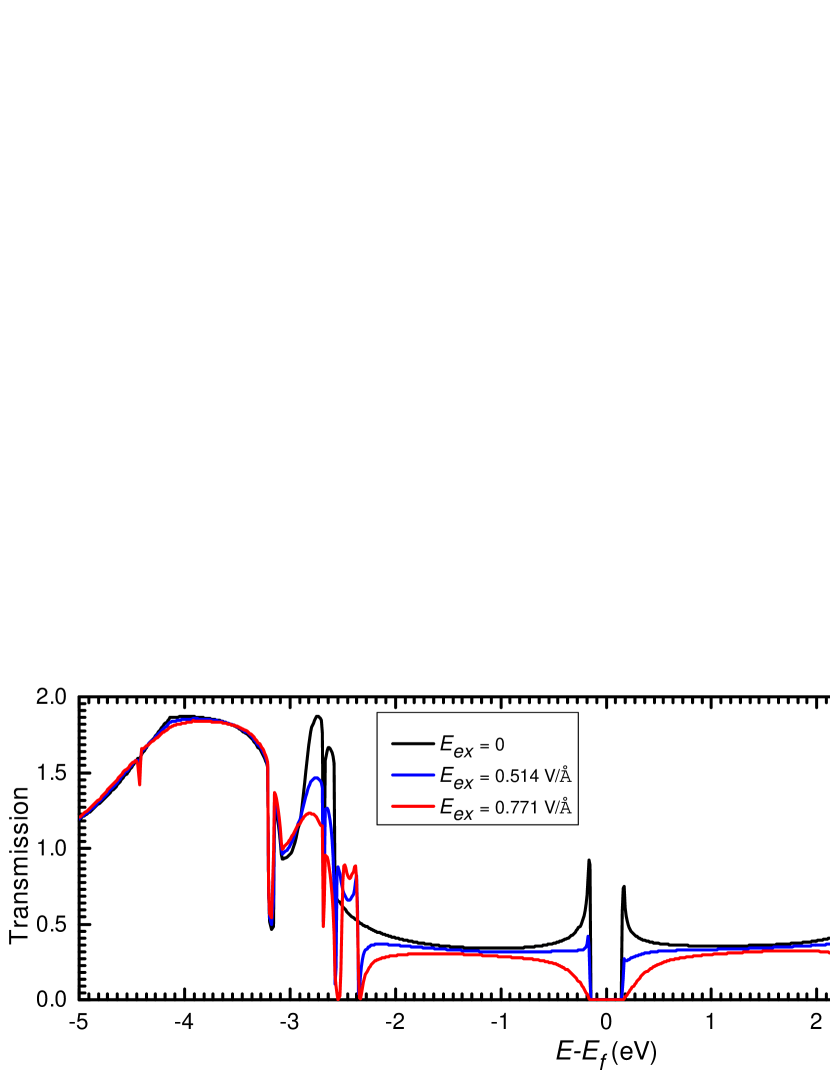
In recent first-principle calculations, some groups indicate that vacancies on GNR edges are energetically preferredDFCT Structure , which significantly suppresses GNRs’ conductance.defect NEGF Here, we fabricate GNR edge defects by removing three carbon atoms from the edges of 4-ZGNR, with the dangling bonds saturated by hydrogen atoms. The central junction structure including 58 carbon atoms is optimized with the left and right leads fixed in their PBC optimized positions. The contact layers are kept out of the TB range from the central defect region, so that their ”bulk” properties are protected by the buffer layers. Optimization result indicates that, all carbon and hydrogen atoms in the defect region are still in the same plane after relaxation, and the saturating hydrogen atoms pushes the edge carbon atoms off the vacancy significantly. The equilibrium transmission spectrum of the edge defect junction is presented in Fig.5 with the external field adjusted from to V/Å ( a.u.). Polarization effect stimulated by the transverse external fields for the HOMO and LUMO distribution is shown in Fig.6 respectively. Similar to reported results, the GNR defect junction exhibits about 50% decline of transmission around under zero external fields. This drastic conductance depression is obvious because pure ZGNR’s HOMO and LUMO are mainly distributed on edges so that their orbital coupling in the tunneling direction is significantly suppressed with edge defects presented. As plotted in Fig.6, edge vacancies break two of the six-sided carbon rings, and the C-C sp2 hybridization of and MO is substituted by the localized C-H bonds on the edge vacancy, leading to a radical disruption of the delocalized conjugated system.
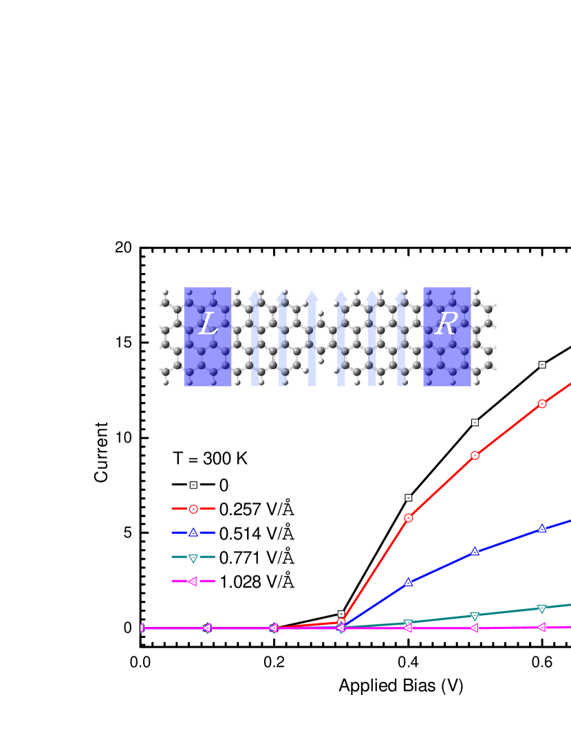
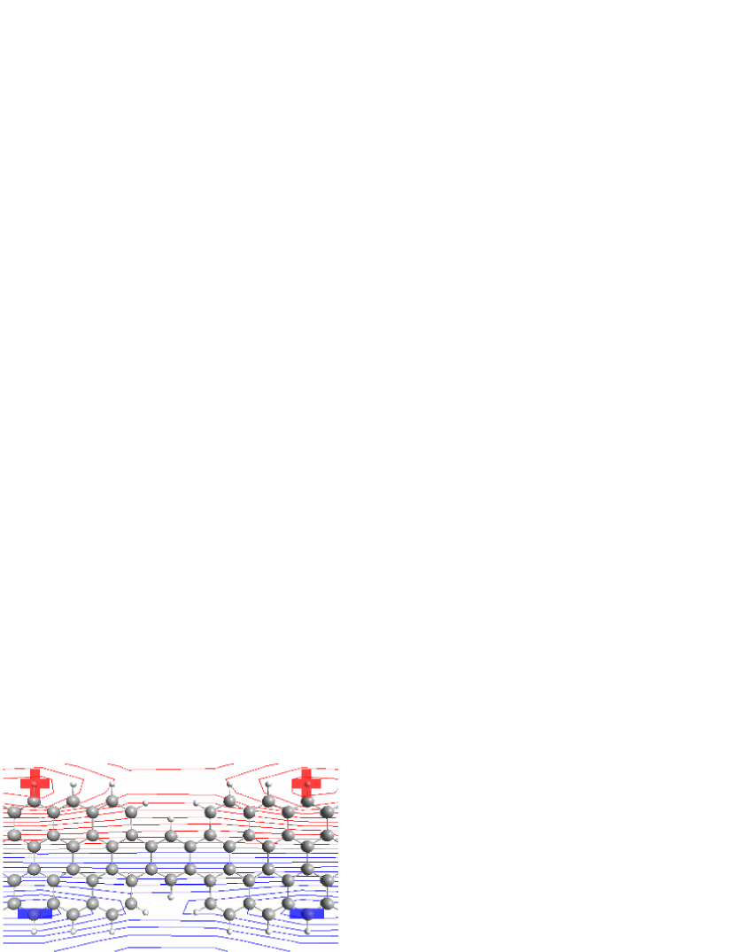
Although the conductance of defect junction is no better than pure ZGNR, the presence of edge defects makes it more sensitive to the modulation of external transverse electric fields, which leads the possible application of the defect ZGNR junctions to nanoscale electronic engineering. The I-V curve of the defect junction given by Eq.(7) is presented in Fig.7, in which a very clear depression of tunneling current can be observed under large transverse external fields. In this calculation, the temperature of Fermi distribution is set at room temperature (K). The low conductance under the voltage V is caused by the HOMO-LUMO gap of 4-ZGNR. The tunneling current increases considerably with applied bias exceeding the gap threshold. In the presence of external fields, the junction almost turns off the conducting channel when exceeds V/Å, exhibiting the maximum of the on/off ratio up to . Similar with the situation of pure ZGNR, LUMO and HOMO of the defect junction are no longer symmetrically distributed when is applied. HOMO (electron states) and LUMO (hole states) are polarized to opposite edges.(Fig.6) Contrasting to pure 4-ZGNR, electric polarization depresses the local orbital coupling of the central region to the GNR electrode much more severely as a consequence of the edge vacancies, producing significant difficulties for electrons to tunnel through the junction. To present a clearer mechanism of the conductance decay induced by electric polarization, MEP map of the junction’s scattering region is plotted in Fig.8 with the potential of external field subtracted off. The isoline circles in the MEP indicate charge concentration induced by polarization, with positive charge conglomerated on the upper edge, and the negative one on the opposite. Functioning together with the geometry shape, tunable external fields splits the electron wave function with a potential barrier constructed on the edge vacancies, reflecting the carriers back to the electrodes. Since no structural modification is required in the control process, conductance manipulation based on electric polarization is more sensitive to external stimulus, so GNR edge defect junctions have the potential to be applied as switching devices with considerable responding frequencies under the control of transverse electric fields. On the other hand, for a pure 4-ZGNR without any vacancy, although polarization exits, the potential barrier can not be established, hence the tunneling current barely responds to sensitively.
IV SUMMARY
In summary, we use DFT-NEGF method to simulate the transport properties of 4-ZGNR, and find out that edge defects make the tunneling current of ZGNR junctions more controllable by the transverse external electrostatic fields. In this work, ZGNR electrodes are modeled with DFT-based TB approximation, and the validity of the approximation is assured by comparison between the perfect ZGNR band structures calculated under our DFT-based TB and GAUSSIAN03 PBC calculations. Using DFT-based TB method, we obtain the transmission function of the perfect ZGNR system, of which the integer steps and jump points are explained well by the band structure. Electronic devices made from the edge defect ZGNR junctions have the advantage of easy control through the transverse electrostatic fields. The study of small and narrow GNR devices benefits graphene integrated circuit engineering that might be realized by ultra fine GNR fabrication technologies in the future.
Acknowledgements.
We feel grateful for constructive and inspiring discussions between one of us (G.Y.) and Prof. Xiao-Guang Zhang at ORNL. This work is also sponsored by Natural Science Foundation of China (NSFC) under Grant No. 90606024, the Program for Major Research Plan of China (Project No. 2006CB 921302), and Nippon TechnoLab Co. Ltd. We thank the support from Fudan High-end Computing Center, Shanghai Supercomputer Center, and SR11000 supercomputer from the Center for Computational Materials Science of Institute for Materials Research, Tohoku University.References
- (1) M. A. Reed, and J. M. Tour, Sci. Am. 282, 86, (2000).
- (2) M. A. Reed, C. Zhou, C. J. Muller, T. P. Burgin, and J. M. Tour, Science 278, 252 (1997).
- (3) J. Chen, M. A. Reed, A. M. Rawlett, and J. M. Tour, Science 286, 1550 (1999).
- (4) M. Di Ventra, S. T. Pantelides, and N. D. Lang, Phys. Rev. Lett. 84, 979 (2000).
- (5) F. Jiang, Y. X. Zhou, H. Chen, R. Note, H. Mizuseki, and Y. Kawazoe, Phys. Lett. A 359, 487, (2006).
- (6) Y. Y. Liang, F. Jiang, Y. X. Zhou, H. Chen, R. Note, H. Mizuseki, and Y. Kawazoe, J. Chem. Phys. 127, 084107 (2007)
- (7) Y. Y. Liang, Y. X. Zhou, H. Chen, R. Note, H. Mizuseki, and Y. Kawazoe, J. Chem. Phys. 129, 024901 (2008).
- (8) Y. X. Zhou, F. Jiang, and H. Chen, R. Note, H. Mizuseki, and Y. Kawazoe, J. Chem. Phys. 128, 044704 (2008).
- (9) H. Chen, J. Q. Lu, J. Wu, R. Note, H. Mizuseki, and Y. Kawazoe, Phys. Rev. B 67, 113408 (2003).
- (10) R. H. Baughman, A. A. Zakhidov, and W. A. de Heer, Science 297, 787 (2002).
- (11) S. Datta, Quantum Transport: Atom to Transistor, (Cambridge University Press, Cambridge, 2005).
- (12) A. K. Geim and K. S. Novoselov, Nature Materials 6, 183 (2007).
- (13) K. S. Novoselov, A. K. Geim, S. V. Morozov, D. Jiang, M. I. Katsnelson, I. V. Grigorieva, S. V. Dubonos, and A. A. Firsov, Nature (London) 438, 197 (2005).
- (14) K. S. Novoselov, A. K. Geim, S. V. Morozov, D. Jiang, Y. Zhang, S. V. Dubonos, I. V. Grigorieva, A. A. Firsov, Science 306, 666 (2004).
- (15) Y. Zhang, Y. W. Tan, H. L. Stormer, and P. Kim, Nature (London) 438, 201 (2005).
- (16) M. C. Lemme, T. J. Echtermeyer, M. Baus, and H. Kurz, IEEE Electron Dev. Lett. 28, 282 (2007).
- (17) R. M. Westervelt, Science 320, 324 (2008).
- (18) M. Remeika and A. Bezryadin, Nanotech. 16, 1172 (2005).
- (19) K. Nakada, M. Fujita, G. Dresselhaus and M. S. Dresselhaus, Phys. Rev. B 54, 17954 (1996).
- (20) Y. Son, M. L. Cohen, and S. G. Louie, Phys. Rev. Lett. 97, 216803 (2006).
- (21) V. Barone, O. Hod, and G. E. Scuseria, Nano Letters 6, 2748 (2006).
- (22) Z. Chen, Y-M Lin, M. J. Rooks and P. Avouris Physica E 40, 228 (2007).
- (23) M. Y. Han, B. .zyilmaz, Y. Zhang, and P. Kim, Phys. Rev. Lett 98, 206805 (2007).
- (24) Denis A. Areshkin and Carter T. White, Nano Lett. 7, 3253 (2007).
- (25) Daniel Gunlycke, Denis A. Areshkin, Junwen Li, John W. Mintmire, and Carter T. White, Nano Lett. 7, 3608 (2007).
- (26) N. D. Mermin and H. Wagner, Phys. Rev. Lett. 17, 1133 (1966).
- (27) X. Wang, Y .Ouyang, X. Li, H. Wang, J. Guo, and H. Dai, Phys. Rev. Lett. 100, 206803 (2008).
- (28) X. Li, X. Wang, L. Zhang, S. Lee, H. Dai, Science 319, 1229 (2008).
- (29) Y. Xue, S. Datta, M. A. Ratner, Chem. Phys. 281, 151 (2002).
- (30) S. Datta, Superlattices Microstruct. 28, 253 (2000).
- (31) Y. Xue and M. A. Ratner, Phys. Rev. B 68, 115406 (2003).
- (32) J. Taylor, H. Guo, and J. Wang, Phys. Rev. B 63, 245407 (2001).
- (33) M. Brandbyge, J. Mozos, P. Ordejón, J. Taylor, and K. Stokbro, Phys. Rev. B 65, 165401 (2002).
- (34) L. A. Agapito and H. P. Cheng, J. Phys. Chem. C 111, 14266 (2007).
- (35) G. Fiori and G. Iannaccone, IEEE Electron Dev. Lett. 28, 760 (2007).
- (36) T. B. Martins, R. H. Miwa, Antônio J. R. da Silva, and A. Fazzio, Phys. Rev. Lett. 98, 196803 (2007).
- (37) G. Liang, N. Neophytou, M. S. Lundstrom, and D. E. Nikonov, Nano Lett. 8, 1819 (2008).
- (38) G. Liang, N. Neophytou, and M. S. Lundstrom, D. E. Nikonov, J. Appl. Phys, 102, 054307 (2007).
- (39) N. Gorjizadeh, A. A. Farajian and Y. Kawazoe, Nanotech. 20, 015201 (2009).
- (40) Q. Yan, B. Huang, J. Yu, F. Zheng, J. Zang, J. Wu, B. Gu, F. Liu, and W. Duan, Nano Lett. 7, 1469 (2007).
- (41) Z. F. Wang, Q. Li, Q. W. Shi, X. P. Wang, J. G. Hou, H. X. Zheng, and J. Chen, Appl. Phys. Lett. 92, 133119 (2008).
- (42) Z. Li, H. Qian, J. Wu, B. Gu, and W. Duan, Phys. Rev. Lett. 100, 206802 (2008).
- (43) M. Topsakal, E. Aktürk, H. Sevinçli, and S. Ciraci, Phys. Rev. B 78, 235435 (2008).
- (44) M. W. Schmidt, K. K. Baldridge, J. A. Boatz, S. T. Elbert, M. S. Gordon, J. H. Jensen, S. Koseki, N. Matsunaga, K. A. Nguyen, S. J. Su, T. L. Windus, M. Dupuis, J. A. Montgomery, J. Comput. Chem. 14, 1347 (1993).
- (45) M. S. Gordon and M. W. Schmidt, Theory and Applications of Computational Chemistry: the first forty years, edited by C. E. Dykstra, G. Frenking, K. S. Kim, and G. E. Scuseria, (Elsevier, Amsterdam, 2005), pp. 1167-1189.
- (46) M. J. Frisch, G. W. Trucks, H. Schlegel et al., GAUSSIAN 03, Revision D. 01, Gaussian, Inc., Wallingford CT, 2004.
- (47) A. D. Becke, Phys. Rev. A 38, 3098 (1988).
- (48) C. Lee, W. Yang and R. G. Parr, Phys. Rev. B 37, 785 (1988).
- (49) W. J. Stevens, H. Basch, and M. Krauss, J. Chem. Phys. 81, 6026 (1984).
- (50) J. P. Perdew and Y. Wang, Phys. Rev. B 45, 13244 (1992).
- (51) E. J. Mele and J. D. Joannopoulos, Phys. Rev. B 17 1816 (1978).
- (52) R. Landauer, IBM J. Res. Dev. 1, 233 (1957).
- (53) Y. Son, M. L. Cohen, and S. G. Louie, Nature (London) 444, 347 (2006).
- (54) P. S. Krstic, X. G. Zhang, and W. H. Butler, Phys. Rev. B 66, 205319 (2002).
- (55) B. M. Bode and M. S. Gordon, J. Mol. Graphics and Modeling 16, 133 (1998).
Captions
-
FIG. 1. (Color online) The arrangement of 4-ZGNR based junction after geometry optimization with dangling bonds on zigzag edges saturated by hydrogen atoms. Two armchair carbon layers are included in each TB unit cell to avoid sever inter-cell interaction loss of TB approximation. In DFT-NEGF calculation for a pure 4-ZGNR, two TB unit cells are treated as the scattering region between the left and right contact layers.
-
FIG. 2. Band structure of perfect 4-ZGNR quasi-D crystal drawn under (a) periodic boundary condition and (b) tight-binding approximation. Only 8 energy bands around the Fermi level are presented in the PBC band structure. Transmission spectrum of the scattering region (c) is presented with 9 narrow transmission jump points. Detailed band structures around these points are demonstrated in (d).
-
FIG. 3. (Color online) Fully relaxed unit cell alignment of 4-ZGNR: the perfect graphene honeycomb structure is broken, which is one of the reasons of 4-ZGNR’s semiconducting property. Length unit in this plot is Å.
-
FIG. 4. LUMO (a)(d) and HOMO (b)(e) distribution on pure 4-ZGNR. Positive (red) and negative (blue) 2D molecular electrostatic potential (MEP) isolines of pure ribbon are shown in (c) and (f). The arrows in (d), (e), and (f) indicate the transverse external field.
-
FIG. 5. Zero bias transmission spectrum of edge defect junction.
-
FIG. 6. LUMO and HOMO of edge defect junction, with indicated by blue arrows.
-
FIG. 7. I-V curves of edge defect junction in modulation of the intensity of transverse electric field. The inset shows the optimized structure of edge defect junction and the setup of the scattering region. The environment temperature of this simulation is K.
-
FIG. 8. 2D electrostatic potential distribution of edge defect junction. The plotting plane is parallel to the ribbon, and 1.2 Å away from it.